
A comprehensive study on the effects of gamma radiation on the physical properties of a two-dimensional WS2 monolayer semiconductor†
Jorlandio Francisco
Felix
 *a,
Arlon Fernandes
da Silva
a,
Sebastião Willam
da Silva
a,
Fanyao
Qu
a,
Bin
Qiu
b,
Junfeng
Ren
b,
Walter Mendes
de Azevedo
c,
Mohamed
Henini
d and
Chung-Che
Huang
*e
*a,
Arlon Fernandes
da Silva
a,
Sebastião Willam
da Silva
a,
Fanyao
Qu
a,
Bin
Qiu
b,
Junfeng
Ren
b,
Walter Mendes
de Azevedo
c,
Mohamed
Henini
d and
Chung-Che
Huang
*e
aInstitute of Physics, Nucleus of Applied Physics, University of Brasília, Brasília-DF 70919-970, Brazil. E-mail: Jorlandio@unb.br
bSchool of Physics and Electronics, Shandong Normal University, Jinan, 250014, China
cDepartamento de Química Fundamental, Universidade Federal de Pernambuco, Recife, 50670-901, Brazil
dSchool of Physics and Astronomy, University of Nottingham, Nottingham NG7 2RD, UK
eOptoelectronics Research Centre, University of Southampton, Southampton, SO17 1BJ, UK. E-mail: cch@orc.soton.ac.uk
First published on 2nd October 2019
Abstract
This article reports the effects of gamma radiation on the structural, optical and magnetic properties of monolayer tungsten disulfide (WS2) grown by a scalable van der Waals epitaxial (VdWE) process on a SiO2 coated Si substrate. We found that ionizing radiation (gamma ray) interacts strongly with two-dimensional WS2, which induces effective p-doping in the samples. As the radiation dose increases, the p-doping concentration increases substantially. In addition, in the small radiation dose regime, the WS2 monolayers exhibit usual diamagnetic behavior. However, a remarkable ferromagnetic hysteresis emerges when the WS2 monolayer is irradiated with 400 Gys. This is attributed to the presence of irradiation-induced complex vacancies composed of one tungsten and a pair of its nearby sulfurs. Moreover, these results have shown that the detector based on the large scale monolayer VdWE-grown two-dimensional WS2 is an appealing candidate for sensing high-energy photons at small radiation doses.
New conceptsWe report, for the first time, the effects of gamma radiation on the structural, optical and magnetic properties of monolayer WS2 grown by a scalable van der Waals epitaxial (VdWE) process on SiO2/Si substrates. We demonstrated experimentally that gamma irradiation dramatically affects the physical properties of monolayer WS2. For example, when the γ-irradiation dose increases, a blue Raman shift of the A1g(Γ) peak, an increase of the Raman intensity ratio between A1g(Γ) and E12g(Γ) modes and an enhancement of the trion emission intensity have been observed. This indicated that the irradiation creates vacancies and induces effective p-doping. More interestingly, a transition from diamagnetic to ferromagnetic phase emerges when a WS2 monolayer is irradiated with 400 Gys intensity. Our first principles calculations illustrate that the magnetism originates from the complex vacancies composed of one tungsten and a pair of its nearby sulfurs. In addition, we also shown that the detector based on the monolayer WS2 possesses a high sensitivity for detection of low doses of gamma ray radiation. Our work is novel, timely and presents interesting results concerning the effects of γ-irradiation on the physical properties of monolayer TMDC materials. Our findings are relevant for room temperature gamma radiation detectors and space instrumentations. |
Introduction
Since the emergence of graphene as the first free-standing two-dimensional (2D) material, the class of layered 2D materials has expanded quickly. It spans a great diversity of atomic structures and physical properties.1–14 Amongst them prominent 2D materials are transition metal dichalcogenides (2D-TMDCs).1,2 A notable feature of the TMDCs is a transition from an indirect band gap to a direct band gap when thinned from bulk to a monolayer, which significantly enhances the photoluminescence (PL) intensity.1 Furthermore, tunable electronic properties, structural controllability, and unique spin valley-coupled properties such as valley selective circular dichroism make the TMDCs a promising platform for exploring new optoelectronic and valleytronics device applications such as photovoltaic light sensors,2 photonics,3 flexible nanoelectronics,4 energy storage,5,6 integration with silicon technology, low-loss nanophotonics,12 and high on/off output current ratio FETs.13 In addition, the devices based on 2D TMDCs are characterized by small size, light weight and low power consumption. This makes them advantageous for use in space instrumentation.Inversion symmetry and strong spin–orbit interaction endow WS2 with especially well-defined spin-splittings around the K- and K′ valley, which is very desirable for spintronics applications. If a nonmagnetic WS2 monolayer could be endowed with robust room-temperature ferromagnetism, it could be expected that it will not only act as an ideal spintronics channel material for nanodevices but also provide an excellent platform for studying the relationship between electronic and magnetic properties of quantum-confined structure matters. Hence incorporating a magnetic moment into 2D materials will open up novel opportunities to study new physics and many appealing potential applications.
The performance of devices is usually affected by their surrounding environment, e.g., radiation, air, etc. For 2D materials, these effects become even prominent due to their high surface/volume ratio and ultrathin thickness. Therefore, revealing and having a good understanding of the effects of radiation on the physical properties of 2D TMDCs are crucial either during or prior to their device applications.4,15–17 For instance, the space environment contains different levels of radiation,18,19 which might induce variations of the physical properties of constituting 2D-TMDCs used for long-term mission satellites and/or spacecraft for space exploration. Consequently, it might cause some disturbances to these devices, therefore affecting the normal operations of the electronics. Therefore, knowledge of the effect of ionizing radiation on 2D-TMCs becomes a key issue for determining whether or not they are suitable for space-based applications, where device miniaturization is highly required for weight reduction and compactness.20 Recently, extensive investigations have been performed and many interesting novel phenomena have been discovered.21 For instance, Iqbal et al.8 studied the effect of deep-ultraviolet (DUV) light in nitrogen (N2) and oxygen (O2) gas atmospheres on device performance of exfoliated single-, bi-, and multi-layered WS2 FETs. They have shown an n-type doping effect after DUV irradiation, and WS2-based FETs showed an enhanced charge carrier density, mobility and photocurrent response.8 In an experimental investigation, the structural damage or degradation of a 2D WS2 crystal was observed by Atkin et al., when it was exposed to a laser beam in the presence of ambient moisture.15 Ma et al. demonstrated that Ar+ ion irradiation creates S-vacancies in the WS2 monolayer, resulting in an enhancement of the saturable absorption in the NIR region.16 Using oxygen irradiation, Song et al. showed that it is possible to modify the multilayer WS2 nanosheets with precisely tailored layer-structures and controllable optical band gap.17 In addition to these experimental observations, Yoshimura et al.14 theoretically studied the effect of electron beam irradiation on 2D-TMDCs, using density functional theory (DFT) together with relativistic scattering theory. They report the possibility of creating complex defects, but without significant damage to the TMDC crystal. Although extensive investigations about radiation effects, using different radiation types, have been carried out, no study investigated the influence of γ-ray radiation on the optical and magnetic characteristics of 2D materials, especially for monolayers of TMDCs such as monolayer WS2. Moreover, due to technical challenges, no irradiation-induced room temperature ferromagnetic ordering in TMDC monolayers has been detected yet.
In this work, the effects of 60Co gamma radiation dose on the structural, optical and magnetic properties of WS2 monolayers are examined and discussed. X-ray photoelectron spectroscopy (XPS) results demonstrate that the radiation creates defects and their density increases with the radiation dose. PL and Raman spectroscopy measurements provide further support to XPS results. Interestingly, the conversion from diamagnetic to ferromagnetic phase in monolayer WS2 irradiated by gamma rays has been detected at room temperature. The origin of the ferromagnetism has been identified with the help of ab initio calculations.
Results and discussion
The effect of γ-radiation on the structural properties of 2D-WS2 has been investigated by Raman spectroscopy, which is a widely used tool to characterize the defects in 2D materials.8,22,23Fig. 1 shows room temperature Raman spectra using 514.5 nm excitation of the non-irradiated (NI) and irradiated samples. The former serves as a reference and the latter is the sample irradiated with 1000 Gys. As shown in Fig. 1 both samples exhibit typical Raman signatures of monolayer WS2.24,25 Due to the excitation resonance condition at 514.5 nm, the peaks at ∼173, 231, 297, 353, 357.5, 420, 585 and 705 cm−1, are assigned to LA(M), A1g(M) − LA(M), 2LA(M) − E22g(M), 2LA(M), E12g(Γ), A1g(Γ), A1g(M) + LA(M) and 4LA(M) modes, respectively, which are in agreement with those reported in the literature.23,25 Amongst them the E12g(Γ) mode involves an in-plane vibration of the W atoms with respect to the S atoms (W and S atoms vibrating in the opposite direction), while the A1g(Γ) mode arises from the S atoms moving in out-of-plane directions.8,22,23 Since the frequency difference between Raman A1g(Γ) and E12g(Γ) modes is about 62.5 cm−1, the sample is a monolayer WS2. It is also noted that the peak at 521 cm−1 assigned from the LO mode of the silicon substrate emerges, which was used for calibration.25 Interestingly, in comparison with Raman spectra of the NI sample, no additional Raman signals in a wide wavenumber range from 150 cm−1 to 760 cm−1 were detected in the irradiated samples. Therefore, no Raman peaks were detected in the irradiated samples (except those related to WS2 and Si substrate), since WO3 has several strong Raman peaks between 150 and 800 cm−1, as can be seen in Fig. 1.26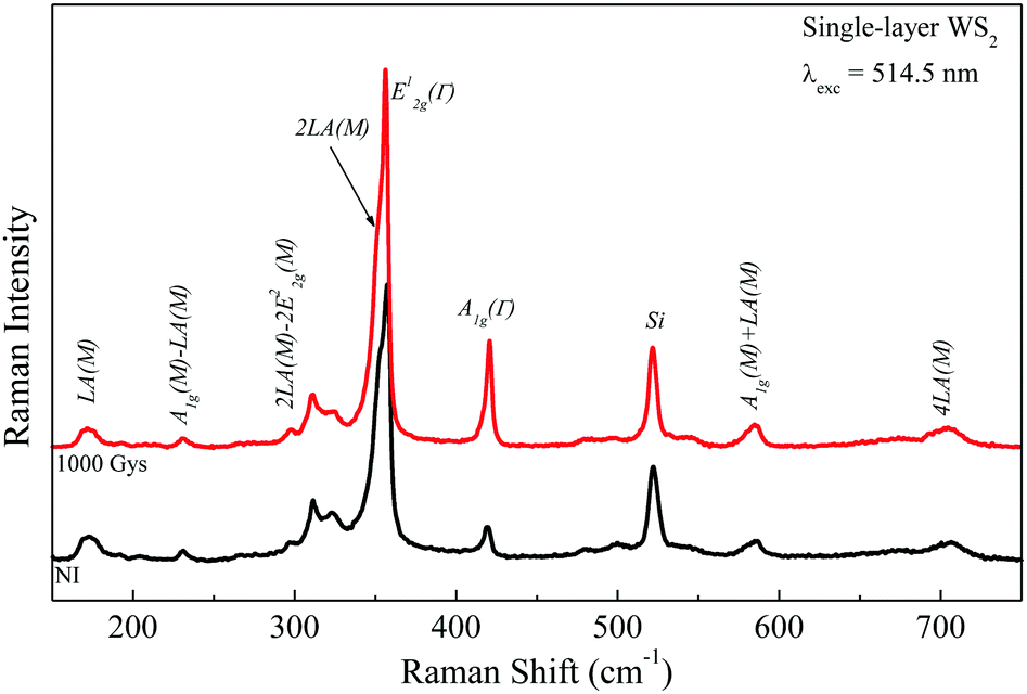 | ||
| Fig. 1 Room temperature Raman spectra of a WS2 monolayer before (non-irradiated (NI) sample, black curve) and after irradiation with 1000 Gys (red curve). | ||
However, it was found that the peak position of the A1g(Γ) and E12g(Γ) modes shifted and their relative intensities changed. Indeed, although there are a large number of provable interaction mechanisms that are known for γ-rays in semiconductor materials, Scheme 1 illustrates only some of these interactions that play a significant role in radiation measurements: photoelectric absorption, Compton scattering, pair production, vacancies and fast electrons. All of these processes might contribute to the changes of the electrical, optical and structural properties of WS2.
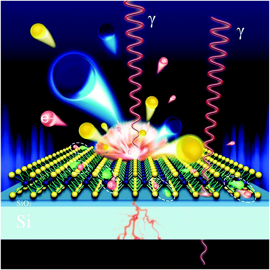 | ||
| Scheme 1 γ-ray interaction with a 2D-WS2 monolayer illustrating the generation of secondary γ photons (in the silicon substrate), electron/hole pairs, fast electrons, and creation of S and W vacancies in the monolayer. | ||
To quantitatively describe these changes, Fig. 2 shows the room temperature Raman spectra of 2D-WS2 for six different radiation doses. For clarity, the spectrum corresponding to different radiation doses is shifted vertically, and all Raman data were analyzed by multi-Lorentzian fitting to obtain the precise position of the Raman characteristic frequencies of the WS2. When the radiation intensity increases, three interesting features in irradiated samples are noticed: (i) the full width at half maximum (FWHM) of the A1g and E12g(Γ) peaks increases, see Fig. 2(a). (ii) The A1g peak shifts towards a higher wavenumber, as shown in Fig. 2(b) and (iii) the intensity ratio between A1g(Γ) and E12g(Γ) modes increases, see Fig. 2(c). The underlying physics can be understood as follows. Since high irradiation-dose gives rise to more sulfur vacancies, the p-doping concentration induced by sulfur vacancies increases.27 As a result, the FWHM of the A1g and E12g(Γ) peaks becomes broader. It is well-known, that the A1g(Γ) peak corresponds with out-of-plane vibrations of the W–S bonds with static center W atoms for the pristine system. When the radiation dose increases, on the one hand, missing a W–S bond due to an emergence of sulfur vacancies leads to a slightly reduced restoring force constant.28 On the other hand, however, the sulfur vacancies enable originally static W atoms to vibrate out of plane, which strengthens the restoring force constant from the W–S bond vibration. Competition between these two factors results in a blueshift of A1g(Γ). Besides, the irradiation induced p-doping enhances electron–phonon scattering.8 Hence it also contributes to the blueshift of A1g. Finally, the higher sensitivity of the A1g mode is attributed to its stronger electron–phonon interaction than that of the E12g(Γ) mode.27,29 It produces not only a blue shift of the A1g(Γ) peak, but also an enhancement of the ratio of IA1g/IE12g. In contrast to A1g modes, the positions of the 2LA and E12g(Γ) modes remain unchanged (see Fig. 2(a) and (b)) as radiation dose is increased.
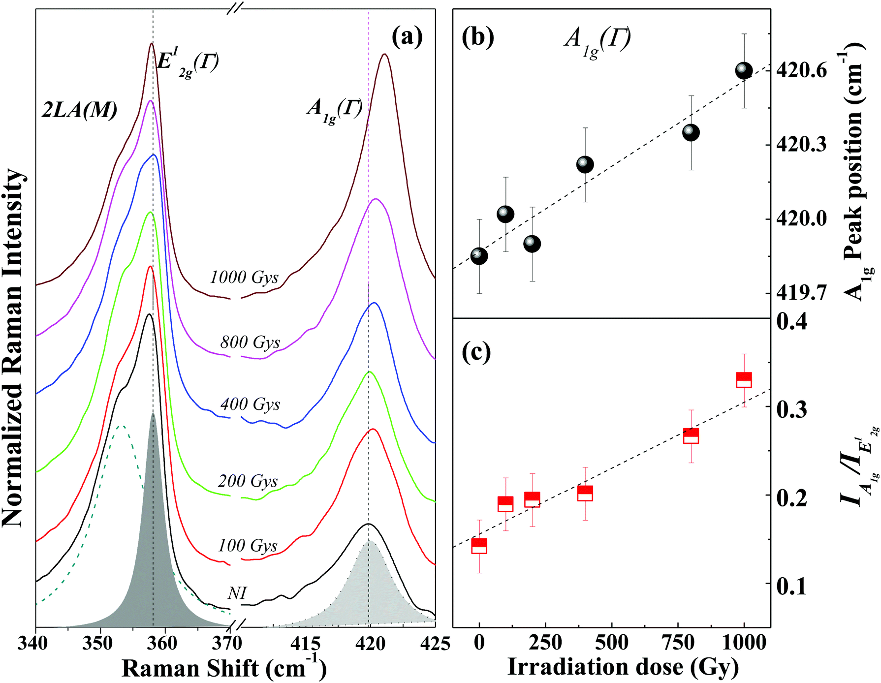 | ||
| Fig. 2 (a) Room temperature Raman spectra of WS2 samples for different radiation doses. The spectrum of the sample NI which has not been irradiated is also shown as a reference. Dashed trace, dark grey color under curve and light grey color under curve are Lorentzian fittings of three peaks, namely 2LA, A1g and E12g(Γ), respectively. (b) Peak position of A1g(Γ) and (c) intensity ratio between A1g(Γ) and E12g(Γ) as a function of radiation dose. | ||
It is worthy to recall that Raman spectroscopy could not provide a required resolution (in terms of optically active defects) for detecting the effect of small gamma radiation doses on 2D-WS2. Nevertheless, PL spectroscopy is good enough to do so.
Fig. 3(a) shows the room temperature PL spectra of 2D-WS2 samples for six different radiation doses. Note that the PL intensity is inversely proportional to radiation dose. Fig. 3(b) displays the room temperature PL spectrum of non-irradiated and irradiated (1000 Gy) 2D-WS2 samples. These PL spectra were well fitted with two Lorentzian curves, which are assigned to the neutral exciton (A0) and positively charged trion (A) emissions at 1.999 eV (highlighted in black) and 1.963 eV (highlighted in red), respectively. These energy values are in the range of reported PL peak positions for monolayer WS2.30,31 It was confirmed that the energy of the exciton and the trion did not change considerably when the radiation doses increase, as can be seen from Fig. S1 (ESI†). For this analysis, the defect-bound (D) was omitted, because at room temperature this defect is almost suppressed.
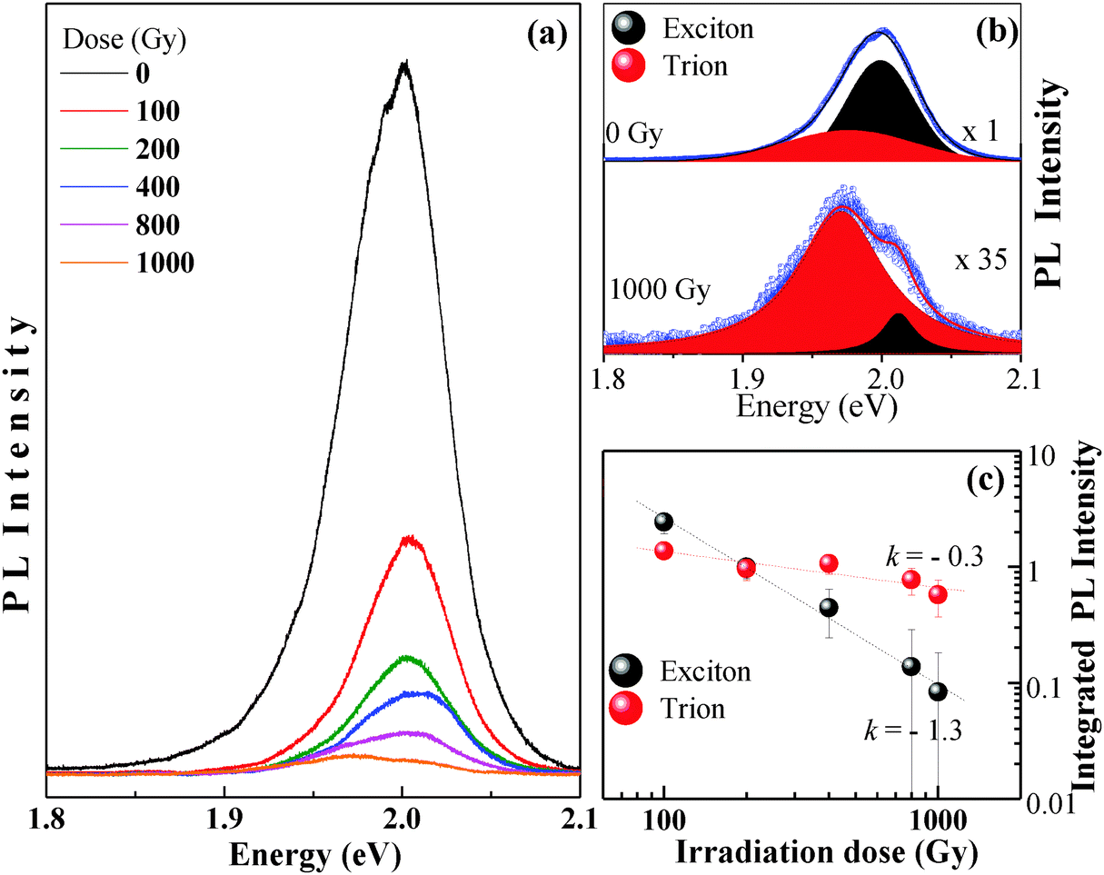 | ||
| Fig. 3 (a) Room temperature PL spectra of WS2 samples for different radiation doses. (b) Deconvolution of PL spectra of non-irradiated (upper) and irradiated (lower) (1000 Gys) 2D-WS2 samples, using the Lorentzian curves. (c) Integrated PL intensity of trions (red symbol) and excitons (black symbol) as a function of radiation dose. | ||
From the PL band deconvolution shown in Fig. 3(c) the integrated intensities related to exciton and trion emissions were obtained and plotted as a function of gamma radiation dose, and the values obtained from deconvolution of PL spectra are shown in Fig. S1 (ESI†). Note that the PL integrated intensity of both emissions decreases with increasing radiation dose. However, it is observed that the slopes (k) are k = −0.3 for the trion emission and k = −1.3 for the exciton emission. This behavior can be explained by taking into account that the defects created by the gamma radiation favours the creation of type-p vacancies, which in turn promotes the creation of trions in detriment to the creation of excitons. In a recent study, p-doping was achieved by exposing the WS2 surface to solutions of “Magic Blue”, [N(C6H4-p-Br)3]SbCl6, which acts as the oxidant. It was found that compared to the pristine WS2, the PL intensity decreases upon p-doping.27 These results indicate that hole concentrations could be controlled by gamma irradiation.
To gain an insight into the origin of the defects in 2D-WS2 created by gamma irradiation, XPS measurements have been performed on both non-irradiated and irradiated samples with doses of 100, 200, 400 and 1000 Gys, as shown in Fig. 4. The average value of the XPS measurements was obtained from three different locations on each sample for the W4f and S2p core levels. The S2p core level spectra for the non-irradiated sample (Fig. 4(a)) exhibit two peaks at 163.8 ± 0.1 eV and 162.5 ± 0.1 eV, which are attributed to the doublet S2p3/2 and S2p1/2, respectively. Fig. 4(b) displays the results of the W4f core level, where the peaks associated with the 4f7/2, 4f5/2 and 5p3/2 orbitals were localized at 32.6 eV, 34.7 eV and 37.8 eV, respectively. The energy positions of all XPS spectra are in accordance with the previously reported results for 2D-WS2.16,32,33 The peaks were fitted using a Gaussian, as shown in Fig. S2 (ESI†).
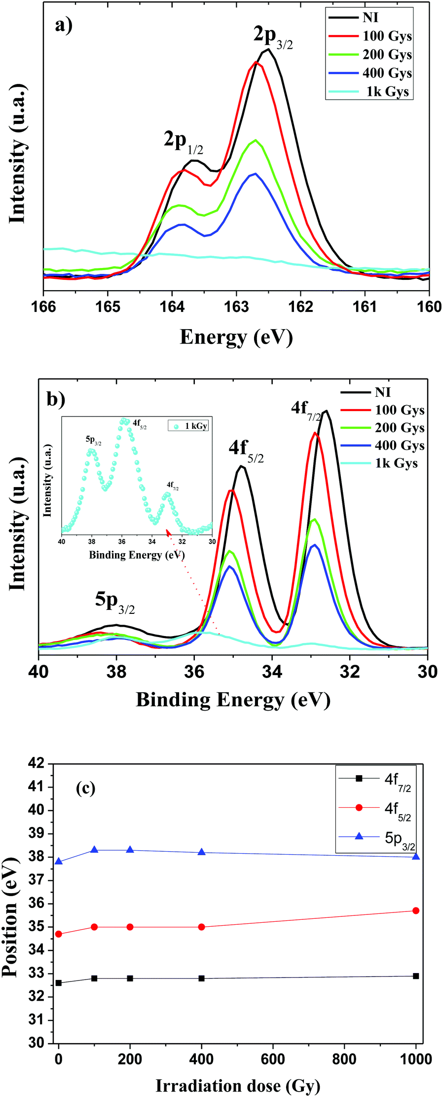 | ||
| Fig. 4 Room temperature XPS measurements for (a) S2p and (b) W4f core levels of the 2D-WS2 samples as a function of radiation dose. (c) Peak position of the 4f7/2, 4f5/2 and 5p3/2 orbitals as a function of radiation dose. The inset of (b) shows the XPS measurements for W4f core levels of the 2D-WS2 samples irradiated with 1 kGy. | ||
The spectral shape for both W and S photoemission lines for NI and irradiated samples are almost identical, which indicates that the small radiation dose does not favour the creation of an additional phase in WS2. However, it leads to about 0.2 eV shift to higher binding energy for both W and S photoemission lines, accompanied by a photoemission reduction as a function of radiation dose. At a radiation dose of 100 Gys, the 4f7/2 and 4f5/2 peaks decrease by approximately 10% with respect to their corresponding non-irradiated WS2 peak intensities. For the same radiation dose the S2p3/2 and S2p1/2 peak intensity decreases by approximately 7.0%. For samples submitted to the dose of 400 Gys, however, the intensity of the peaks of both W and S photoemission lines decreases by about 55% from their corresponding non-irradiated WS2 peak intensity. From Fig. 4(a) and (b), it is also notable that there is a tendency to reduce the signal intensity of both sulfur and tungsten sites in the irradiated samples. There are two reasons responsible for this behavior: (i) the number of S and W sites across the monolayer WS2 surface decreases considerably with increasing radiation dose; (ii) the second and most dominant effect is the existence of an ionization process. The evidence of this second reason is demonstrated in the inset of Fig. 4(b), where the ratio between the innermost orbitals and outermost orbitals of W increases with the dose of 1 kGy. Additionally, for this same sample no XPS signal was detected for sulfur orbitals (2p3/2 and S2p1/2). However, this does not mean that there are no sulfur atoms in the WS2 monolayer, since they were observed in Raman and PL spectra shown in Fig. 1–3 for the 2D-WS2 sample irradiated with 1 kGy. Thus, gamma radiation might create active defects in the 2D-WS2 and a doping process may be occurring.
Magnetic properties in NI and irradiated samples have been studied by carrying out field (H) dependant magnetisation (M) measurements, as depicted in Fig. 5(a). The diamagnetic contribution originating from the sample holder has been removed.
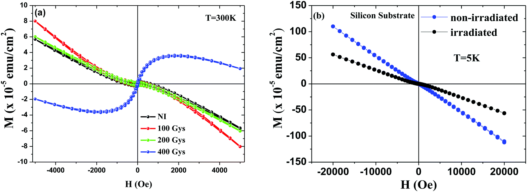 | ||
| Fig. 5 Magnetization versus magnetic field for (a) pristine 2D-WS2 samples as a function of radiation dose at 300 K. (b) SiO2/Si substrate before and after gamma radiation (400 Gys) at 5 K. | ||
For the NI sample and samples irradiated with 100, 200 and 1000 Gys (not shown here) a dominant diamagnetic behaviour is observed. The 2D-WS2 irradiated with 400 Gys exhibits, however, a hysteresis loop with finite coercivity (37 Oe) and remanence (2.5 × 10⁻⁶ emu cm−2) which is a signature of ferromagnetism. To eliminate a possible existence of magnetism that could originate from any impurities due to radiation or some contamination of the substrates, M vs. H measurements were performed on the substrate before and after gamma irradiation at 5 K. As shown in Fig. 5(b) both the non-irradiated and irradiated substrate exhibit a diamagnetic response. This indicates that the ferromagnetism observed in M vs. H emanates from the TMDC monolayer, rather than the substrate. Therefore, one could affirm that the ferromagnetism (FM) is unique to a 2D-WS2 irradiated sample with 400 Gys dose. In addition, other different pieces of the sample irradiated at 400 Gys also show the FM characteristic. Thus, one can conclude that the FM behaviour is attributed to vacancies of sulfur and tungsten atoms and the higher density of defects created by ionizing irradiation. This is also confirmed by DFT calculations. In addition, at T = 5 K a similar FM behaviour observed in 2D-WS2 irradiated with 400 Gys dose, which confirms that the magnetic characteristic of the sample is due to the defects (not shown here), provides further evidence of our conclusion. Indeed, these results are consistent with XPS results, where the intensities of the peaks due to both W and S photoemission lines for the 2D-WS2 irradiated sample with 400 Gys decrease about 55% from their corresponding non-irradiated WS2 peak intensities.
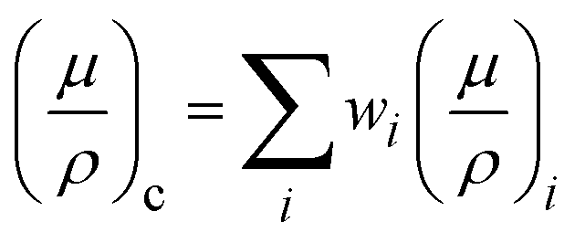
Our results open up a new possibility to develop high-sensitivity gamma detectors based on 2D-WS2 materials, since gamma radiation can create electrically active defects. Actually, gamma-ray detectors are manufactured from ultrapure germanium, which are usually called high-purity germanium (HPGe) detectors, i.e. the impurity concentration in germanium is approximately 1010 atoms per cm3, which makes these devices based on this high-purity material have a depletion depth of several centimeters.34 On the other hand, devices based on VdWE-grown 2D WS2 monolayers may have high detection performance and reduced size as will be explained below. The interaction probability between monoenergetic gamma rays and the absorber WS2 can be obtained from
| P = 1 − e−(μ/ρ)ρt |
where wi represents the weight fraction of element i (W, S). γ-ray attenuation plotted in Fig. S3 (ESI†) was calculated using XCOM (Photon Cross Sections Database),35 which is based on the above equations. Thus, photon attenuation for both MoS2 and WS2 due to photoelectric absorption and the total attenuation (where different interaction mechanisms are involved) are shown in Fig. S3 (ESI†). Since molybdenum disulfide (MoS2) is one of the most studied materials in the TMDC family,36 we have chosen it for comparison with WS2 in terms of the attenuation process of γ-rays. Additionally, as most of the contribution of scattering in TMDCs is due to photoelectric absorption, we choose it for comparison purposes. As can be seen from Fig. S3 (ESI†), the WS2 material possesses a photoelectric absorption higher than MoS2. These results show that WS2 has stronger radiation interaction than that of MoS2. Therefore, from the device applications point of view, such as dosimeters and radiation sensors, a better performance would be expected from WS2 based devices. Finally, our results showed a fascinating effect of gamma radiation on 2D-WS2. This is related to the control of p-doping concentration in a VdWE-grown monolayer of WS2 using gamma radiation by creating W defects. A similar result has been reported for graphene, where gamma radiation was used to p-dope graphene.37 Several reports have demonstrated that gamma radiation treatments modify the material properties by the self-controlled process and this characteristic effect can be used to develop materials with statistically stabilized and desired properties.38,39
In order to gain a deep insight into the origin of the magnetization observed in the monolayer WS2, as shown in Fig. 5(a), we performed DFT calculations using the projector-Augmented-wave method implemented in the Vienna ab initio simulation package (VASP).40,41 The Perdew–Burke–Ernzerhof form of the generalized-gradient-approximation exchange–correlation functional was adopted. The original 4 × 4 × 1 supercell (48 atoms) is selected as the sheet for the sample with vacancies; for further details see Fig. S5 (ESI†). In order to reduce the interactions between the periodic structures in the vertical direction, a 15 Å vacuum is added in the construction of the model. The cutting energy of the plane wave is set to 400 eV. When the structure relaxes, the convergence precision of each interatomic force is 0.01 eV Å−1, and the self-consistent convergence energy is not higher than 10−4 eV.
The Brillouin zone is summed according to the 5 × 5 × 1 Monkhorst–Pack K point. The spin density is defined as Δρs = ρ↑ − ρ↓, in which ρ↑ and ρ↓ denote the spin-up and spin-down charge density, respectively. It is well-known that the simplest and most abundant defects in TMDCs are vacancies. To get complete information about the origin of the magnetism, several different types of point defects are proposed in our DFT calculations, including mono-sulfur vacancy (V1S), double sulfur vacancies (V2S), mono-tungsten vacancy (V1W), vacancy complex of one W and one nearby sulfur (V1W+1S), vacancy complex of one W and a pair of nearby sulfurs (V1W+2S), etc. In addition, in the case of V1W+2S, for a given W vacancy, ten different positions of the S pairs are considered. It is found that V1S possesses the lowest formation energy of these defects. Hence, when the sample is irradiated by gamma rays, the V1S vacancies are created, as discussed in the previous sections. However, the presence of an S vacancy does not induce polarization of either the density of states (DOS) or spin density. Hence the total magnetic moment of the system is zero. Even though the concentration of V1S vacancies is increased or there are other types of S vacancies existing such as V2S, the situation still remains unchanged. Similarly, the V1W alone also does not induce magnetism in a WS2 monolayer, because each W vacancy can extract four electrons from the system, resulting in p-type doping. Amongst them, two electrons occupy the spin-up channel and two occupy the spin-down channel. Therefore, no magnetism is expected. Nevertheless, the situation changes when the vacancy complex of V1W+2S emerges.
Fig. 6 depicts the band structures and the DOS of the perfect WS2 monolayer and the system contains V1W+2S defects. From Fig. 6(b), notice that the DOS of the spin-up and spin-down states is completely symmetrical for the perfect system, namely, spin is unpolarized. Then the total magnetic moment of the perfect monolayer WS2 is zero. Compared to the perfect sample (Fig. 6(a)), some impurity states appear in the gap of the V1W+2S system, see Fig. 6(c). The local moment stemming from the p-orbital of the S atoms and the d-orbital of W atoms gives rise to an asymmetric spin-up and spin-down DOS near the Fermi energy, as shown in Fig. 6(d). In addition, the strong spin polarization is also clearly exhibited in the isosurface plot of the spin density in real space, see the red and green isosurfaces in Fig. 6(e) which represent positive and negative spin densities, respectively. It is this localized spin polarization that leads to the formation of the magnetic moment in the system with magnetic moment of 2.0 μB.
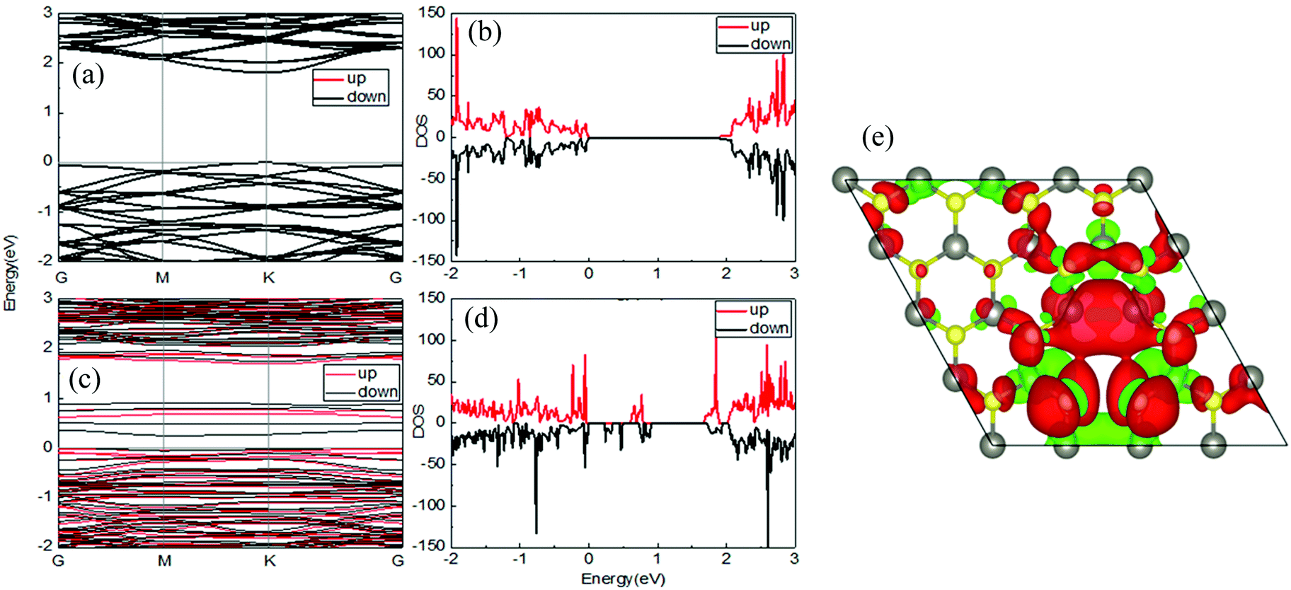 | ||
| Fig. 6 Band structure (a) and density of states (DOS) (b) of a perfect WS2 monolayer. Band structure (c) and DOS (d) of the system with a vacancy complex of one W and a pair of its nearby sulfurs in the upper and lower layers at the A site. The red and black curves correspond to spin-up and spin-down states. (e) Spin density distributions of this system with a vacancy complex of W and nearby one sulfur pair in the upper and lower layers at the A site in real space. Red and green iso-surfaces represent positive and negative spin densities, respectively. | ||
Relating this theoretical prediction with experimental data, one infers that gamma irradiation might create either V1S, V2S, V1W or V1W+2S vacancies. In the small radiation dose, the V1S vacancies are predominant. With increasing radiation intensity, the V1W+2S vacancies might also start to play a role in the magnetic properties of WS2 monolayers. Then at large radiation dose the magnetization is expected, which is consistent with experimental data.
Experimental
In this work large-scale (10 mm by 10 mm) WS2 monolayers were grown by a van der Waals epitaxy (VdWE) process on 280 nm thick thermal oxide (SiO2) coated silicon substrates.21 The original sample grown on a SiO2/Si substrate was cut into smaller pieces, and each piece was sealed in an acrylic box and irradiated with different doses of gamma radiation. A non-irradiated sample, labelled NI was used as a reference sample. Each sample was irradiated with 100, 200, 400, 800, and 1000 Gys, in a gamma-cell irradiator model 220 Excel from MDS Nodion company (60Co 2.7 kGy h−1). The XPS measurements were performed in a Thermo K-Alpha XPS from Thermo Scientific Inc. fitted with a monochromatic X-ray source with an Al anode of energy Ka = 1486 eV. Raman spectra were obtained with a JY-T64000 micro-Raman spectrometer using the 514.5 nm excitation line of an Argon laser through a 50× objective, resulting in a laser spot of around 1.5 μm in diameter in the focal plane. Macro-PL measurements were performed as a function of temperature and radiation dose using an Argon laser tuned at 514 nm. All PL and Raman measurements were performed at low laser powers, thus avoiding any heating effects on the monolayer films. DC magnetization (MT) measurements were carried out using a 7![[thin space (1/6-em)]](https://www.rsc.org/images/entities/char_2009.gif) T Quantum design SQUID-VSM.
T Quantum design SQUID-VSM.
Conclusions
In summary, we have demonstrated experimentally that gamma irradiation dramatically affects the physical properties of monolayer WS2 such as a blue shift of the A1g(Γ) peak, an increase of the intensity ratio between A1g(Γ) and E12g(Γ) modes and an enhancement of the trion emission intensity. This indicates that the irradiation creates vacancies and induces effective p-doping. Remarkably, in monolayer WS2, we find a gamma radiation induced magnetic phase transition from diamagnetic to a ferromagnetic phase at both room temperature and low temperature. First principles calculations illustrate that the magnetism stemmed from the complex vacancies composed of one tungsten and a pair of its nearby sulfurs, providing further support for our conclusions. In addition, we also showed that the monolayer WS2 possesses a high-performance for the detection of low doses of gamma ray radiation. Finally, these exotic effects of gamma radiation will stimulate the development of radiation sensors of gamma rays based on 2D-WS2 materials.Conflicts of interest
There are no conflicts to declare.Acknowledgements
We would like to thank the Brazilian agencies CNPq, CAPES, and FAPDF (grant number: 193.001.757/2017) for financial support and the research scholarship. We also would like to thank the Brazilian Nanotechnology National Laboratory for XPS measurements. The 2D materials work is partly funded through the Future Photonics Manufacturing Hub (EPSRC EP/N00762X/1) and the Chalcogenide Photonic Technologies (EPSRC EP/M008487/1) at the University of Southampton, United Kingdom.References
- W. Choi, N. Choudhary, G. H. Han, J. Park, D. Akinwande and Y. H. Lee, Mater. Today, 2017, 20, 116 CrossRef CAS.
- W. Wu, Q. Zhang, X. Zhou, L. Li, J. Su, F. Wang and T. Zhai, Nano Energy, 2018, 51, 45 CrossRef CAS.
- K. G. Zhou and H. L. Zhang, Small, 2015, 11, 3206 CrossRef CAS PubMed.
- P. Miró, M. Ghorbani-Asl and T. Heine, Angew. Chem., Int. Ed., 2014, 53, 3015 CrossRef.
- J. Theerthagiri, K. Karuppasamy, G. Durai, A. ul H. S. Rana, P. Arunachalam, K. Sangeetha, P. Kuppusami and H.-S. Kim, Nanomaterials, 2018, 8, 256 CrossRef.
- S.-L. Li, K. Tsukagoshi, E. Orgiu and P. Samor, Chem. Soc. Rev., 2016, 45, 118 RSC.
- O. Zheliuk, J. Lu, J. Yang and J. Ye, Phys. Status Solidi RRL, 2017, 11, 1700245 CrossRef.
- M. W. Iqbal, M. Z. Iqbal, M. F. Khan, M. A. Shehzad, Y. Seo and J. Eom, Nanoscale, 2015, 7, 747 RSC.
- W. Zhao, Z. Ghorannevis, L. Chu, M. Toh, C. Kloc, P.-H. Tan and G. Eda, Nanoscale, 2012, 7, 791 Search PubMed.
- B. Zhu, H. Zeng, J. Dai, Z. Gong and X. Cui, Proc. Natl. Acad. Sci. U. S. A., 2014, 111, 11606 CrossRef CAS.
- C. Jin, J. Kim, M. I. B. Utama, E. C. Regan, H. Kleemann, H. Cai, Y. Shen, M. James Shinner, A. Sengupta, K. Watanabe, T. Taniguchi, S. Tongay, A. Zettl and F. Wang, Science, 2018, 360, 893 CrossRef CAS.
- S. Lepeshov, M. Wang, A. Krasnok, O. Kotov, T. Zhang, H. Liu, T. Jiang, B. Korgel, M. Terrones, Y. Zheng and A. Alu, ACS Appl. Mater. Interfaces, 2018, 10, 16690 CrossRef CAS PubMed.
- Y. Yue, J. C. Chen, Y. Zhang, S. S. Ding, F. Zhao, Y. Wang, D. Zhang, R. J. Li, H. Dong, W. Hu, Y. Feng and W. Feng, ACS Appl. Mater. Interfaces, 2018, 10, 22435 CrossRef CAS.
- A. Yoshimura, M. Lamparski, N. Kharche and V. Meunier, Nanoscale, 2018, 10, 2388 RSC.
- P. Atkin, D. W. M. Lau, Q. Zhang, C. Zheng, K. J. Berean, M. R. Field, J. Z. Ou, I. S. Cole, T. Daeneke and K. Kalantar-zadeh, 2D Mater., 2018, 05, 015013 CrossRef.
- L. Ma, Y. Tan, M. Ghorbani-Asl, R. Boettger, S. Kretschmer, S. Zhou, Z. Huang, A. V. Krasheninnikov and F. Chen, Nanoscale, 2017, 9, 11027 RSC.
- H. Song, X. Yu, M. Chen, M. Qiao, T. Wang, J. Zhang, Y. Liu, P. Liu and X. Wang, Appl. Surf. Sci., 2018, 439, 240 CrossRef CAS.
- A. Y. Polyakov, S. J. Pearton, P. Frenzer, F. Ren, L. Liu and J. Kim, J. Mater. Chem. C, 2013, 1, 877 RSC.
- B. Fraboni, A. F. Morgera and N. Zaitseva, Adv. Funct. Mater., 2016, 26, 2276 CrossRef CAS.
- R. C. Walker, T. Shi, B. Jariwala, I. Jovanovic and J. A. Robinson, Appl. Phys. Lett., 2017, 111, 143104 CrossRef.
- V. O. Gordo, M. A. G. Balanta, Y. G. Gobato, F. S. Covre, F. Iikawa, O. D. D. Couto, F. Qu, H. V. A. Galeti, M. Henini, D. W. Hewak and C. C. Huang, Nanoscale, 2018, 10, 4807 RSC.
- A. C. Ferrari, J. C. Meyer, V. Scardaci, C. Casiraghi, M. Lazzeri, F. Mauri, S. Piscanec, D. Jiang, K. S. Novoselov, S. Roth and A. K. Geim, Phys. Rev. Lett., 2006, 97, 187401 CrossRef CAS.
- Z. He, X. Wang, W. Xu, Y. Zhou, Y. Sheng, Y. Rong, J. M. Smith and J. H. Warner, ACS Nano, 2016, 10, 5847 CrossRef CAS.
- A. A. Mitioglu, P. Plochocka, G. Deligeorgis, S. Anghel, L. Kulyuk and D. K. Maude, Phys. Rev. B: Condens. Matter Mater. Phys., 2014, 89, 245442 CrossRef.
- A. Berkdemir, H. R. Gutiérrez, A. R. B. Méndez, N. P. López, A. L. Elías, C.-I. Chia, B. Wang, V. H. Crespi, F. L. Urías, J.-C. Charlier, H. Terrones and M. Terrones, Sci. Rep., 2013, 175, 1 Search PubMed.
- J. Gabrusenoks, A. Veispals, A. von Czarnowski and K.-H. Meiwes-Broer, Electrochim. Acta, 2001, 46, 2229 CrossRef CAS.
- Z. Wu and Z. Ni, Nanophotonics, 2017, 6, 1219 CAS.
- S. Zhang, H. M. Hill, K. Moudgil, C. A. Richter, A. R. H. Walker, S. Barlow, S. R. Marder, C. A. Hacker and S. J. Pookpanratana, Adv. Mater., 2018, 30, 1802991 CrossRef.
- J. D. Lin, C. Han, F. Wang, R. Wang, D. Xiang, S. Qin, X.-A. Zhang, L. Wang, H. Zhang, A. T. S. Wee and W. Chen, ACS Nano, 2014, 8, 5323 CrossRef CAS.
- Y. Lee, G. Ghimire, S. Roy, Y. Kim, C. Seo, A. K. Sood, J. I. Jang and J. Kim, ACS Photonics, 2018, 5, 2904 CrossRef CAS.
- H. R. Gutiérrez, N. P. López, A. L. Elías, A. Berkdemir, B. Wang, R. Lv, F. L. Urías, V. H. Crespi, H. Terrones and M. Terrones, Nano Lett., 2013, 13, 3447 CrossRef.
- G. Pagona, C. Bittencourt, R. Arenal and N. Tagmatarchis, Chem. Commun., 2015, 51, 12950 RSC.
- J.-G. Song, J. Park, W. Lee, T. Choi, H. Jung, C. W. Lee, S.-H. Hwang, J. M. Myoung, J.-H. Jung, S.-H. Kim, C. L. Matras and H. Kim, ACS Nano, 2013, 7, 11333 CrossRef CAS.
- G. F. Knoll, Radiation detection and measurement, Wiley, Hoboken, NJ, USA, 4th edn, 2010 Search PubMed.
- M. J. Berger, J. H. Hubbell, S. M. Seltzer, J. Chang, J. S. Coursey, R. Sukumar, D. S. Zucker and K. Olsen, NIST Stand. Ref. Database, 1998, 8, 87 Search PubMed.
- R. Addou, L. Colombo and R. M. Wallace, ACS Appl. Mater. Interfaces, 2015, 7, 11921 CrossRef CAS.
- K. Alexandrou, A. Masurkar, H. Edrees, J. F. Wishart, Y. Hao, N. Petrone, J. Hone and I. Kymissis, Appl. Phys. Lett., 2016, 109, 153108 CrossRef.
- I. Zadorozhnyi, J. Li, S. Pud, H. Hlukhova, V. Handziuk, Y. Kutovyi, M. Petrychuk and S. Vitusevich, Small, 2018, 14, 1702516 CrossRef.
- J. Guo, Y. Li, S. Wu and W. Li, Nanotechnology, 2005, 16, 2385 CrossRef CAS.
- G. Kresse and J. Furthmüller, Comput. Mater. Sci., 1996, 6, 15 CrossRef CAS.
- G. Kresse and D. Joubert, Phys. Rev. B: Condens. Matter Mater. Phys., 1999, 59, 1758 CrossRef CAS.
Footnote |
| † Electronic supplementary information (ESI) available. See DOI: 10.1039/c9nh00414a |
| This journal is © The Royal Society of Chemistry 2020 |