
Will surface effects dominate in quasi-two-dimensional gallium oxide for electronic and photonic devices?
Jihyun
Kim
 *a,
F.
Ren
b and
S. J.
Pearton
c
*a,
F.
Ren
b and
S. J.
Pearton
c
aDepartment of Chemical and Biological Engineering, Korea University, Anam-dong, Sungbuk-gu, Seoul 02841, South Korea. E-mail: hyunhyun7@korea.ac.kr
bDepartment of Chemical Engineering, University of Florida, Gainesville, Florida 32611, USA
cDepartment of Materials Science and Engineering, University of Florida, Gainesville, Florida 32611, USA
First published on 6th June 2019
Abstract
There is currently great interest in ultra-wide bandgap semiconductors for their applicability in power switching electronics with improved efficiency compared to current technologies and also to solar-blind UV detection. One of the most promising materials is Ga2O3, available in large area bulk crystals and as exfoliated nano-layers (nanobelts, nanomembranes, and nanosheets). One aspect of this material that has not been widely recognized is the sensitivity of its surface to environment. The goal of this brief focus article is to provide some insight into the mechanisms and defects that underlie this effect and explain inconsistencies in the literature.
Gallium oxide has a number of polymorphs, with the β- and α-variants emerging as next-generation ultra-wide bandgap semiconductors (bandgap 4.6–4.8 eV for β and ∼5.2 eV for α-polymorphs).1–3 These have the potential for transformative impact on the energy economy, due to their more efficient power switching capabilities in power control and conversion applications such as in the automotive industry, data center power management, grid control, and industrial and locomotive traction control.1–4 However, a high density of crystal defects in the bulk of Ga2O3 significantly hinders the progress in realizing many of the beneficial attributes of power electronics systems.4 What is less commonly realized is that surface effects are also very important with Ga2O3, a factor that has been overlooked in a previous review of its research challenges.4
Despite not being a van der Waals material and having very strong ionic bonding, the more commonly studied β-phase can be mechanically cleaved and exfoliated easily along favorable surfaces.2,3 The large anisotropy of the lattice constant in this monoclinic phase allows a facile cleavage (a[100] = 12.225 Å, b[010] = 3.039 Å, and c[001] = 5.801 Å) along the (100) and (001) faces. From bond strength calculations, the surface covalent bonds in these planes are up to 6 eV per bond stronger than the perpendicular bonds, which break easily.5 Thin quasi-2D nano-layers (nanobelts, nanomembranes, and nanosheets) can be exfoliated from bulk crystals, similar to true 2D materials such as graphene or MoS2,6,7 and used to fabricate transistor and photodetector structures.8 In addition, single-crystalline ultrathin quasi-hexagonal (010) β-Ga2O3 nanosheets can be homoepitaxially grown on nanowire seeds.9 The fabrication of devices using β-Ga2O3 nanobelts has several advantages over conventional bulk single crystals, including the absence of strain and the fact that the heat management problem related to the low thermal conductivity1–3 of β-Ga2O3 can be mitigated by applying it to substrates with high thermal conductivity.
The surface termination, relaxation and surface energies for different faces of β-Ga2O3 have been reported by Bermudez10 and provide insight into the structure of nanosheets. Fig. 1 shows schematics of the ideally terminated (100)-A and (100)-B surfaces. A and B refer to two possible terminations, corresponding to stoichiometric unit cells with non-polar surfaces. A refers to termination in rows of O(II)s lying along the [0 1 0] direction with each O(II) back-bonded to two Ga(I)s. B refers to termination in nearest-neighbor rows of Ga(II) and O(III) atoms, each singly-unsaturated, with full coordination of Ga(I) and O(I) atoms at the surface. Hartree–Fock calculations show that the (100)-B surface has the lowest surface energy under both the ideal (0.96 J m−2) and relaxed (0.68 J m−2) conditions, while the (010) surface has the highest surface energy under the relaxed condition.10 Experimental data show that Ga2O3 powders have equivalent surface and bulk compositions, without favorable surface stabilization.11,12 Collins et al.11 reported that H2 is dissociatively chemisorbed, following reaction pathways involving endothermal dissociation occurring over surface Ga sites at T > 450 K, producing Ga–H(I) bonds (heat and entropy of this hydrogen adsorption were ΔhI = 155 ± 25 kJ mol−1 and ΔsI = 0.27 ± 0.11 kJ mol−1 K−1). An additional pathway present at low temperatures involves surface Ga–O–Ga species, producing GaO–H and Ga–H(II) bonds that are stable after heating under vacuum at T > 650 K. It has long been established that oxygen vacancies are produced during heating under vacuum,12 where the relationship between conductivity (σ) and O2 partial pressure (pO2) is given by σ ∼ (pO2)−0.25.
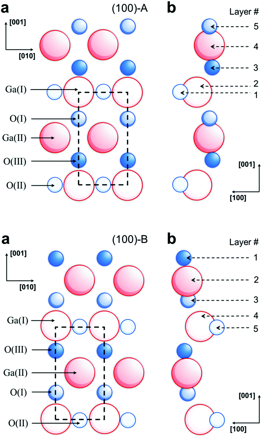 | ||
| Fig. 1 Schematic representation of ideally terminated (1 0 0)-A (top) and (100)-B surfaces of β-Ga2O3. (a) View along surface normal-dashed lines show the surface unit cell; (b) outermost surface layers, viewed along the [0 1 0] direction, with vectors indicating the displacements occurring during relaxation. The displacement vectors are increased by a factor of 4 relative to the interatomic distances. All displacements are in the plane of the page, i.e., the (0 1 0) plane (after Bermudez9). | ||
While the possible thickness-dependent bandgap and mobility at the nanoscale limit13 have not been well understood in Ga2O3, the nanobelts can also be integrated with other low-dimensional materials, taking advantage of quasi-2D structures, including h-BN, to fabricate metal–insulator–semiconductor field effect transistors.8,14–17 Zhou et al.16 fabricated nanobelt devices with various thicknesses and found that the threshold voltage (VT) shifted from negative to positive as the thickness was decreased. Enhancement-mode (E-mode) β-Ga2O3 nanobelt FETs demonstrated a breakdown voltage of 185 V with negligible hysteresis and a high on/off ratio, promising for future power devices.8 There are also extensive studies of solar-blind UV photodetectors fabricated on Ga2O3 nanobelts.8
There are also more speculative potential applications, including resistive-RAM (ReRAM or RRAM), a non-volatile memory gaining attention because it can be utilized to build neuromorphic computing chips.18 Many metal oxides have been investigated in this regard because the oxygen ions and oxygen vacancies can easily drift under an electric field. The motion of oxygen ions and oxygen vacancies needs to be investigated in β-Ga2O3 nano-layers, but memristic behavior has been observed.19–21 Heterojunction Bipolar Transistors (HBTs) using nano-layer β-Ga2O3 as the emitter have great potential because the physical stacking of the exfoliated layers can offer the ideal structure of HBTs without considering the lattice matching.22 Finally, ultra-thin β-Ga2O3 can offer a more robust radiation-hard platform because of the lower chance for damage accumulation. Most high energy particles which commonly cause lethal damage to electronic devices can penetrate through the active area of the nano-scale devices, which is advantageous over the conventional thin-film devices. Monolithic integration of β-Ga2O3-based diodes, transistors, gas sensors, solar-blind photodetectors, HBTs, inverters, logic devices, and resistive random access memory (ReRAM) can be demonstrated in β-Ga2O3 nanodevices, which will be robust in a harsh environment.23
However, it is not widely appreciated that the surface of β-Ga2O3 is strongly affected by exposure to gaseous or plasma environments and the influence of changing conductivity and role of surface states in oxidizing or reducing environments are not established. This is despite the fact that gallium oxide diodes are known to be sensitive detectors of hydrogen.23 Swallow et al.24 reported that as-grown (![[2 with combining macron]](https://www.rsc.org/images/entities/char_0032_0304.gif) 01) single crystals exhibit electron accumulation at the surface, producing downward band bending, ascribed to negatively charged acceptor-type intrinsic surface states. Removal of OH species from the surface shifted the valence band maximum by roughly 0.5 eV and electrons accumulated, causing upward band bending. Other electronic oxides, including ZnO and SnO2 can also exhibit either surface electron accumulation or depletion and this has been ascribed to the differences in cation/anion size and electronegativity.25,26 Photoemission experiments in Ga2O3 have typically suggested surface electron accumulation,27 but the role of cleaning and annealing, processes inherent to actual device processing, indicates a more complex behavior.24,28 For example, F plasma exposure leads to compensation of near-surface donors by F− ions and significant changes in Fermi level pinning.28
01) single crystals exhibit electron accumulation at the surface, producing downward band bending, ascribed to negatively charged acceptor-type intrinsic surface states. Removal of OH species from the surface shifted the valence band maximum by roughly 0.5 eV and electrons accumulated, causing upward band bending. Other electronic oxides, including ZnO and SnO2 can also exhibit either surface electron accumulation or depletion and this has been ascribed to the differences in cation/anion size and electronegativity.25,26 Photoemission experiments in Ga2O3 have typically suggested surface electron accumulation,27 but the role of cleaning and annealing, processes inherent to actual device processing, indicates a more complex behavior.24,28 For example, F plasma exposure leads to compensation of near-surface donors by F− ions and significant changes in Fermi level pinning.28
A number of authors have shown that annealing Ga2O3 in O2versus N2 environments produces a pronounced reduction in near-surface n-type carrier concentration.3,29 Annealing of undoped Ga2O3 in an oxidizing atmosphere at ≥1200 °C for extended periods (>20 h) decreases the bulk free electron concentration by about one order of magnitude, while the surface becomes insulating.3 Moreover, the semiconducting behavior of the surface was recovered by annealing in a H2-containing reducing atmosphere. The surface conductivity could be reversibly changed by one order of magnitude by only annealing, while the surface of the bulk crystals could be reversibly switched between semiconducting and insulating by annealing in oxidizing and reducing atmospheres.3,24
These large swings in near-surface and bulk conductivity will be prohibitive in achieving stable operation of nanobelt devices unless the defects responsible are understood and effective passivation schemes are developed. At a minimum, it is already clear that O2, N2, H2 and F2 exposure can dramatically alter the near-surface conductivity.
Native point defects in β-Ga2O3 include Ga vacancies (VGa) at tetrahedral (Ga1) and octahedral (Ga2) sites, as well as oxygen vacancies at threefold coordinated sites (O1 and O2) and fourfold coordinated sites (O3).30,31 In most metal oxides, the cation vacancies and oxygen interstitials tend to be acceptors,6,7 while the oxygen vacancies and cation interstitials are donors. In n-type Ga2O3, the gallium vacancy in Ga2O3 is a triple acceptor, the oxygen interstitial (Oi) is neutral, and the gallium interstitials (Gai) are in the![[thin space (1/6-em)]](https://www.rsc.org/images/entities/char_2009.gif) 3+ charge state.30,31 The calculated oxygen vacancy (VO) formation energies of 2.7–3.6 eV suggest that they are deep donors and will be neutral in highly n-type materials and do not directly contribute to the electrical conductivity.31 Oxygen vacancies occur as neutral (VO) and double ionized vacancies (VO2−) with VO dominating at low oxygen partial pressure.3 Gallium vacancies (VGa) form triple acceptors at 3− charge state, between 1.6 and 1.8 eV below the conduction band minimum for VGa1 and VGa2,30,31 respectively, and are deep acceptors. The VGa concentration increases with oxygen partial pressure, leading to a conductivity compensation. The influence of environment on the diffusion and complexing of these defects with other defects or impurities in Ga2O3 is not currently understood. Fig. 2 shows a schematic of the β-Ga2O3 lattice structure, containing Ga and O vacancies and the typical ambient species present during processes such as annealing during device fabrication.
3+ charge state.30,31 The calculated oxygen vacancy (VO) formation energies of 2.7–3.6 eV suggest that they are deep donors and will be neutral in highly n-type materials and do not directly contribute to the electrical conductivity.31 Oxygen vacancies occur as neutral (VO) and double ionized vacancies (VO2−) with VO dominating at low oxygen partial pressure.3 Gallium vacancies (VGa) form triple acceptors at 3− charge state, between 1.6 and 1.8 eV below the conduction band minimum for VGa1 and VGa2,30,31 respectively, and are deep acceptors. The VGa concentration increases with oxygen partial pressure, leading to a conductivity compensation. The influence of environment on the diffusion and complexing of these defects with other defects or impurities in Ga2O3 is not currently understood. Fig. 2 shows a schematic of the β-Ga2O3 lattice structure, containing Ga and O vacancies and the typical ambient species present during processes such as annealing during device fabrication.
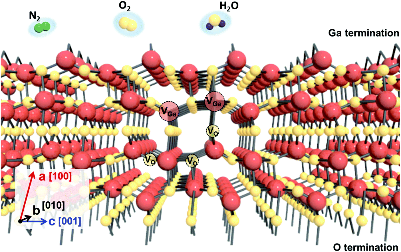 | ||
| Fig. 2 β-Ga2O3 lattice structure showing the presence of O and Ga vacancies and ambient molecules that can affect surface conductivity. | ||
The configurations of hydrogen in the bulk of β-Ga2O3 are now clearer,32 but the expected donor nature of interstitial hydrogen may be modified in the presence of surface oxygen atoms.19 All this suggests that variations in the gas atmosphere used during processing by different groups will continue to lead to large variations in reported device performance. Trap spectral measurements show that exfoliated β-Ga2O3 inherits the characteristics of the single-crystal β-Ga2O3 from which it was separated.33 Thus the control of defects and impurities in the starting substrate is also key. Optimized passivation layers for β-Ga2O3 nanobelts are required to enhance the stability of these devices because the properties are affected by environmental conditions.
In summary, in this Focus Article, we have provided examples of significant changes in the electronic nature of Ga2O3 surfaces, and briefly mentioned mechanisms that affect these quantities as well as some techniques to mitigate them. This article should be considered as a short introduction to the vast literature that covers these topics in great depth.
Conflicts of interest
There are no conflicts to declare.Acknowledgements
The work at Korea University was supported by the Korea Institute of Energy Technology Evaluation and Planning (KETEP), with granted financial resource from the Ministry of Trade, Industry and Energy, Korea (No. 20172010104830). The work at UF is partially supported by HDTRA1-17-1-0011 (Jacob Calkins, monitor) and also by NSF DMR 1856662 (Tania Paskova).References
- M. Higashiwaki and G. H. Jessen, Guest Editorial: The dawn of gallium oxide microelectronics, Appl. Phys. Lett., 2018, 112, 060401, DOI:10.1063/1.5017845.
- S. J. Pearton, F. Ren, M. Tadjer and J. Kim, Perspective: Ga2O3 for ultra-high power rectifiers and MOSFETS, J. Appl. Phys., 2018, 124, 220901, DOI:10.1063/1.5062841.
- Z. Galazka, β-Ga2O3 for wide-bandgap electronics and optoelectronics, Semicond. Sci. Technol., 2018, 33, 113001, DOI:10.1088/1361-6641/aadf78.
- J. Y. Tsao, S. Chowdhury, M. A. Hollis, D. Jena, N. M. Johnson, K. A. Jones, R. J. Kaplar, S. Rajan, C. G. Van de Walle, E. Bellotti, C. L. Chua, R. Collazo, M. E. Coltrin, J. A. Cooper, K. R. Evans, S. Graham, T. A. Grotjohn, E. R. Heller, M. Higashiwaki, M. S. Islam, P. W. Juodawlkis, M. A. Khan, A. D. Koehler, J. H. Leach, U. K. Mishra, R. J. Nemanich, R. C. N. Pilawa-Podgurski, J. B. Shealy, Z. Sitar, M. J. Tadjer, A. F. Witulski, M. Wraback and J. A. Simmons, Ultrawide-Bandgap Semiconductors: Research Opportunities and Challenges, Adv. Electron. Mater., 2018, 4, 1600501, DOI:10.1002/aelm.201600501.
- S. K. Barman and M. N. Huda, Mechanism behind the easy exfoliation of Ga2O3 ultra-thin film along (100) surface, Phys. Status Solidi RRL, 2019, 13, 1800554, DOI:10.1002/pssr.201800554.
- L. Giordano and G. Pacchioni, Oxide Films at the Nanoscale: New Structures, New Functions, and New Materials, Acc. Chem. Res., 2011, 44, 1244–1251, DOI:10.1021/ar200139y.
- G. Pacchioni, Two-Dimensional Oxides: Multifunctional Materials for Advanced Technologies, Chem. – Eur. J., 2012, 18, 10144–10158, DOI:10.1002/chem.201201117.
- J. Kim, S. Oh, S. Kim and J. Kim, Ga2O3 nanobelt devices, in Gallium Oxide Technology, Devices and Applications, ed. S. J. Pearton, F. Ren and M. Mastro, Elsevier, Amsterdam, 2019.
- Z. Wu, Z. Jiang, P. Song, P. Tian, L. Hu, R. Liu, Z. Fang, J. Kang and T.-Y. Zhang, Nanowire-Seeded Growth of Single-Crystalline (010) β-Ga2O3 Nanosheets with High Field-Effect Electron Mobility and On/Off Current Ratio, Small, 2019, 1900580, DOI:10.1002/smll.201900580.
- V. M. Bermudez, The Structure of Low-Index Surfaces of β-Ga2O3, Chem. Phys., 2006, 323, 193–203, DOI:10.1016/j.chemphys.2005.08.051.
- S. E. Collins, M. A. Baltanás and A. L. Bonivardi, Hydrogen Chemisorption on Gallium Oxide Polymorphs, Langmuir, 2005, 21, 962–970, DOI:10.1021/la0481389.
- T. Harwig, G. J. Wubs and G. J. Dirksen, Electrical properties of β-Ga2O3 single crystals, Solid State Commun., 1976, 18, 1223–1225 CrossRef CAS.
- A. Ciarrocchi, A. Avsar, D. Ovchinnikov and A. Kis, Thickness-modulated metal-to-semiconductor transformation in a transition metal dichalcogenide, Nat. Commun., 2018, 9, 919, DOI:10.1038/s41467-018-03436-0.
- J. Bae, H. W. Kim, I. H. Kang, G. Yang and J. Kim, High breakdown voltage quasi-two-dimensional β-Ga2O3 field-effect transistors with a boron nitride field plate, Appl. Phys. Lett., 2018, 112, 122102, DOI:10.1063/1.5018238.
- J. Kim, M. Mastro, M. Tadjer and J. Kim, Quasi-Two-Dimensional h-BN/β-Ga2O3 Heterostructure Metal–Insulator–Semiconductor Field-Effect Transistor, ACS Appl. Mater. Interfaces, 2017, 9, 21322–21327, DOI:10.1021/acsami.7b04374.
- H. Zhou, K. Maize, G. Qiu, A. Shakouri and P. D. Ye, β-Ga2O3 on insulator field-effect transistors with drain currents exceeding 1.5 A/mm and their self-heating effect, Appl. Phys. Lett., 2017, 111, 092102, DOI:10.1063/1.5000735.
- J. Son, Y. Kwon, J. Kim and J. Kim, Tuning the Threshold Voltage of Exfoliated β-Ga2O3 Flake-Based Field-Effect Transistors by Photo-Enhanced H3PO4 Wet Etching, ECS J. Solid State Sci. Technol., 2018, 7, Q148–Q151, DOI:10.1149/2.0211808jss.
- See, for example, H. Wu, P. Yao, B. Gao, W. Wu, Q. Zhang, W. Zhang, N. Deng, D. Wu, H.-S. P. Wong, S. Yu and H. Qian, 2017 IEEE International Electron Devices Meeting (IEDM), 2-6 Dec., 2017. DOI:10.1109/IEDM.2017.8268372.
- C.-W. Hsu and L.-J. Chou, Bipolar resistive switching of single gold-in-Ga2O3 nanowire, Nano Lett., 2012, 12, 4247–4253, DOI:10.1021/nl301855u.
- D.-Y. Lee and T.-Y. Tseng, Forming-free resistive switching behaviors in Cr-embedded Ga2O3 thin film memories, J. Appl. Phys., 2011, 110, 114117, DOI:10.1063/1.3665871.
- Y. S. Zhi, P. G. Li, P. C. Wang, D. Y. Guo, Y. H. An, Z. P. Wu, X. L. Chu, J. Q. Shen, W. H. Tang and C. R. Li, Reversible transition between bipolar and unipolar resistive switching in Cu2O/Ga2O3 binary oxide stacked layer, AIP Adv., 2016, 6, 015215, DOI:10.1063/1.4941061.
- G. Lee, S. J. Pearton, F. Ren and J. Kim, 2D Material-Based Vertical Double Heterojunction Bipolar Transistors with High Current Amplification, Adv. Electron. Mater., 2019, 5, 1800745, DOI:10.1002/aelm.201800745.
- S. Nakagomi, T. Sai and Y. Kokubun, Hydrogen gas sensor with self-temperature compensation based on β-Ga2O3 thin film, Sens. Actuators, B, 2013, 187, 413–419, DOI:10.1016/j.snb.2013.01.020.
- J. E. N. Swallow, J. B. Varley, L. A. H. Jones, J. T. Gibbon, L. F. J. Piper, V. R. Dhanak and T. D. Veal, Transition from electron accumulation to depletion at β-Ga2O3 surfaces: The role of hydrogen and the charge neutrality level, APL Mater., 2019, 7, 022528, DOI:10.1063/1.5054091.
- R. Heinhold, G. T. Williams, S. P. Cooil, D. A. Evans and M. W. Allen, Influence of polarity and hydroxyl termination on the band bending at ZnO surfaces, Phys. Rev. B: Condens. Matter Mater. Phys., 2013, 88, 235315, DOI:10.1103/PhysRevB.88.235315.
- A. Navarro-Quezada, S. Alamé, N. Esser, J. Furthmüller, F. Bechstedt, Z. Galazka, D. Skuridina and P. Vogt, Near valence-band electronic properties of semiconducting β−Ga2O3 (100) single crystals, Phys. Rev. B., 2015, 92, 195306, DOI:10.1103/PhysRevB.92.195306.
- M. Mohamed, C. Janowitz, I. Unger, R. Manzke, Z. Galazka, R. Uecker, R. Fornari, J. R. Weber, J. B. Varley and C. G. Van, de Walle, The electronic structure of β-Ga2O3, Appl. Phys. Lett., 2010, 97, 211903, DOI:10.1063/1.3521255.
- J. Yang, Z. Sparks, F. Ren, S. J. Pearton and M. Tadjer, Effect of surface treatments on electrical properties of β-Ga2O3, J. Vac. Sci. Technol., B, 2018, 36, 061201, DOI:10.1116/1.5052229.
- M. J. Tadjer, N. A. Mahadika, J. A. Freitas, Jr, E. R. Glaser, A. D. Koehler, L. E. Luna, B. N. Feigelson, K. D. Hobart, F. J. Kub and A. Kuramata, Ga2O3 Schottky barrier and heterojunction diodes for power electronics applications, Proc. SPIE 10532, Gallium Nitride Materials and Devices XIII, 1053212 (23 February 2018), DOI:10.1117/12.2292211.
- L. Vines, C. Bhoodoo, H. von Wenckstern and M. Grundmann, Electrical conductivity of In2O3 and Ga2O3 after low temperature ion irradiation; implications for intrinsic defect formation and charge neutrality level, J. Phys.: Condens. Matter, 2018, 30, 025502, DOI:10.1088/1361-648X/aa9e2a.
- P. Deák, Q. D. Ho, F. Seemann, B. Aradi, M. Lorke and T. Frauenheim, Choosing the correct hybrid for defect calculations: A case study on intrinsic carrier trapping in β-Ga2O3, Phys. Rev. B., 2017, 95, 075208, DOI:10.1103/PhysRevB.95.075208.
- Y. Qin, M. Stavola, W. B. Fowler, P. Weiser and S. J. Pearton, Hydrogen Centers in β-Ga2O3: Infrared Spectroscopy and Density Functional Theory, ECS J. Solid State Sci. Technol., 2019, 8, Q3103–Q3110, DOI:10.1149/2.0221907jss.
- A. Y. Polyakov, N. B. Smirnov, I. V. Shchemerov, S. V. Chernykh, S. Oh, S. J. Pearton, F. Ren, A. Kochkova and J. Kim, Defect States Determining Dynamic Trapping-Detrapping in β-Ga2O3 Field-Effect Transistors, ECS J. Solid State Sci. Technol., 2019, 8, Q3013–Q3018, DOI:10.1149/2.0031907jss.
| This journal is © The Royal Society of Chemistry 2019 |