
 Open Access Article
 This Open Access Article is licensed under a Creative Commons Attribution-Non Commercial 3.0 Unported Licence
Growth of 2H stacked WSe2 bilayers on sapphire†
Ali
Han
a,
Areej
Aljarb
a,
Sheng
Liu
b,
Peng
Li
a,
Chun
Ma
a,
Fei
Xue
a,
Sergei
Lopatin
 c,
Chih-Wen
Yang
a,
Jing-Kai
Huang
ad,
Yi
Wan
a,
Xixiang
Zhang
a,
Qihua
Xiong
efg,
Kuo-Wei
Huang
a,
Vincent
Tung
*ah,
Thomas D.
Anthopoulos
*a and
Lain-Jong
Li
*ad
c,
Chih-Wen
Yang
a,
Jing-Kai
Huang
ad,
Yi
Wan
a,
Xixiang
Zhang
a,
Qihua
Xiong
efg,
Kuo-Wei
Huang
a,
Vincent
Tung
*ah,
Thomas D.
Anthopoulos
*a and
Lain-Jong
Li
*ad
aPhysical Sciences and Engineering Division (PSE), King Abdullah University of Science and Technology, Thuwal 23955-6900, Kingdom of Saudi Arabia. E-mail: thomas.anthopoulos@kaust.edu.sa; vincent.tung@kaust.edu.sa; lance.li@kaust.edu.sa
bDivision of Physics and Applied Physics, School of Physical and Mathematical Sciences, Nanyang Technological University, 637371, Singapore
cKing Abdullah University of Science and Technology (KAUST), Core Labs, Thuwal, 23955-6900, Kingdom of Saudi Arabia
dSchool of Materials Science and Engineering, University of New South Wales, Sydney, NSW 2052, Australia
eDivision of Physics and Applied Physics, School of Physical and Mathematical Sciences, Nanyang Technological University, 637371, Singapore
fMajuLab, CNRS-UNS-NUS-NTU International Joint Research Unit, UMI 3654, 639798, Singapore
gNOVITAS, Nanoelectronics Center of Excellence, School of Electrical and Electronic Engineering, Nanyang Technological University, 639798, Singapore
hMolecular Foundry Division, Lawrence Berkeley National Lab, Berkeley 94720, USA
First published on 26th July 2019
Abstract
Bilayers of two-dimensional (2D) transition metal chalcogenides (TMDs) such as WSe2 have been attracting increasing attention owing to the intriguing properties involved in the different stacking configurations. The growth of bilayer WSe2 by chemical vapor deposition (CVD) has been facilely obtained without proper control of the stacking configuration. Herein, we report the controlled growth of bilayer WSe2 crystals as large as 30 μm on c-plane sapphire by the CVD method. Combining second harmonic generation (SHG), low-frequency Raman and scanning transmission electron microscopy (STEM), we elucidate the as-grown bilayer WSe2 with a 2H stacking configuration. Atomic force microscope (AFM) measurements reveal that the prominent atomic steps provide the energetically favorable templates to guide the upper layer nuclei formation, resembling the “graphoepitaxial effect” and facilitating the second WSe2 layer following the layer-by-layer growth mode to complete the bilayer growth. Field-effect charge transport measurement performed on bilayer WSe2 yields a hole mobility of up to 40 cm2 V−1 s−1, more than 3× higher than the value achieved in monolayer WSe2-based devices. Our study provides key insights into the growth mechanism of bilayer WSe2 crystals on sapphire and unlocks the opportunity for potential bilayer and multilayer TMD electronic applications.
New conceptsTransition metal dichalcogenide van der Waals thin layers like WSe2 are considered promising for extending Moore's law for future electronics. However, a monolayer exhibits lower mobility due to serious charge impurity scattering at interfaces. Bilayers have better chance to serve for future electronics owing to superior charge screening. However, a controllable method to grow large-area bilayer WSe2 is yet to be developed. In this manuscript, we synthesize highly crystalline bilayers WSe2 with a pure 2H stacked configuration on c-plane sapphires by a CVD method and unravel the growth mechanism. The WSe2 bilayers crystals were controllably grown with a pure 2H stacking configuration. Fundamentally, the formation of nuclei is found to follow the “graphoepitaxy mechanism” but the stacking follows the epitaxial growth mechanism. With the proposed growth method, large-area pure bilayer WSe2 can be obtained. These observations shed light on the control of the large-area growth of bilayers for electronics applications. Practically, we proved that the field-effect mobility extrapolated from the CVD bilayer WSe2 based FET devices yields a hole mobility of up to 40 cm2 V−1 s−1, rivalling that of monolayer WSe2 crystals grown from CVD methods. |
Semiconducting TMD layer materials with the formula of MX2 (M = Mo, W; X = S, Se) have been considered as promising candidates to extend Moore's Law1 for next-generation electronics, optoelectronics and valleytronics.2–6 Like many other 2D material systems, the electronic properties of TMDs strongly depend on the number of layers and the stacking configurations. Until now, researchers have developed two mainstream approaches to synthesize monolayer or multilayer TMDs: top-down strategies of mechanical exfoliation (ME)5,7 and liquid exfoliation;8 and bottom-up strategies of CVD,2–4,9 physical vapor deposition (PVD)10–12 and molecular beam epitaxy (MBE).13,14 Due to the low productivity and heavy contamination of few-layer TMDs by top-down approaches, the bottom-up strategies, especially CVD, are quickly becoming the methods of choice as they are capable of controllably producing few layered TMD specimens through manipulating the electronic interfaces with various stacking configurations.
Specifically, WSe2 has emerged as the most investigated TMD due to its intrinsic p-type nature that complements the n-type chalcogenide family for a fully integrated circuit design. Thus, the needs for large-size and high-quality monolayer WSe2 specimens continue to fuel the momentum. Meanwhile, recent experimental observations demonstrated intriguing and unprecedented characters in bilayer WSe2 stemmed from the spin-valley polarization mediated by stacking configurations15,16 and the substantial difference in electronic and optical properties between the interlayer reactions. This combination of unique characteristics holds tantalizing prospects for diverse applications, such as valley physics and optoelectronics,7,17–19 that cannot be realized in monolayer and bulk counterparts. To date, a wide array of approaches have been reported to synthesize high yield monolayer or a few layer WSe2 by CVD,9,20–23 however, the study of controllable growth of bilayer WSe2 with well-defined stacking configurations in conjunction with the growth mechanism is still in its infancy.
Recently, uniform bilayer/trilayer MoS2 crystals on a SiO2 substrate have been synthesized by the CVD method;24,25 however, the growth mechanism and stacking configuration for the bilayers were not investigated. Another report has recognized that the MoS2 bilayers are usually in the mixed 2H and 3R stacking configurations.26 Recently, Ye et al. reported a mechanistic understanding of vertical growth of TMDs on SiO2 substrates via multiscale modelling to validate experimental observations.27 Due to the thermal stability and low-cost of SiO2 substrates, they have been widely used as the growth substrate in most TMDs. Unfortunately, the use of a SiO2 substrate has many drawbacks, including the amorphous surface microstructure and relatively high surface roughness. As a result, the mobility properties of these TMDs supported on a SiO2 substrate are limited due to the trapped charges in the interface between TMDs and SiO2.28 To this end, systematic investigation of the growth mechanism of bilayer TMDs on an atomically smooth crystalline substrate could potentially help to control the growth for the much-needed controlled manufacturing.
Compared to SiO2 substrates, commercial c-plane sapphire wafers are well-known to develop atomic step-terrace structures on the surface upon high temperature annealing beyond 1000 °C.22,29,30 It was previously shown that such atomic steps significantly affected the growth of various materials including single wall carbon nanotubes (SWNT),31,32 GaN nanowires33 and graphene.34 For example, the atomic steps-guided formation of SWNTs was proposed to be due to a “wake growth” mechanism, in which the catalyst nanoparticle slides along the atomic steps leaving the growing SWNT behind as a wake. Moreover, the density of atomic steps was shown to profoundly impact on the density and alignment of SWNTs.32 In the case of GaN nanowires, the guided growth along the atomic steps and grooves was determined by the epitaxial relationship with the substrate and the graphoepitaxial effect.33 Similarly, the role of atomic step sites for graphene growth on Ni was predicted and explained by Bengaard et al.35 Their calculations revealed that the step-mediated growth occurred because carbon atoms bond stronger to the atomic step sites than to the facets. Moreover, it is energetically favorable for carbon atoms resided at a preferred adsorption site, e.g., steps, to stitch into a graphene layer. More recently, the large area and aligned growth of monolayer MoS2 and WSe2 guided by the presence of atomic steps on the sapphire substrate have been reported.22,30 These results demonstrate that atomic steps on the substrate surface intensively impact the aligned growth for a wide range of low-dimensional materials in both lateral and vertical directions. Despite these pioneering investigations, scalable production of bilayer WSe2 crystals with controllable stacking configurations is still limited due to the lack of detailed knowledge of the growth mechanism on sapphire.
It has recently been demonstrated that the most stable stacking pattern is 2H among the five-high-symmetry stacking configurations in bilayer TMDs.36,37 In this work, highly pure 2H stacked bilayer WSe2 crystals were synthesized on c-plane sapphire by CVD and the bilayer WSe2 growth mechanism was revealed through the using of complementary characterization techniques. 2H stacked bilayer WSe2 crystals were prepared through a one-step CVD growth process in a tube furnace with selenium (Se) and tungsten trioxide (WO3) as the precursors38 (see the method section). Fig. S1 (ESI†) illustrates the CVD setup that we use in the study. Briefly, a quartz tube (inner tube) with a sapphire substrate was inserted into a larger quartz tube. WO3 and Se were put in the heating zone and in the upstream cold zone, respectively. This dual-tube configuration has been proven to be beneficial for the reactant species concentration accumulation and as a result, WSe2 nucleation.38 In Fig. 1a, the optical micrograph image reveals the formation of monolayer and bilayer WSe2 as large as 30 μm with the optimized experimental parameters. The amount of Se is gradually increased for the growth of large WSe2 bilayers with the fixed WO3 precursor loading amount of 0.3 g.
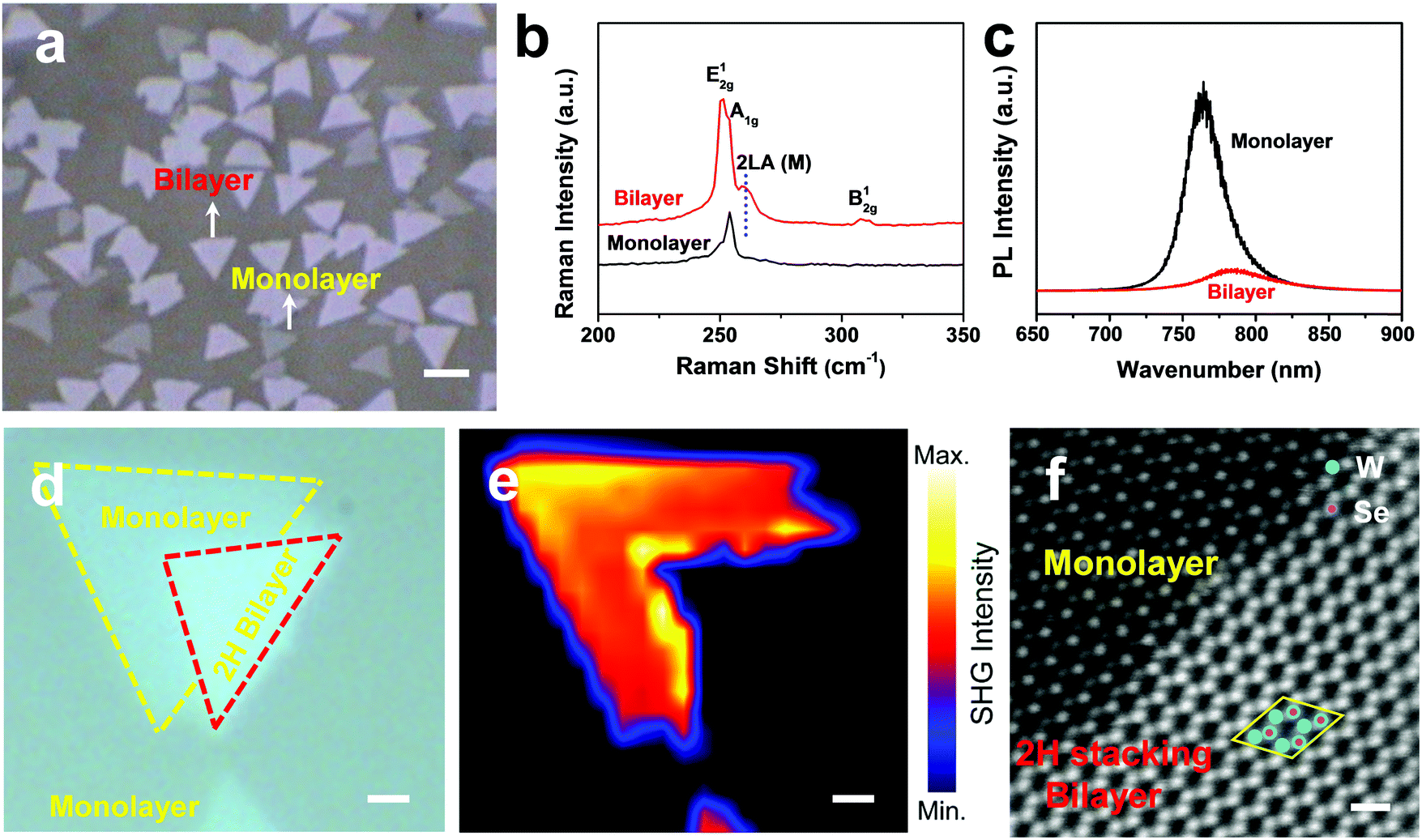 | ||
| Fig. 1 (a) Optical micrograph of monolayer/bilayer WSe2 crystals as-grown on a c-plane sapphire substrate. The amount of WO3 is 0.3 g, while the amount of Se powder is 5.0 g. A high purity of H2/Ar is the carrier gas with a fixed flow rate of 5/65 sccm/sccm. The TSe and TWO3 are maintained at 250 °C and 895 °C, respectively. The growth pressure of the furnace is 10 Torr for the whole CVD growth and the growth time is 15 min; (b) the Raman spectra measurements for monolayer (black) and bilayer (red) WSe2 crystals; (c) the PL spectra measurements for monolayer (black) and bilayer (red) WSe2 crystals; (d) optical micrograph of a bilayer WSe2 crystal with a monolayer WSe2 crystal as a reference; (e) the corresponding SHG intensity mapping obtained by pixel-to-pixel spatial scanning on the crystals in (d); (f) the HAADF-STEM image for the 2H stacking bilayer WSe2 crystal (selected from (a)). Scale bars: a, 30 μm; d, 2 μm; e, 2 μm; f, 0.5 nm. | ||
When the amount of Se is ≤3 g, scattered WO3−x nanowires or particles are formed (Fig. S2a–c, ESI†). It's been experimentally demonstrated that, for small amounts of Se, almost no WSe2 ultrathin crystals are formed from the WO3−x nanowires/particles because of the extremely inadequate selenization. On increasing the level of Se loading, the selenization becomes sufficient, and more and more WO3−x is converted into WSe2.38,39 When the amount of Se reaches 4 g, the WSe2 domains are mainly monolayers. When the amount of Se is around 5 g, under the action of a suitable amount of second layer nucleation on the first WSe2 layer, they continue to grow and cover the first monolayers to form bilayer WSe2 crystals (layer-by-layer growth). Meanwhile, the WSe2 domains are scattered across the sapphire substrate with low nucleation density which can permit the large crystal domain size (few tens of micron), as shown in Fig. S2e and f (ESI†).25,26 When the amount of Se is >5 g, too much WSe2 nucleation will hamper the enlarging of the WSe2 monolayer and thus the bilayer dimension (flake size is smaller than 10 μm as shown in Fig. S3, ESI†). The details of the bilayer growth mechanism have been discussed hereafter in this work.
The Raman spectra E12g and photoluminescence spectroscopy (PL) of WSe2 shown in Fig. 1b and c were obtained using a 532 nm laser as the excitation wavelength. The Raman spectra exhibit the characteristic WSe2 in-plane vibrational (E12g) mode assigned at 251.1 cm−1. The most prominent resonance feature in the case of bilayer WSe2 as compared with monolayer WSe2 is the second-order Raman mode due to LA phonons at the M point in the Brillouin zone, which is labeled as 2LA(M).40,41 Moreover, the highlighted peak of B12g at ≈309 cm−1 shown in bilayer WSe2 was absent in monolayer crystals, which was consistently observed for multilayer crystals of WSe2.42,43 The PL spectra shown in Fig. 1c revealed a relatively weak PL peak for the bilayer WSe2 at 784.0 nm as compared with the monolayer WSe2. On the basis of the Raman and PL results we confirm that controlled growth of bilayer WSe2 domains was successfully performed on sapphire substrates.
SHG can serve as one reliable and nondestructive characterization method to identify the stacking orders of the atomically thin layers. As 2H stacked WSe2 possesses centrosymmetry, inducing no SHG output. Meanwhile, the monolayer WSe2 and 3R stacked WSe2 show strong SHG output due to the break of centrosymmetry.44Fig. 1d and e show the optical image and the corresponding SHG intensity mapping for a WSe2 crystal composed of both monolayer and bilayer domains. Compared to the strong SHG intensity of the monolayer WSe2, no SHG signal can be detected for the bilayer region. In addition, a sharp boundary was observed crossing the two domains, which was consistent with the bilayer profile. As a result, the monolayer WSe2 showed an obviously strong SHG response due to the lack of inversion symmetry, and meanwhile the bilayer WSe2 was endowed with a typical 2H stacking order.
We have also performed additional SHG measurements for bilayer WSe2 with diverse morphologies. As shown in Fig. S4 (ESI†), both bilayer crystals primarily exhibited 2H stacking, which has been further exemplified by the low-frequency Raman results shown in Fig. S5 (ESI†). It has been previously shown that the Raman bands in the high-frequency range are not sensitive to the change of interlayer van der Waals (vdW) interactions caused by different stacking configurations.36,45 Distinct behaviors are found in ultra-low-frequency (ULF) Raman modes, in which the two peaks for 3R(2H) stacking bilayer WSe2 belong to the in-plane shear mode (SM) and out-of-plane layer-breathing mode (LBM), respectively.36 Therefore, the peak intensity ratio between LBM and SM can be used as an index to identify the stacking order of the bilayer WSe2 complementary to SHG data. From Fig. S5 (ESI†), a clear decrease in the peak intensity of the SM from 2H to 3R stacking is observed with a corresponding increment in the LBM. Thus, the ULF Raman spectra of the various bilayer WSe2 stacking configurations are in agreement with previous reports36 and SHG data (Fig. S4, ESI†). For example, we note that the occasionally found irregular-shaped bilayer WSe2 crystal showed 2H/3R mixed stacking configurations (Fig. S5b, ESI†), which is consistent with their corresponding SHG results shown in Fig. S4a (ESI†). Additionally, the stacking configurations can be studied with atomic precision using aberration-corrected STEM. The low-magnification HAADF-STEM image of the top-view bilayer WSe2 sample and corresponding elemental mapping images are shown in Fig. S6 (ESI†). In the Z-contrast high-angle-annular dark-field STEM imaging shown in Fig. 1f, the intensity strongly depends on the atomic weight and the number of monolayers. The high intensity sites correspond to the heavy atoms (i.e. W) or thicker sample, showing a contrast difference with the lighter Se atom. The STEM image clearly shows the arrangements of 2H stacked bilayer WSe2,36 corroborating the concluded results from SHG and low-frequency Raman.
In this work, we used as-supplied sapphire substrates to grow WSe2 bilayer crystals for the investigation of the growth mechanism. For the CVD parameters grown on this type of substrate, both monolayer and bilayer WSe2 crystals are inclined to be formed at random orientations, as shown in Fig. 1a. AFM measurements were further performed to study the growth mechanism of bilayer WSe2 crystals. A few selected flakes yet to complete the bilayer growth were examined to explore the details. In Fig. 2a, the corresponding inset height profile yields the thickness of the WSe2 crystal of ≈0.8 nm, in agreement with the previously reported thickness of monolayer WSe2 crystals.3 The small particles were the multilayer seeds occasionally observed in monolayer crystals.46 From the zoomed-in image as shown in Fig. 2b, it's been found that the bilayer nuclei initially grow from the sapphire atomic steps (so-called “step direction”). This phenomenon was further demonstrated by a monolayer WSe2 grain boundary crystal with bilayer nuclei on top, as shown in Fig. S7a and b (ESI†). The bilayer nuclei can be clearly seen initially growing along the sapphire atomic steps. These results provide a powerful argument with the fact that the bilayer nuclei growth originates from the atomic steps.
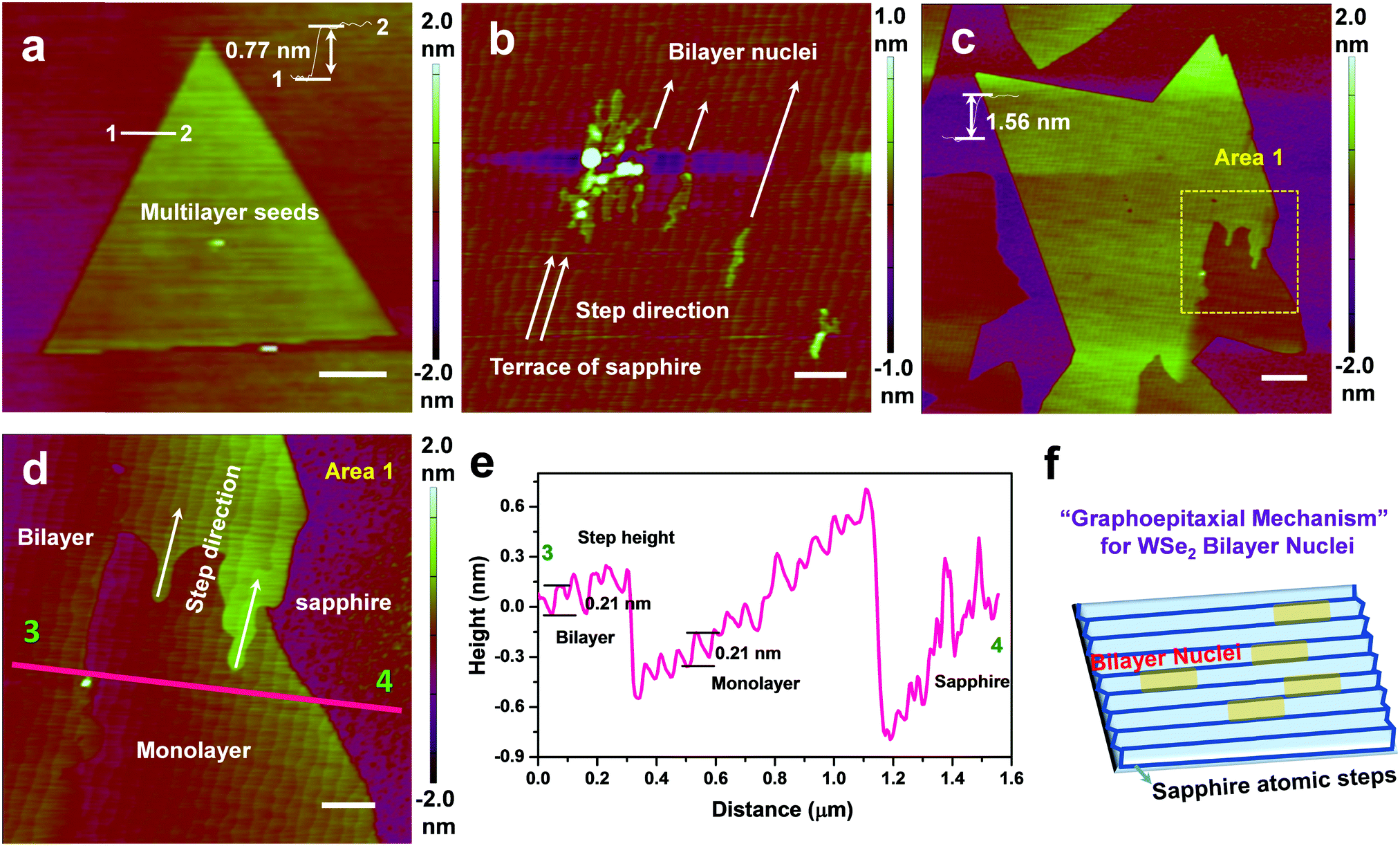 | ||
| Fig. 2 (a and b) AFM topographic images of a monolayer WSe2 crystal with bilayer nuclei in the center area. The inset height profile was ∼0.8 nm, indicating a monolayer thickness of WSe2. The zoomed-in AFM image in b shows initial WSe2 bilayer nuclei aligned growth on the atomic steps of sapphire. (c and d) AFM topographic images of bilayer WSe2 crystals. The inset height profile in c was ∼1.6 nm, indicating a bilayer thickness of WSe2. (e) The vertical profile was taken along the magenta line indicated in d (from 3 to 4). The average step height of sapphire terrace with monolayer/bilayer WSe2 covering was ∼0.2 nm. The small corrugation on the bare sapphire surface was 0.2–0.5 nm. (f) The proposed schematic of WSe2 bilayer nuclei growth along the surface step nanogrooves of sapphire. The bilayer nuclei alignments on the atomic steps abide by the graphoepitaxial mechanism. Scale bars: a, 2 μm; b, 200 nm; c, 500 nm; d, 200 nm. | ||
To better understand the influence of the atomic steps on the aligned growth of bilayer WSe2 nuclei, we compared the step height and roughness of the area with and without being covered by WSe2 monolayer and bilayer. Fig. 2c and d show representative AFM topographic images of the bilayer WSe2 crystal. Interestingly, the corrugation features are evident from the bare sapphire surface shown in Fig. 2d and the corresponding height profile in Fig. 2e (right part; corrugations of 0.2 to 0.5 nm). In contrast, the pronounced atomic steps with a periodically distributed pattern can be seen on the location covered with monolayer as well as bilayer WSe2 crystals. The periodicity and oscillation of the step heights also appear to be more regular than for the bare sapphire. These drastic atomic step heights are thought to be formed through strong interactions between WSe2 and the sapphire terrace. The most striking observation was that the average atomic step height was ∼0.21 nm for the sapphire with the WSe2 grown on top. The height was similar to the step height measured on as-supplied sapphire after high temperature annealing (Fig. S8, ESI†) and the reported literature.22,29,30
Since the bilayer WSe2 nuclei growth appears to be mediated by the atomic steps on sapphire's surface, we hypothesized that the bilayer WSe2 nuclei alignment on the atomic steps could resemble the graphoepitaxy effect (see Fig. 2f). Such phenomenon is known to affect the crystallographic orientation of the overlayer in artificial surface-relief structures.33,47,48 Two main factors are proposed to be involved in the graphoepitaxy mechanism of bilayer nuclei aligned growth: Firstly, we find that the atomic steps with the WSe2 layer atop have become more vivid (see relevant AFM analysis) as compared with the bare sapphire, which is similar to the phenomena obtained by different artificial means,47,48 and high-temperature annealing.22,29,30,49 Secondly, the pronounced atomic steps could enhance the seeding of the bilayer nuclei owing to energy lowering and thus lead to the bilayer nuclei growth orientation following the step direction.
In addition, once the monolayer/bilayer WSe2 nucleates on the sapphire, the surface adsorbates were driven out and the surface roughness reduces (Fig. S9 and Table S1, ESI†). We attribute this to the fact that the irregularly small corrugations seen on the bare sapphire are glossed over by the WSe2 crystals, i.e. being smoothened out. A similar reduction in surface roughness is observed on the bare sapphire surface upon annealing at high temperatures (see Table S1, ESI†). Hence, the pronounced atomic step heights and the ultrasmooth surface induced by the WSe2 crystal atop are proposed as the main reasons for the bilayer nuclei initially growing on the atomic steps of sapphire. Moreover, the same growth mode also applies to the 3rd layer WSe2. Fig. 3a and b illustrate the typical bilayer WSe2 with the 3rd layer WSe2 nuclei growing along the atomic steps of sapphires. The Raman spectra for the trilayer WSe2 are shown in Fig. S10 (ESI†). Fig. S11 (ESI†) shows more examples validating the bilayer nuclei growth behaviors. Taking the bilayer WSe2 growth as an example, we illustrate in Fig. 3e with schematics how the bilayer WSe2 nuclei nucleate along the enhanced atomic steps (yellow solid lines) and eventually become a superimposed bilayer crystal, following a layer-by-layer (LBL) growth mode.50,51 Although the growth orientation of the upper layer nuclei was guided by the sapphire substrate steps, the stacking configuration of the upper layer seems irrelevant to the underlying sapphire crystal orientation. The first layer WSe2 are not oriented in the same direction but the upper layers could still recognize the crystal lattice of the first layer WSe2 to form 2H stacking configurations, suggesting that the second layer crystal stacking is governed by the vdW epitaxial processes on the first layer of WSe2.
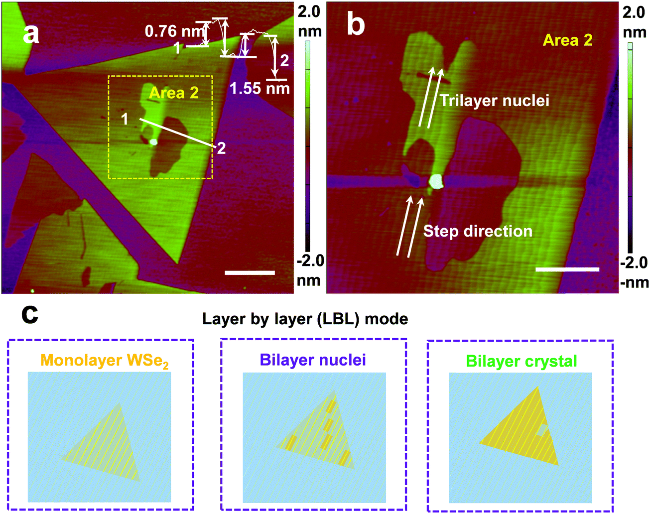 | ||
| Fig. 3 (a) AFM topographic images of a bilayer WSe2 crystal with the 3rd layer nuclei. The inset height profile demonstrated a bilayer thickness of WSe2 and trilayer nuclei formed on the topmost surface. (b) The zoomed-in AFM image in a showed WSe2 bilayer and trilayer nuclei growth guided by the atomic steps. (c) Schematics of the layer-by-layer growth mode in this work. The yellow dashed lines are the atomic steps of the bare sapphire and the yellow solid lines are the atomic steps of sapphire with WSe2 crystals atop. Scale bars: a, 1 μm; b, 500 nm. | ||
Charge transport measurements were performed to evaluate the electronic property of our bilayer WSe2 crystals as-grown on sapphire substrates. Standard electron beam lithography was used to fabricate side-gate bilayer WSe2 field-effect transistors directly on sapphire substrates. Device structure and a representative optical image of the device are shown in Fig. 4a, where Pd (20 nm)/Au (70 nm) was used as the contact metal and an ionic liquid (Cg = 5.0 μF cm−2) was dropped across the channel as the top gate dielectric material. The Raman and PL of the WSe2 samples before and after fabrication are shown in Fig. S12 (ESI†) to confirm the quality of the samples. Unfortunately, the quality of the WSe2 samples appears to be compromised after device fabrication probably due to PMMA contamination during the EBL process. Device characterization was carried out in a vacuum chamber at room temperature to exclude unwanted doping effects due to H2O or O2 present in ambient air. The voltage applied between the source and drain electrodes (VD) was varied from −2 to 2 V for both monolayer and bilayer crystal-based devices, as shown in Fig. S13a and b (ESI†), indicating the good contact of the metal with the WSe2 channel. Both devices exhibit predominantly p-channel characteristics in accordance with previously published results, but with evidence of pronounced electron transport under positive VG. Interestingly, monolayer WSe2-based transistors appear to be more ambipolar than bilayer WSe2 devices. The hole mobility extracted from the transfer characteristics in Fig. 4b were ≈11 cm2 V−1 s−1 and ≈40 cm2 V−1 s−1 for monolayer and bilayer WSe2 crystals, respectively. Moreover, the subthreshold slopes (SS) for monolayer and bilayer WSe2 transistors were 229 mV dec−1 and 201 mV dec−1, respectively, as shown in Fig. S13c (ESI†). The similarity in the derived SS values indicates good gate control over the p-channel for both monolayer and bilayer WSe2 FETs.
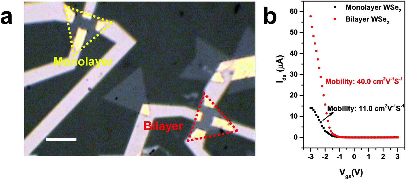 | ||
| Fig. 4 (a) Optical image of monolayer/bilayer WSe2 crystals for the device fabrication. Scale bar: 15 μm; (b) Ids as a function of Vgs for monolayer/bilayer WSe2 crystals device. Vd = 0.5 V, Cg = 5.0 μF cm−2. The mobility of monolayer and bilayer crystals were measured to be 11.0 and 40.0 cm2 V−1 s−1, respectively. | ||
It has been reported that the hole mobility in monolayer and multilayer TMD devices is affected by intrinsic phonon scattering within the channel as well as extrinsic scattering phenomena originating from charged impurities at the channel/dielectric interface, charge trapping states, substrate surface roughness and remote surface optical phonons.52–54 In particular, coulomb scattering from charged impurities at the channel/substrate interface has been proposed as the primary reason for the lower room-temperature mobility in TMDs.52–54 Meanwhile, the intrinsic mobility of bilayer TMD is also predicted to be higher than monolayer TMD.55 Overall, the field-effect measurements suggest that our CVD bilayer WSe2 crystals are of good quality and thus hold promising prospects toward applications in nanoelectronic devices.
Conclusions
In conclusion, we have demonstrated controlled growth of 2H stacked bilayer WSe2 on c-plane sapphire substrates by the CVD method. The pure 2H stacking configuration of bilayer WSe2 was confirmed by collective characterization techniques including SHG, low-frequency Raman and STEM measurements. We demonstrate the nuclei growth of bilayer WSe2 sliding along the pronounced atomic steps induced by WSe2 crystals atop, resembling the graphoepitaxy mechanism. And the alignment growth of bilayer nuclei on atomic steps gives rise to the gradual formation of overlapped bilayer crystals, abiding by the LBL growth mode. Importantly, the bilayers in our growth conditions lead to the most thermodynamically stable 2H stacked bilayer WSe2 through vdW epitaxial growth, exhibiting substantially enhanced hole mobility, three times higher than that of monolayer WSe2. The discovery of atomic steps guiding bilayer nuclei growth revealed in this work provides new insights into the growth, which could be applicable to other TMD systems, hence paving the way towards controllable large-area growth of bilayer and multilayer TMDs crystals for electronic and optoelectronic applications.Methods
Material synthesis
The monolayer/bilayer WSe2 crystals were grown by the chemical vapor deposition (CVD) method. Typically, WO3 powder (300 mg, Sigma-Aldrich, 99.9%) was placed into a quartz boat in a high temperature furnace, while the Se powder (Sigma-Aldrich, 99.99%) was placed into a separate low temperature furnace upstream of WO3. The carrier gas of H2 and Ar allows the diffusion of Se vapor into the reaction area. During the heating stage, H2 firstly reacts with WO3 to form WO3−x (x = 0–3) suboxides. With regard to the WSe2 growth stage, all WSe2 formation reactions were equally given 15 min growth time starting at 0 min when the temperature of the WO3 furnace reached 890–900 °C. The Se powder in the low temperature zone was heated to 250–260 °C and carried downstream using the carrier gas to the reaction area at times of 3 min before the WO3 precursors reached the required temperature. The c-plane sapphire substrates were put downstream of the WO3 boat, where the Se and WO3 vapors were brought to the sapphire substrates by the carrier gas. The sapphire substrates are directly used without any pre-treatment. Finally, the furnace was naturally cooled down to room temperature after the temperature controller was turned off.Raman and AFM characterization
The as-grown WSe2 crystals are characterized using optical microscopy (Witec alpha 300 confocal Raman microscope) equipped with a confocal spectrometer using a 532 nm excitation laser. A typical laser spot is 1–2 μm. The thickness of the WSe2 crystals was determined by atomic force microscope (AFM, Cypher ES model from Asylum Research Oxford Instruments).SHG characterization
The SHG measurements were carried out using a Horiba Jobin–Yvon HR800 spectrometer in reflection geometry with the excitation laser perpendicular to the substrate. A mode-locked Ti/Sapphire oscillator was used as the pumping source at 800 nm wavelength (Spectra-Physics, 80 MHz, 100 fs). With a 100× objective, the pumping light was focused to a spot size of ∼2 μm in diameter on the sample. For measurement of SHG intensity mapping, the excitation laser was modulated under DuoScan mode, which is a unique hardware module to scan the laser beam on a given area using software controlled mirrors.STEM sample preparation and characterization
The WSe2 crystals were coated with polymethylmethacrylate (PMMA) to support the film during the transfer process. To separate the film from the sapphire substrate, the samples were soaked in an HF solution (HF![[thin space (1/6-em)]](https://www.rsc.org/images/entities/char_2009.gif) :H2O = 1:1) for 15 min. After rinsing with deionized water several times, the samples were dipped into water and the film was released from the substrate by tweezers. With the film floating on the water surface, we used a QUANTIFOIL holey carbon film on a 400 Mesh Nickel TEM grid (Agar Scientific) to scoop the film. The PMMA was then removed by acetone for more than 1 h. The TEM grid with WSe2 crystals was finally baked in a vacuum (<10−6 Torr) at 350 °C overnight to remove the PMMA residue. HAADF-STEM imaging was conducted at 80 kV using a ThermoFisher USA (former FEI Co) Titan Themis Z (40–300 kV) TEM equipped with a double Cs (spherical aberration) corrector, a high brightness electron gun (x-FEG) and a Fischione STEM detector.
:H2O = 1:1) for 15 min. After rinsing with deionized water several times, the samples were dipped into water and the film was released from the substrate by tweezers. With the film floating on the water surface, we used a QUANTIFOIL holey carbon film on a 400 Mesh Nickel TEM grid (Agar Scientific) to scoop the film. The PMMA was then removed by acetone for more than 1 h. The TEM grid with WSe2 crystals was finally baked in a vacuum (<10−6 Torr) at 350 °C overnight to remove the PMMA residue. HAADF-STEM imaging was conducted at 80 kV using a ThermoFisher USA (former FEI Co) Titan Themis Z (40–300 kV) TEM equipped with a double Cs (spherical aberration) corrector, a high brightness electron gun (x-FEG) and a Fischione STEM detector.
Device fabrication and transport measurement
FETs were fabricated on WSe2 monolayer and bilayer crystals directly on sapphire substrates under the same conditions. The devices were fabricated by the standard E-beam lithography (EBL) process using a PMMA 950 A4 photoresist. Before the exposure, a thick sputtered Au film (6 nm in thickness) was coated on the photoresist to avoid the severe charging effect on the sapphire surface. The first EBL process was to make the alignment markers on the sapphire surface and the second process was to pattern the source-drain and gate electrodes, followed by e-beam evaporation of Pd (20 nm)/Au (70 nm) and a standard lift-off process by acetone. The FET transfer characteristics were measured under vacuum by a Keithley 4200 semiconductor parameter analyzer (Vd = 0.5 V). The ionic liquid (Cg = 5.0 μF cm−2) was used to gate WSe2 and the p-type semiconductor behavior.Author contributions
The manuscript was written through contributions of all authors. All authors have given approval to the final version of the manuscript.Conflicts of interest
There are no conflicts to declare.Acknowledgements
T. D. A., V. T., X. Z., and L. L. acknowledge the support from King Abdullah University of Science and Technology. V. T. acknowledges the support from User Proposals (#4420 and #5067) at the Molecular Foundry, Lawrence Berkeley National Lab, supported by the Office of Basic Energy Sciences, of the U.S. Department of Energy under Contract No. DE-AC02-05CH11231. We would also like to acknowledge the support from Core Lab in KAUST.References
- M.-Y. Li, S.-K. Su, H.-S. P. Wong and L.-J. Li, How 2D semiconductors could extend Moore's law, Nature, 2019, 567, 169 CrossRef CAS PubMed.
- C. Huang, S. Wu, A. M. Sanchez, J. J. P. Peters, R. Beanland, J. S. Ross, P. Rivera, W. Yao, D. H. Cobden and X. Xu, Lateral heterojunctions within monolayer MoSe2–WSe2 semiconductors, Nat. Mater., 2014, 13, 1096 CrossRef CAS PubMed.
- M.-Y. Li, Y. Shi, C.-C. Cheng, L.-S. Lu, Y.-C. Lin, H.-L. Tang, M.-L. Tsai, C.-W. Chu, K.-H. Wei, J.-H. He, W.-H. Chang, K. Suenaga and L.-J. Li, Epitaxial growth of a monolayer WSe2-MoS2 lateral p-n junction with an atomically sharp interface, Science, 2015, 349(6247), 524–528 CrossRef CAS PubMed.
- A.-Y. Lu, H. Zhu, J. Xiao, C.-P. Chuu, Y. Han, M.-H. Chiu, C.-C. Cheng, C.-W. Yang, K.-H. Wei, Y. Yang, Y. Wang, D. Sokaras, D. Nordlund, P. Yang, D. A. Muller, M.-Y. Chou, X. Zhang and L.-J. Li, Janus monolayers of transition metal dichalcogenides, Nat. Nanotechnol., 2017, 12, 744 CrossRef CAS PubMed.
- A. Pospischil, M. M. Furchi and T. Mueller, Solar-energy conversion and light emission in an atomic monolayer p–n diode, Nat. Nanotechnol., 2014, 9, 257 CrossRef CAS PubMed.
- Q. H. Wang, K. Kalantar-Zadeh, A. Kis, J. N. Coleman and M. S. Strano, Electronics and optoelectronics of two-dimensional transition metal dichalcogenides, Nat. Nanotechnol., 2012, 7, 699 CrossRef CAS PubMed.
- C.-H. Lee, G.-H. Lee, A. M. van der Zande, W. Chen, Y. Li, M. Han, X. Cui, G. Arefe, C. Nuckolls, T. F. Heinz, J. Guo, J. Hone and P. Kim, Atomically thin p–n junctions with van der Waals heterointerfaces, Nat. Nanotechnol., 2014, 9, 676 CrossRef CAS PubMed.
- V. Nicolosi, M. Chhowalla, M. G. Kanatzidis, M. S. Strano and J. N. Coleman, Liquid Exfoliation of Layered, Mater. Sci., 2013, 340, 6139 Search PubMed.
- J. Zhou, J. Lin, X. Huang, Y. Zhou, Y. Chen, J. Xia, H. Wang, Y. Xie, H. Yu, J. Lei, D. Wu, F. Liu, Q. Fu, Q. Zeng, C.-H. Hsu, C. Yang, L. Lu, T. Yu, Z. Shen, H. Lin, B. I. Yakobson, Q. Liu, K. Suenaga, G. Liu and Z. Liu, A library of atomically thin metal chalcogenides, Nature, 2018, 556(7701), 355–359 CrossRef CAS PubMed.
- Q. Feng, N. Mao, J. Wu, H. Xu, C. Wang, J. Zhang and L. Xie, Growth of MoS2(1−x)Se2x(x = 0.41–1.00) Monolayer Alloys with Controlled Morphology by Physical Vapor Deposition, ACS Nano, 2015, 9(7), 7450–7455 CrossRef CAS PubMed.
- C. Gong, C. Huang, J. Miller, L. Cheng, Y. Hao, D. Cobden, J. Kim, R. S. Ruoff, R. M. Wallace, K. Cho, X. Xu and Y. J. Chabal, Metal Contacts on Physical Vapor Deposited Monolayer MoS2, ACS Nano, 2013, 7(12), 11350–11357 CrossRef CAS PubMed.
- J.-H. Huang, K.-Y. Deng, P.-S. Liu, C.-T. Wu, C.-T. Chou, W.-H. Chang, Y.-J. Lee and T.-H. Hou, Large-Area 2D Layered MoTe2 by Physical Vapor Deposition and Solid-Phase Crystallization in a Tellurium-Free Atmosphere, Adv. Mater. Interfaces, 2017, 4(17), 1700157 CrossRef.
- H. J. Liu, L. Jiao, L. Xie, F. Yang, J. L. Chen, W. K. Ho, C. L. Gao, J. F. Jia, X. D. Cui and M. H. Xie, Molecular-beam epitaxy of monolayer and bilayer WSe2: a scanning tunneling microscopy/spectroscopy study and deduction of exciton binding energy, 2D Mater., 2015, 2(3), 034004 CrossRef.
- A. Roy, H. C. P. Movva, B. Satpati, K. Kim, R. Dey, A. Rai, T. Pramanik, S. Guchhait, E. Tutuc and S. K. Banerjee, Structural and Electrical Properties of MoTe2 and MoSe2 Grown by Molecular Beam Epitaxy, ACS Appl. Mater. Interfaces, 2016, 8(11), 7396–7402 CrossRef CAS PubMed.
- K. F. Mak, K. He, J. Shan and T. F. Heinz, Control of valley polarization in monolayer MoS2 by optical helicity, Nat. Nanotechnol., 2012, 7, 494 CrossRef CAS PubMed.
- H. Zeng, J. Dai, W. Yao, D. Xiao and X. Cui, Valley polarization in MoS2 monolayers by optical pumping, Nat. Nanotechnol., 2012, 7, 490 CrossRef CAS PubMed.
- F. Withers, O. Del Pozo-Zamudio, A. Mishchenko, A. P. Rooney, A. Gholinia, K. Watanabe, T. Taniguchi, S. J. Haigh, A. K. Geim, A. I. Tartakovskii and K. S. Novoselov, Light-emitting diodes by band-structure engineering in van der Waals heterostructures, Nat. Mater., 2015, 14, 301 CrossRef CAS PubMed.
- K. F. Mak and J. Shan, Photonics and optoelectronics of 2D semiconductor transition metal dichalcogenides, Nat. Photonics, 2016, 10, 216 CrossRef CAS.
- J. R. Schaibley, H. Yu, G. Clark, P. Rivera, J. S. Ross, K. L. Seyler, W. Yao and X. Xu, Valleytronics in 2D materials, Nat. Rev. Mater., 2016, 1, 16055 CrossRef CAS.
- J. Chen, B. Liu, Y. Liu, W. Tang, C. T. Nai, L. Li, J. Zheng, L. Gao, Y. Zheng, H. S. Shin, H. Y. Jeong and K. P. Loh, Chemical Vapor Deposition of Large-Sized Hexagonal WSe2 Crystals on Dielectric Substrates, Adv. Mater., 2015, 27(42), 6722–6727 CrossRef CAS PubMed.
- L. Chen, B. Liu, A. N. Abbas, Y. Ma, X. Fang, Y. Liu and C. Zhou, Screw-Dislocation-Driven Growth of Two-Dimensional Few-Layer and Pyramid-like WSe2 by Sulfur-Assisted Chemical Vapor Deposition, ACS Nano, 2014, 8(11), 11543–11551 CrossRef CAS PubMed.
- L. Chen, B. Liu, M. Ge, Y. Ma, A. N. Abbas and C. Zhou, Step-Edge-Guided Nucleation and Growth of Aligned WSe2 on Sapphire via a Layer-over-Layer Growth Mode, ACS Nano, 2015, 9(8), 8368–8375 CrossRef CAS PubMed.
- J. Liu, M. Zeng, L. Wang, Y. Chen, Z. Xing, T. Zhang, Z. Liu, J. Zuo, F. Nan, R. G. Mendes, S. Chen, F. Ren, Q. Wang, M. H. Rümmeli and L. Fu, Ultrafast Self-Limited Growth of Strictly Monolayer WSe2 Crystals, Small, 2016, 12(41), 5741–5749 CrossRef CAS PubMed.
- M. Xia, B. Li, K. Yin, G. Capellini, G. Niu, Y. Gong, W. Zhou, P. M. Ajayan and Y.-H. Xie, Spectroscopic Signatures of AA′ and AB Stacking of Chemical Vapor Deposited Bilayer MoS2, ACS Nano, 2015, 9(12), 12246–12254 CrossRef CAS PubMed.
- A. Zobel, A. Boson, P. M. Wilson, D. S. Muratov, D. V. Kuznetsov and A. Sinitskii, Chemical vapour deposition and characterization of uniform bilayer and trilayer MoS2 crystals, J. Mater. Chem. C, 2016, 4(47), 11081–11087 RSC.
- S. Yang, J. Kang, Q. Yue and K. Yao, Vapor Phase Growth and Imaging Stacking Order of Bilayer Molybdenum Disulfide, J. Phys. Chem. C, 2014, 118(17), 9203–9208 CrossRef CAS.
- H. Ye, J. Zhou, D. Er, C. C. Price, Z. Yu, Y. Liu, J. Lowengrub, J. Lou, Z. Liu and V. B. Shenoy, Toward a Mechanistic Understanding of Vertical Growth of van der Waals Stacked 2D Materials: A Multiscale Model and Experiments, ACS Nano, 2017, 11(12), 12780–12788 CrossRef CAS PubMed.
- S. Ghatak, A. N. Pal and A. Ghosh, Nature of Electronic States in Atomically Thin MoS2 Field-Effect Transistors, ACS Nano, 2011, 5(10), 7707–7712 CrossRef CAS PubMed.
- M. Yoshimoto, T. Maeda, T. Ohnishi, H. Koinuma, O. Ishiyama, M. Shinohara, M. Kubo, R. Miura and A. Miyamoto, Atomic-scale formation of ultrasmooth surfaces on sapphire substrates for high-quality thin-film fabrication, Appl. Phys. Lett., 1995, 67(18), 2615–2617 CrossRef CAS.
- D. Dumcenco, D. Ovchinnikov, K. Marinov, P. Lazić, M. Gibertini, N. Marzari, O. L. Sanchez, Y.-C. Kung, D. Krasnozhon, M.-W. Chen, S. Bertolazzi, P. Gillet, A. Fontcuberta i Morral, A. Radenovic and A. Kis, Large-Area Epitaxial Monolayer MoS2, ACS Nano, 2015, 9(4), 4611–4620 CrossRef CAS PubMed.
- S. Han, X. Liu and C. Zhou, Template-Free Directional Growth of Single-Walled Carbon Nanotubes on a- and r-Plane Sapphire, J. Am. Chem. Soc., 2005, 127(15), 5294–5295 CrossRef CAS PubMed.
- A. Ismach, L. Segev, E. Wachtel and E. Joselevich, Atomic-Step-Templated Formation of Single Wall Carbon Nanotube Patterns, Angew. Chem., Int. Ed., 2004, 43(45), 6140–6143 CrossRef CAS PubMed.
- D. Tsivion, M. Schvartzman, R. Popovitz-Biro, P. von Huth and E. Joselevich, Guided Growth of Millimeter-Long Horizontal Nanowires with Controlled Orientations, Science, 2011, 333(6045), 1003–1007 CrossRef CAS PubMed.
- S. Saadi, F. Abild-Pedersen, S. Helveg, J. Sehested, B. Hinnemann, C. C. Appel and J. K. Nørskov, On the Role of Metal Step-Edges in Graphene Growth, J. Phys. Chem. C, 2010, 114(25), 11221–11227 CrossRef CAS.
- S. Curiotto and D. Chatain, Surface composition and morphology of c-, and m-sapphire surfaces in O2 and H2 environments, Surf. Sci., 2009, 603(17), 2688–2697 CrossRef CAS.
- A. A. Puretzky, L. Liang, X. Li, K. Xiao, K. Wang, M. Mahjouri-Samani, L. Basile, J. C. Idrobo, B. G. Sumpter, V. Meunier and D. B. Geohegan, Low-Frequency Raman Fingerprints of Two-Dimensional Metal Dichalcogenide Layer Stacking Configurations, ACS Nano, 2015, 9(6), 6333–6342 CrossRef CAS PubMed.
- J. He, K. Hummer and C. Franchini, Stacking effects on the electronic and optical properties of bilayer transition metal dichalcogenides, Phys. Rev. B: Condens. Matter Mater. Phys., 2014, 89(7), 075409 CrossRef.
- J.-K. Huang, J. Pu, C.-L. Hsu, M.-H. Chiu, Z.-Y. Juang, Y.-H. Chang, W.-H. Chang, Y. Iwasa, T. Takenobu and L.-J. Li, Large-Area Synthesis of Highly Crystalline WSe2 Monolayers and Device Applications, ACS Nano, 2014, 8(1), 923–930 CrossRef CAS PubMed.
- H. Kim, S. J. Yun, J. C. Park, M. H. Park, J.-H. Park, K. K. Kim and Y. H. Lee, Seed Growth of Tungsten Diselenide Nanotubes from Tungsten Oxides, Small, 2015, 11(18), 2192–2199 CrossRef CAS PubMed.
- A. Molina-Sánchez and L. Wirtz, Phonons in single-layer and few-layer MoS2 and WS2, Phys. Rev. B: Condens. Matter Mater. Phys., 2011, 84(15), 155413 CrossRef.
- C. Sourisseau, F. Cruege, M. Fouassier and M. Alba, Second-order Raman effects, inelastic neutron scattering and lattice dynamics in 2H-WS2, Chem. Phys., 1991, 150(2), 281–293 CrossRef CAS.
- W. Zhao, Z. Ghorannevis, K. K. Amara, J. R. Pang, M. Toh, X. Zhang, C. Kloc, P. H. Tan and G. Eda, Lattice dynamics in mono- and few-layer sheets of WS2 and WSe2, Nanoscale, 2013, 5(20), 9677–9683 RSC.
- Y. Zhao, X. Luo, H. Li, J. Zhang, P. T. Araujo, C. K. Gan, J. Wu, H. Zhang, S. Y. Quek, M. S. Dresselhaus and Q. Xiong, Interlayer Breathing and Shear Modes in Few-Trilayer MoS2 and WSe2, Nano Lett., 2013, 13(3), 1007–1015 CrossRef CAS PubMed.
- W.-T. Hsu, Z.-A. Zhao, L.-J. Li, C.-H. Chen, M.-H. Chiu, P.-S. Chang, Y.-C. Chou and W.-H. Chang, Second Harmonic Generation from Artificially Stacked Transition Metal Dichalcogenide Twisted Bilayers, ACS Nano, 2014, 8(3), 2951–2958 CrossRef CAS PubMed.
- J. Xia, J. Yan and Z. X. Shen, Transition metal dichalcogenides: structural, optical and electronic property tuning via thickness and stacking, FlatChem, 2017, 4, 1–19 CrossRef CAS.
- A. Aljarb, Z. Cao, H.-L. Tang, J.-K. Huang, M. Li, W. Hu, L. Cavallo and L.-J. Li, Substrate Lattice-Guided Seed Formation Controls the Orientation of 2D Transition-Metal Dichalcogenides, ACS Nano, 2017, 11(9), 9215–9222 CrossRef CAS PubMed.
- M. W. Geis, D. C. Flanders and H. I. Smith, Crystallographic orientation of silicon on an amorphous substrate using an artificial surface-relief grating and laser crystallization, Appl. Phys. Lett., 1979, 35(1), 71–74 CrossRef CAS.
- M. W. Geis, B. Y. Tsaur and D. C. Flanders, Graphoepitaxy of germanium on gratings with square-wave and sawtooth profiles, Appl. Phys. Lett., 1982, 41(6), 526–529 CrossRef CAS.
- C. Barth and M. Reichling, Imaging the atomic arrangements on the high-temperature reconstructed α-Al2O3(0001) surface, Nature, 2001, 414, 54 CrossRef CAS PubMed.
- M. Kawasaki, K. Takahashi, T. Maeda, R. Tsuchiya, M. Shinohara, O. Ishiyama, T. Yonezawa, M. Yoshimoto and H. Koinuma, Atomic Control of the SrTiO3 Crystal, Surf. Sci., 1994, 266(5190), 1540–1542 CAS.
- K. Yan, H. Peng, Y. Zhou, H. Li and Z. Liu, Formation of Bilayer Bernal Graphene: Layer-by-Layer Epitaxy via Chemical Vapor Deposition, Nano Lett., 2011, 11(3), 1106–1110 CrossRef CAS PubMed.
- B. Radisavljevic and A. Kis, Mobility engineering and a metal–insulator transition in monolayer MoS2, Nat. Mater., 2013, 12, 815 CrossRef CAS PubMed.
- K. Kaasbjerg, K. S. Thygesen and K. W. Jacobsen, Phonon-limited mobility in n-type single-layer MoS2 from first principles, Phys. Rev. B: Condens. Matter Mater. Phys., 2012, 85(11), 115317 CrossRef.
- W. Liu, J. Kang, D. Sarkar, Y. Khatami, D. Jena and K. Banerjee, Role of Metal Contacts in Designing High-Performance Monolayer n-Type WSe2 Field Effect Transistors, Nano Lett., 2013, 13(5), 1983–1990 CrossRef CAS PubMed.
- B. W. H. Baugher, H. O. H. Churchill, Y. Yang and P. Jarillo-Herrero, Intrinsic Electronic Transport Properties of High-Quality Monolayer and Bilayer MoS2, Nano Lett., 2013, 13(9), 4212–4216 CrossRef CAS PubMed.
Footnote |
| † Electronic supplementary information (ESI) available. See DOI: 10.1039/c9nh00260j |
| This journal is © The Royal Society of Chemistry 2019 |