
Nanomechanics of low-dimensional materials for functional applications
Sufeng
Fan†
 a,
Xiaobin
Feng†
a,
Ying
Han†
a,
Zhengjie
Fan
ab and
Yang
Lu
*acd
a,
Xiaobin
Feng†
a,
Ying
Han†
a,
Zhengjie
Fan
ab and
Yang
Lu
*acd
aDepartment of Mechanical Engineering, City University of Hong Kong, Kowloon, Hong Kong. E-mail: yanglu@cityu.edu.hk
bState Key Laboratory for Manufacturing Systems Engineering, Xi’an Jiaotong University, 710049, Xi'an, China
cDepartment of Materials Science and Engineering, City University of Hong Kong, Kowloon, Hong Kong
dCityU-Xidian Joint Laboratory of Micro/Nano-Manufacturing, Shenzhen 518057, China
First published on 26th April 2019
Abstract
When materials’ characteristic dimensions are reduced to the nanoscale regime, their mechanical properties will vary significantly to that of their bulk counterparts. Recently low-dimensional materials, including one-dimensional (1D) and two-dimensional (2D) nanomaterials, have attracted the widespread attention of academia and industry because of their unique (e.g., thermal, optical, electrical, catalytic) properties. These outstanding properties give them a wide variety of functional applications; however, reliable devices and practical applications call for high structural reliability and mechanical robustness of these nanoscale building blocks. Therefore, there is a need to investigate and characterize the nanomechanical properties and deformation mechanisms of low-dimensional materials but this remains highly challenging. In this Focus article, we summarize the recent progress made in the nanomechanical studies on some representative 1D/2D crystalline nanomaterials, with a special emphasis on experimental research. Furthermore, the unconventional mechanical properties, such as the significantly enhanced elasticity, of these low-dimensional crystals can lead to unprecedented physical and chemical property changes, which may fundamentally change the way such materials conduct electricity/heat, transmit/emit light, and their involvement in chemical reactions. Therefore, the nanomechanical approach can be also used to tailor the materials’ functional properties and performance, by so-called strain engineering, which can open up new avenues to explore how devices can be designed and fabricated with even more dramatic changes in low-dimensional crystalline materials for information processing, communications, biomedical, and energy applications.
Introduction
With the rapid progress toward miniaturization and scalable integration in the microelectronics industry, the design and fabrication of small-scale materials with desired mechanical, electrical, thermal, and optical properties are still great challenges. Meanwhile, in the past decades, with the rapid development of nanoscience and nanotechnology, low-dimensional materials including one-dimensional (1D) nanomaterials (nanotubes, nanowires, etc.) and two-dimensional (2D) materials (graphene, layered MoS2, etc.), have become promising candidates for functional device components.1 As shown in Fig. 1, these emerging nanomaterials have become key building blocks for future nanodevices and nanomechanical and nanoelectromechanical systems (NEMS). However, compared with their fancy functional properties, their mechanical property, which is also an important factor in most practical applications, has drawn relatively less attention in nanomaterials research. Actually, many existing studies, including our recent works,2–4 have clearly shown that miniaturization can give entirely different mechanical properties to conventional crystalline materials because of the reduced size and high surface-to-volume, creating great impacts on the design, manufacturing, and service life of the relevant components, which are vital in the practical application of low-dimensional materials-based functional devices. The size-dependent mechanical and fracture behavior of crystalline materials at the nanoscale have thus generated great interest in the solid mechanics community because of their importance to the assembly, performance, and reliability of functional nanodevices and NEMS. Apart from reliable functional device applications, recent studies suggest that the nanomechanics study of low-dimensional crystalline materials could also provide a venue to manipulate and precisely tune the physical properties of the nanomaterials under applied mechanical loading, which is related to the concept of “strain engineering,” which is based on the fact that a material's physical and chemical properties are functions of the lattice parameters of the underlying crystal lattice or the elastic strain, εe, with respect to the stress-free reference state. Fundamentally, the electronic structure (band gap) changes with εe. Therefore, many physical and chemical properties can depend on the mechanical strain: thermal, magnetic, transport, and electro-optical characteristics, and the catalytic activities, which vary sensitively with εe. Moreover, unlike some other ways of changing a material's properties, such as by chemical doping, which produce a permanent, static change, mechanical straining allows the properties to be changed on the fly. So, the “strain engineering” of low-dimensional crystalline materials has become a new trend in the design and fabrication of novel nanoelectronics and optoelectronic devices.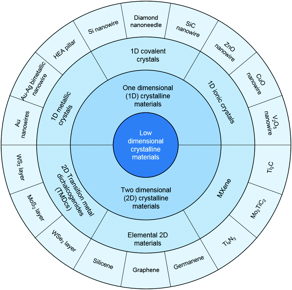 | ||
| Fig. 1 Classification and some examples of low-dimensional (1D/2D) crystalline nanomaterials. | ||
Past study of both the mechanical properties and deformation-induced physical property changes of low-dimensional crystalline materials were mostly performed using theoretical and computational methods because of the great challenges involved in experiments. Over the past two decades, due to the rapid development and advancement of nano-fabrication and characterization techniques, such as focused ion beam (FIB), in situ electron microscopy (SEM/TEM), atomic force microscopy, and nanoindentation, researchers can now perform real experiments to observe and quantify the intriguing mechanical properties, including the strength, elastic strain, and plasticity, of individual nanostructures, by using methods such as nanoindentation,5 resonance,6 uniaxial loading,2,7 bending tests,4,8,9 and fatigue tests.10,11 So this Focus article reviews the state-of-art progress in the experimental nanomechanics of 1D metallic and covalent crystalline materials as well as 2D crystals, set against the background of their functional applications. Also, the challenges that need to be solved in the near future, opportunities for nanomechanics of low-dimensional materials, and their functional device applications are also discussed herein. More importantly, we also introduce some most recent development on the “elastic strain engineering” (ESE) of low-dimensional crystalline materials, which may bring enormous new opportunities in nanomechanics research.
One-dimensional metallic crystalline materials
Metallic nanopillars, nanowires (NWs) and nanorods (NRs), with diameters ranging from a few to hundreds of nanometers, have stimulated great interest recently as important building blocks for future micro/nanoelectronics and electromechanical devices in various industrial applications. Therefore, their mechanical performance plays a key role in their reliability and other functional applications. Among various research studies, the size effect of metallic nanocrystals has received most interest in the nanomechanics community during the past decades. In the mechanical behavior of metallic materials, the size effect includes both an internal size effect and external size effect. Among these, the internal size effect is primarily related to boundaries and is depicted as the classic “Hall–Petch” relationship, with the principle being “smaller is stronger.” However, when grain sizes decrease into the nanocrystalline regime, their limited ductility/deformability becomes the Achilles’ heel of these ultrastrong nanocrystals. At the nanoscale, the sample size or the external size has an even greater effect and strongly influences the mechanical properties, and here, even nanolattices have demonstrated superior compressive specific strength and recoverability that are quite different from their bulk counterparts.12,13 Crystalline metallic pillars with diameters spanning from tens of micrometers to hundreds of nanometers demonstrated strong size effects when subjected to uniaxial compression,14,15 and it was found that dislocations would emit from the free surfaces instead of the interior when the diameter decreases to hundreds of nanometers.16 Consequently, unconventional deformation mechanisms, including dislocation starvation,17 surface dislocation self-multiplication18 and mechanical annealing,19 may occur. In this case, on the basis of the 1D metallic characteristic, some new applications arise from nano-fabrication; for instance, LIGA (a German acronym for lithographie, galvanoformung, abformung, which means lithography, electroplating, and molding) nickel with predominant mechanical performance has been used in microelectromechanical systems (MEMS) for elevated temperatures.20 Crystalline metallic NWs exhibit remarkably enhanced strengths, even ultrahigh yield strength that reaches their ideal strength, which is attributed to their reduced surface areas, dense nanotwins, uniform dislocation nucleation, and them being low or even defect free, etc.12,13,21 For characterizing such tiny specimens, advanced in situ nanomechanical measurement instruments have been developed inside SEM or TEM, such as shown in Fig. 2(a).22 Metallic crystalline NWs also show dramatic elastic and plastic deformation behavior. By performing the in situ tensile test in high-resolution electron microscopy, an exceedingly large elastic strain (∼7.2%) was achieved in copper (Cu) NWs, approaching its theoretical elastic strain limit.23 Similarly, a remarkable elongation (269%) of niobium (Nb) NWs was observed experimentally in tensile test.24 These excellent properties make flexible electric devices and sensors possible. For example, scalable electrodes based on highly conductive Ag-NW networks on plastic substrates demonstrated good transparency and superior conductivity, comparable to the ITO and the carbon nanotube (CNT) electrode;25 also, crack-induced Ag NW networks was used to fabricate a highly stretchable and transparent strain sensor, which was encapsulated by a stretchable and transparent polymer.26 Meanwhile, the Cu-NW-based transparent conductor endured an extremely large strain exceeding 250% without substantial cracks.27 In addition to the functional applications, 1D metallic nanomaterials are also widely exploited in nanocomposites because of their high strength, and large elastic and plastic strain. For example, a NiTi–Nb nanocomposite presented exceptional mechanical properties that could overcome the intrinsic trade-off relationships among the elastic strain, Young's modulus, and strength, which indicated it could be regarded as a promising shape memory composite for used in aerospace and biomedical areas.28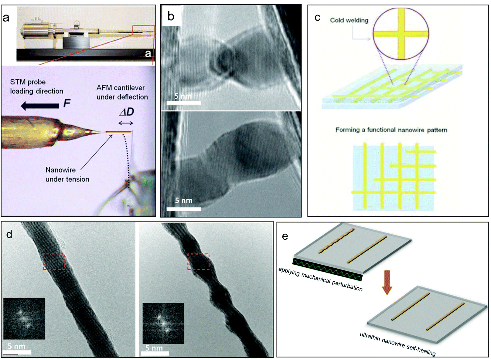 | ||
| Fig. 2 Characterization of ultrathin metallic nanowires and their device applications: (a) the in situ TEM mechanical testing of an ultrathin nanowire.22 (b) “Cold welding” of ultrathin gold nanowires2 and (c) their scalable assembly for flexible electronics. (d) “Rayleigh instability” of ultrathin gold nanowires upon moderate heating,34 and (e) mechanically assisted self-healing for nanodevice recovery.35 | ||
As the critical feature sizes of modern electronic devices continue to shrink, ultrathin metallic nanowires, in which diameters approach the sub-10 nm regime, have emerged as a new kind of 1D metallic crystals. Due to their exceedingly small sizes, the reliability of ultrathin NWs in the functional devices has become a great issue, as both theoretical predictions and experimental observations have indicated that the deformation mechanisms of ultrathin NWs can be radically different to their larger counterparts. For example, a transition from ductile to brittle fractures was observed for ultrathin gold NWs,29 which would greatly influence the reliability of devices. Apart from the deformation mechanisms, some unique behaviors are also very important for the usage of ultrathin NWs. The phenomenon called “cold welding” is found in ultrathin gold NWs with diameters ranging from 3 to 10 nm, as shown in Fig. 2(b), and this process does not need heating or high load, which gives it potential applications in the future bottom-up assembly of metallic 1D nanostructures and next-generation interconnects for extremely dense logic circuits. Moreover, the cold welding of ultrathin metallic nanowires also allows them to be used to fabricate flexible transparent films, such as gold NW networks for use in flexible electronics and biointegrated electronics, as shown in Fig. 2(c).30–33 Another interesting phenomenon is called the “Rayleigh instability,” which indicates that the morphologies of ultrathin NWs can be dramatically changed when subjected to moderate heating, as shown in Fig. 2(d), which may impede their applications as interconnects.34 However, upon random mechanical perturbation of the NWs, the phenomenon of Rayleigh instability and other damages can be healed in situ (Fig. 2(e)). Therefore, as the size of the critical components in integrated circuits approach sub-10 nm, even the inner structures and surface morphologies of ultrathin NWs are more prone to be damaged in practical services. However, with a mechanically assisted self-healing mechanism, people can directly repair defective ultrathin metallic NWs inside functional nanowire-based devices.35
Lastly, for many flexible electronics and mechatronics applications that involve cyclic loading, the repetitive straining conditions during long-term service require a comprehensive understanding of their fatigue behavior. Therefore, recently researchers have started to pay attention to the fatigue testing of NWs. For example, a novel high-cycle bending and torsion straining micromachine, based on a digital micromirror device (DMD), has been developed for the bending or torsional fatigue study of various 1D nanostructures.36 The millions of independent movable micromirrors on a single DMD chip make the platform particularly suitable for high-throughput fatigue testing.37 For low-cycle fatigue study, our patented micro-mechanical device (MMD) actuated by a quantitative nanoindenter within a high-resolution SEM could provide critical insights into the deformation and failure mechanisms of metallic nanowires under cyclic straining.11
One-dimensional covalent crystalline materials
Covalent crystals refer to a class of crystalline solids in which the atoms are bonded by covalent bonds in a continuous network extending throughout the entire material. Some of them are well-known semiconductor materials, such as pure crystals of silicon (Si), germanium (Ge), while many others are in fact seen as more attractive in recent years as “wide-bandgap semiconductors”, such as cubic boron nitride (c-BN) and silicon carbide (SiC), as well as diamond. Because of their strong and directional covalent bonding nature, they are usually very hard and brittle at the macroscopic scale, but recent studies have suggested that micro/nanosized covalent crystals can withstand extremely large deformation without mechanical inelastic relaxation or failure compared with their conventional counterparts. This is because of the nature of covalent bonding, and as fewer defects exist inside the nanoscale sample so that the inelastic deformation can be suppressed greatly under confining loading conditions. Si NW is one of the most important 1D covalent crystalline materials because of its availability and attractive physical properties, which are vital for applications in nanoelectronics and nanoelectromechanical system devices as well as for other functional applications. Recent in situ TEM tensile research has shown that VLS-growth single crystalline Si NWs with diameters of ∼100 nm exhibit >10% elastic strain at room temperature, which is getting close to the theoretical elastic limit.3Fig. 3a shows the basic configuration of the tensile testing, and the result shows that the Si NW can fully recover its original length after strain values were applied of up to 13% (Fig. 3b), showing its value for potential applications such as epidermal electronics, flexible electronics, and recent bio-nano interfaces,38–41 which involve large deformation. Another important covalent crystalline material is diamond, the hardest natural and extreme material with high carrier mobility, in where negative or positive carriers of electric current can move freely through it and which has a multitude of applications in high-frequency electronic devices and power electronics. However, the disadvantages of its poor deformability and high brittleness seriously affect its functional applications. Recently, research has shown that single crystalline diamond nanoneedles can undergo elastic bending deformation approaching the theoretical elastic strain limit of diamond (9%).4 As shown in Fig. 3(c and d), by developing a unique nanoindenter-based push-to-bend testing method, we were able to demonstrate that a diamond nanoneedle can fully recover after ultralarge bending deformation without fracture, suggesting entirely new applications for nanodiamonds.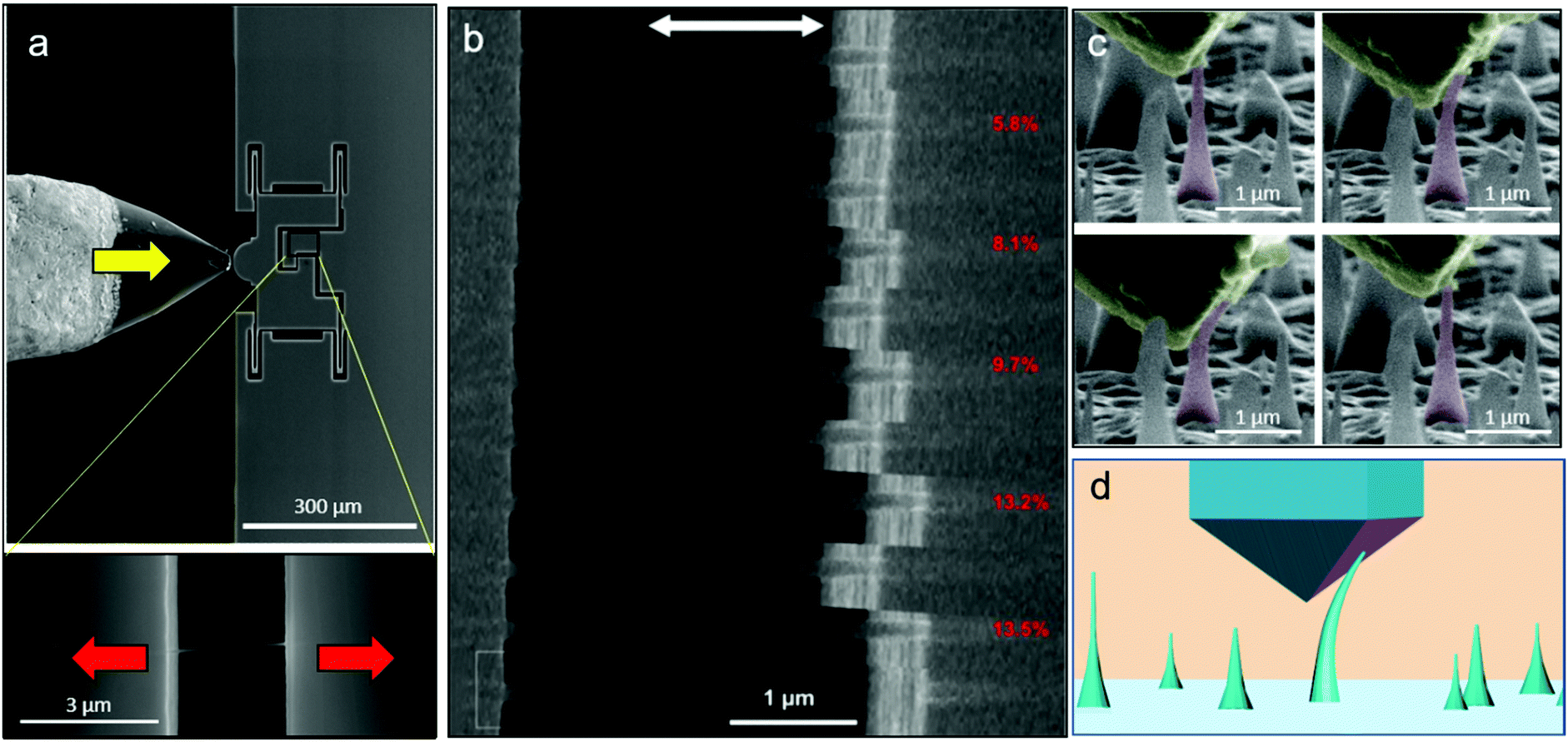 | ||
| Fig. 3 Ultralarge elasticity in nanoscale covalent crystals: (a) the in situ SEM tensile testing of a single nanowire based on a push-to-pull micromechanical device (MMD).3 (b) Loading–unloading cyclic test of a VLS-grown silicon nanowire showing near ideal elastic limit. (c) Fully recoverable bending deformation of a diamond nanoneedle by a (d) nanoindenter-induced bending test.4 | ||
Not limited to elemental covalent crystal 1D nanomaterials, compound covalent nanostructures have also been found to have a much larger deformation ability as compared with their bulk counterparts. For example, elastic strains of ∼2%42 and 4.5%43 were respectively found in SiC NWs through in situ tensile tests, which are close to the theoretical value (5%) obtained by first principle calculations.43 The elastic behavior of different types of single crystal GaAs NWs, another important third-generation semiconductor material, has been investigated by in situ TEM compression tests,44 showing fracture strains as high as 10%. Overall, it has been proved that at the nanoscale, covalent crystal nanostructures’ deformability is much better than their bulk counterparts, in particular their elasticity, due to the difficulty to enter into plastic deformation as in the cases of metallic nanowires. Combined with their unique band structures, these nanomechanical behaviors provide the foundation to experimentally achieve “strain engineering,” or ESE, which demonstrates the potential to significantly accelerate the engineering of exotic electronic properties in ordinary materials via large elastic/lattice strains: by applying just a bit of strain to a piece of covalent crystalline material, researchers can deform the orderly arrangement of atoms in its structure enough to cause dramatic changes in its properties, such as the way it conducts electricity, transmits light, or conducts heat. In fact, the potential commercial value of strain engineering has been already demonstrated by the billion-dollar strain-Si semiconductor industry, in which even 1% strain in silicon processor chips can in some cases improve the speed of the device by 50%, by allowing electrons to move through the material much faster. Some recent research studies have been done and demonstrated the potential for ESE to dramatically improve the device performance; for example, Cui et al. discovered that the carrier mobility change could result in a giant piezoresistance effect in p-type Si nanowires during stretching.38 Another example is that a recent calculation suggested that the bandgap structure of germanium (Ge) could be fundamentally changed by a large tensile strain, changing from an indirect bandgap to a direct bandgap.45
Thus, understanding the nanomechanical properties of 1D covalent crystalline solids is not only important for the reliability and properties of different kinds of micro/nanomechanical devices and MEMS, but also brings about new possibilities and solutions for creating materials tuned precisely for electronic, optoelectronic, and photonic devices that could find uses for communications, information processing, and energy applications based on ESE. These studies also provide theoretical and experimental support, so that novel functional properties based on exotic properties through extremely strained covalent crystalline materials for highly tunable electronic and optoelectronic devices can be developed in the near future. 1D covalent crystals, such as diamond and SiC, could even make a difference in the emerging “quantum computing” field, because of the diamond nitrogen-vacancy center and silicon-vacancy related defects in hexagonal polytypes as leading qubit candidates.46,47
Similarly, ionic crystals, due to their bonding nature, share a lot of similar mechanical properties, such as high brittleness, but are less strong. Some studies have already been done on ionic nanomaterials, for example, tension and buckling tests have been done to investigate the elastic and failure properties of ZnO NWs,48 while the Young's modulus and the bending strength of CuO and ZnO NWs were measured with an in situ SEM technique.49
Two-dimensional crystalline materials
Since the discovery of graphene, a single layer of carbon atoms arranged in a hexagonal lattice,50 more and more other 2D layered materials have been discovered and fabricated in the past decades,51 including black phosphorous or phosphorene, hexagonal boron-nitride (h-BN), transition metal-dichalcogenides (TMDs), metal oxides, graphitic carbon nitride (g-C3N4), and MXenes.52 2D metal nanomaterials have also received extensive research interest because of their anisotropic structure, and promising applications in catalysis, bioimaging, sensing, and solar cells.53 MXene is a new member in the class of 2D materials, and are promising candidates in the fields of sensors, catalysts, and batteries due to their metallically conductive and hydrophilia natures.54 Because of the unusual and excellent physical, chemical properties of 2D materials, such as high electron mobility, high strength, high transmittance, and high thermal conductivity,55,56 they can be the ideal candidates for the fabrication of next-generation thinner and faster electronic and optoelectronic components, such as transistors, transparent touch screens, light panels, and solar cells.57,58 Either being structural components or functional devices, mechanical loading and deformations, like bending, distortion, vibration, and thermal expansion, are often involved in their real device applications during service. Therefore, it is crucial to obtain a clear understanding of the mechanical properties and deformation behavior of 2D crystalline materials for the reliability of different functional applications. However, the current understanding of their mechanical property and physic-chemical performance under loading is limited since experimental studies on 2D materials still face challenges, i.e., material preparation and transfer, need for suitable clamping device, in situ characterization, etc., and this is also the reason for the fact that there are some computational research studies published but few experiments.Despite the experimental mechanical study of 2D materials remaining extremely challenging, exciting progress has been made in the past decades. Different methods to explore the mechanical properties of these materials have been developed, such as atomic force microscopy (AFM)-based nanoindentation tests, pressurized blister tests or bulge tests, and micromechanical testing device-based tests. Lee et al. were the first to report research into the measurement of the elastic properties of an intrinsic fracture strength of free-standing monolayer graphene with the AFM nanoindentation technique, as shown in Fig. 4a.59 According to their report, the Young's modulus and intrinsic strength of the graphene were 1 TPa and 130 GPa, respectively. With the same method, the elastic stiffness, intrinsic strength, and mechanical behavior of polycrystalline graphene films grown by chemical vapor deposition (CVD) were studied.60 The same experiments by AFM nanoindentation were also conducted to explore the mechanical properties and strain engineering of other 2D materials, such as MoS261 and h-BN,62 and the results showed the local max strain of both could be very high (0.25 for MoS2 and 0.22 for h-BN). Despite the success of the AFM-based nanoindentation test, pressurized blister tests or bulge tests were also developed for testing such ultrathin film layers. The interlayer shear stress of bilayer graphene was first measured based on pressurized microscale bubble loading devices, as shown in Fig. 4b.63 The biaxial straining of a suspended monolayer MoS2 was conducted by Lloyd et al.64 Some indirect methods have also been developed to test the tensile property of 2D crystalline materials, such as by depositing them on the surface of flexible PDMS thin film (Fig. 4c) and then testing them by conducting conventional tensile tests. Recently, Zhang et al. used a microfabricated micromechanical device (MMD), as shown in Fig. 4d, to measure the fracture toughness of CVD-synthesized graphene with a pre-crack65 in a general agreement with Griffith theory.66 A brittle fracture was observed after applying a load with a pre-crack introduced by FIB, and the fracture morphology was shown. By using a similar micromechanical device, the tensile fracture behaviors of multi-layer graphene and MoS2 membranes were also studied by Li et al., with Fig. 4e and f showing the morphologies of the samples upon fracture.67
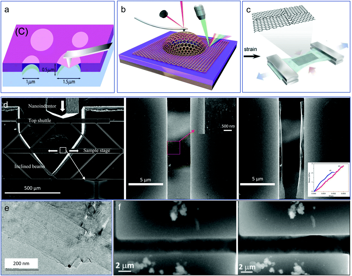 | ||
| Fig. 4 Nanomechanics of 2D materials: (a) measuring the intrinsic mechanical properties of suspended graphene by AFM indentation.59 (b) Measuring the interlayer shear stress of bilayer graphene based on pressurized microscale bubble loading.63 (c) Tensile testing of graphene films on PDMS substrate; (d) MMD-based fracture testing of graphene with pre-crack.65 (e) Our in situ TEM fracture testing of multilayer graphene films, and (f) tensile testing of a free-standing MoS2 nanosheet.67 | ||
Similar to covalent crystals, the elastic straining of 2D crystals can also be a practical and facile strategy for adjusting the bandgap and for engineering the electronic properties. Thus the so-called strain engineering or ESE of 2D materials has attracted more and more research efforts in recent years.68,69 For example, by a performing first-principle density functional theory (DFT) calculations in zigzag BN nanoribbons upon elastic strain, their bandgap could be significantly tuned, resulting from a reduced orbital hybridization;70 Andres et al. recently controlled the band structure of MoS2 through local-strain engineering for tailoring the optoelectronic properties of MoS2;69 Levy et al. explored the strain-induced pseudo-magnetic field in strained graphene nanobubbles.68 However, this emerging field needs to be further explored with joint efforts from mechanical engineers, materials scientists, and physicists. A recent example is how twisted bilayer graphene demonstrated a tunable bandgap structure71 and superconductivity,71 suggesting that there is still big room to explore unprecedent functional applications based on the nanomechanical manipulation of existing 2D materials.
Conclusions
Low-dimensional crystalline nanomaterials, including 1D metallic nanomaterials, covalent nanocrystals, and 2D materials, are promising functional materials and consequently have attracted the attention of numerous researchers, and their studies are raising new possibilities for the development of low-dimensional materials-based functional devices, including flexible electronics/energy devices nanoelectronics, optoelectronics, and nanoelectromechanical system (NEMS) devices. Despite this, even though this paper could only review some of the recent experimental research studies concerning a few representative low-dimensional crystalline nanomaterials, we found that they can have a huge impact in associated functional applications, which will provide critical insights for the future development of robust nanodevices and industrial applications. In addition, this Focus article demonstrates the new opportunities brought about by “strain engineering” (or ESE) and its related novel functional applications. The ESE of low-dimensional crystalline materials is very difficult to be realized experimentally since it requires ultrastrength materials to sustain very large elastic strain and the precise manipulation and mechanical straining of low-dimensional materials. Recently, given the advances in synthesis and the explosive proliferation of nanomaterials with “ultra-strength” together with the rapid development of experimental nanomechanical techniques reported here, ESE has now become an experimental reality, which will open up new potential functional applications of low-dimensional crystalline materials, such as energy conversion, photocatalysis, and optical interconnects, based on the fact that strain engineering allows properties such as bandgap structure and spectral absorption to be changed on the fly. Scientifically, the in situ nanomechanical experiment results will greatly complement the theoretical and modeling efforts in solid mechanics at the small scale, and together they should provide unprecedented detail and quantitative insights into how nanomaterials respond to applied loads with desired functional properties and thus allow us to theoretically and experimentally identify “strain-tuned” nanomaterials with exotic, highly tunable, functional properties toward electronic, optoelectronic, and spintronic device applications. Thus, the future research into low-dimensional crystalline materials should be closely related to ESE (even the catalytic performances of metallic nanocrystals can be tuned by elastic strain72) and the use of new technologies, such as artificial intelligence and machine learning, to guide strain engineering, whereby a material's properties and performance could be designed and engineered.73 Overall, the nanomechanics of low-dimensional crystalline materials remains fascinating and of great importance for their reliable, robust, and high performance functional applications, and can provide unpreceded opportunities in the future development of nanotechnology.Conflicts of interest
The authors declare that they have no competing interests.Acknowledgements
The authors acknowledge the financial supports from Hong Kong Research Grant Council (RGC) under the GRFs CityU 11216515 and CityU 11207416, as well as the City University of Hong Kong under SRGs 7004857 and 7005070 and National Natural Science Foundation of China (51805420).Notes and references
- C. M. Lieber, MRS Bull., 2003, 28, 486–491 CrossRef CAS.
- Y. Lu, J. Y. Huang, C. Wang, S. Sun and J. Lou, Nat. Nanotechnol., 2010, 5, 218 CrossRef CAS PubMed.
- H. Zhang, J. Tersoff, S. Xu, H. Chen, Q. Zhang, K. Zhang, Y. Yang, C.-S. Lee, K.-N. Tu and J. Li, Sci. Adv., 2016, 2, e1501382 CrossRef PubMed.
- A. Banerjee, D. Bernoulli, H. Zhang, M.-F. Yuen, J. Liu, J. Dong, F. Ding, J. Lu, M. Dao and W. Zhang, Science, 2018, 360, 300–302 CrossRef CAS PubMed.
- X. Li, H. Gao, C. J. Murphy and K. Caswell, Nano Lett., 2003, 3, 1495–1498 CrossRef CAS.
- P. Li, Q. Liao, S. Yang, X. Bai, Y. Huang, X. Yan, Z. Zhang, S. Liu, P. Lin and Z. Kang, Nano Lett., 2014, 14, 480–485 CrossRef CAS PubMed.
- J.-H. Seo, Y. Yoo, N.-Y. Park, S.-W. Yoon, H. Lee, S. Han, S.-W. Lee, T.-Y. Seong, S.-C. Lee and K.-B. Lee, Nano Lett., 2011, 11, 3499–3502 CrossRef CAS PubMed.
- J. Song, X. Wang, E. Riedo and Z. L. Wang, Nano Lett., 2005, 5, 1954–1958 CrossRef CAS PubMed.
- B. Wang, H. Zhang, J. Lou and Y. Lu, Mater. Res. Lett., 2017, 6, 13–21 Search PubMed.
- C. Jiang, H. Lu, K. Cao, W. Wan, Y. Shen and Y. Lu, Scanning, 2017, 2017, 6215691 Search PubMed.
- H. Zhang, C. Jiang and Y. Lu, Exp. Mech., 2017, 57, 495–500 CrossRef CAS.
- T. A. Schaedler, A. J. Jacobsen, A. Torrents, A. E. Sorensen, J. Lian, J. R. Greer, L. Valdevit and W. B. Carter, Science, 2011, 334, 962–965 Search PubMed.
- L. Gao, J. Song, Z. Jiao, W. Liao, J. Luan, J. U. Surjadi, J. Li, H. Zhang, D. Sun and C. T. Liu, Adv. Eng. Mater., 2018, 20, 1700625 Search PubMed.
- M. D. Uchic, D. M. Dimiduk, J. N. Florando and W. D. Nix, Science, 2004, 305, 986–989 CrossRef CAS PubMed.
- J. Y. Kim, D. Jang and J. R. Greer, Acta Mater., 2010, 58, 2355–2363 Search PubMed.
- T. Zhu, J. Li, A. Samanta, A. Leach and K. Gall, Phys. Rev. Lett., 2008, 100, 025502 CrossRef PubMed.
- J. R. Greer, W. C. Oliver and W. D. Nix, Acta Mater., 2005, 53, 1821–1830 CrossRef CAS.
- C. R. Weinberger and W. Cai, Proc. Natl. Acad. Sci. U. S. A., 2008, 105, 14304–14307 Search PubMed.
- Z. Shan, R. K. Mishra, S. S. Asif, O. L. Warren and A. M. Minor, Nat. Mater., 2008, 7, 115 CrossRef CAS PubMed.
- H. Cho, K. Hemker, K. Lian, J. Goettert and G. Dirras, Sens. Actuators, A, 2003, 103, 59–63 Search PubMed.
- Z. Yong, Q. Qin, X. Feng, F. Fan, D. Yong, T. Zhang, B. J. Wiley and L. W. Zhong, Phys. Rev. B: Condens. Matter Mater. Phys., 2012, 85, 045443 CrossRef.
- Y. Lu, J. Song, J. Y. Huang and J. Lou, Nano Res., 2011, 4, 1261–1267 CrossRef CAS.
- Y. Yue, P. Liu, Z. Zhang, X. Han and E. Ma, Nano Lett., 2011, 11, 3151–3155 Search PubMed.
- Q. Wang, J. Wang, J. Li, Z. Zhang and S. X. Mao, Sci. Adv., 2018, 4, eaas8850 CrossRef PubMed.
- L. Hu, H. S. Kim, J.-Y. Lee, P. Peumans and Y. Cui, ACS Nano, 2010, 4, 2955–2963 CrossRef CAS PubMed.
- C.-J. Lee, K. H. Park, C. J. Han, M. S. Oh, B. You, Y.-S. Kim and J.-W. Kim, Sci. Rep., 2017, 7, 7959 CrossRef PubMed.
- S. Han, S. Hong, J. Ham, J. Yeo, J. Lee, B. Kang, P. Lee, J. Kwon, S. S. Lee and M. Y. Yang, Adv. Mater., 2014, 26, 5808–5814 CrossRef CAS PubMed.
- S. Hao, L. Cui, D. Jiang, X. Han, Y. Ren, J. Jiang, Y. Liu, Z. Liu, S. Mao and Y. Wang, Science, 2013, 339, 1191–1194 CrossRef CAS PubMed.
- K. Cao, Y. Han, H. Zhang, L. Gao, H. Yang, J. Chen, Y. Li and Y. Lu, Nanotechnology, 2018, 29, 295703 Search PubMed.
- H. Wu, D. Kong, Z. Ruan, P.-C. Hsu, S. Wang, Z. Yu, T. J. Carney, L. Hu, S. Fan and Y. Cui, Nat. Nanotechnol., 2013, 8, 421 CrossRef CAS PubMed.
- C. F. Guo, Y. Lan, T. Sun and Z. Ren, Nano Energy, 2014, 8, 110–117 CrossRef CAS.
- A. Miyamoto, S. Lee, N. F. Cooray, S. Lee, M. Mori, N. Matsuhisa, H. Jin, L. Yoda, T. Yokota and A. Itoh, Nat. Nanotechnol., 2017, 12, 907 Search PubMed.
- S. Lee, D. Sasaki, D. Kim, M. Mori, T. Yokota, H. Lee, S. Park, K. Fukuda, M. Sekino and K. Matsuura, Nat. Nanotechnol., 2019, 14, 156 CrossRef CAS PubMed.
- S. Xu, P. Li and Y. Lu, Nano Res., 2018, 11, 625–632 CrossRef CAS.
- B. Wang, Y. Han, S. Xu, L. Qiu, F. Ding, J. Lou and Y. Lu, Small, 2018, 14, 1704085 CrossRef PubMed.
- C. Jiang, D. Hu and Y. Lu, Micromachines, 2016, 7, 49 CrossRef PubMed.
- C. Jiang, H. Zhang, J. Song and Y. Lu, Extreme Mech. Lett., 2018, 18, 79–85 CrossRef.
- T. Bozhi, L. Jia, D. Tal, J. Lihua, J. H. Tsui, Q. Quan, S. Zhigang, L. Robert, D. S. Kohane and C. M. Lieber, Nat. Mater., 2012, 11, 986–994 CrossRef PubMed.
- R. He and P. Yang, Nat. Nanotechnol., 2006, 1, 42 CrossRef CAS PubMed.
- D.-H. Kim, N. Lu, R. Ma, Y.-S. Kim, R.-H. Kim, S. Wang, J. Wu, S. M. Won, H. Tao and A. Islam, Science, 2011, 333, 838–843 CrossRef CAS PubMed.
- Y. Qin, X. Wang and Z. L. Wang, Nature, 2008, 451, 809 CrossRef CAS PubMed.
- Y. Zhang, X. Han, K. Zheng, Z. Zhang, X. Zhang, J. Fu, Y. Ji, Y. Hao, X. Guo and Z. L. Wang, Adv. Funct. Mater., 2007, 17, 3435–3440 CrossRef CAS.
- W. Lambrecht, B. Segall, M. Methfessel and M. Van Schilfgaarde, Phys. Rev. B: Condens. Matter Mater. Phys., 1991, 44, 3685 CrossRef CAS.
- B. Chen, J. Wang, Q. Gao, Y. Chen, X. Liao, C. Lu, H. H. Tan, Y.-W. Mai, J. Zou and S. P. Ringer, Nano Lett., 2013, 13, 4369–4373 CrossRef CAS PubMed.
- K. Guilloy, N. Pauc, A. Gassenq, Y.-M. Niquet, J.-M. Escalante, I. Duchemin, S. Tardif, G. Osvaldo Dias, D. Rouchon and J. Widiez, ACS Photonics, 2016, 3, 1907–1911 Search PubMed.
- J. Weber, W. Koehl, J. Varley, A. Janotti, B. Buckley, C. Van de Walle and D. D. Awschalom, Proc. Natl. Acad. Sci. U. S. A., 2010, 107, 8513–8518 Search PubMed.
- V. Ivády, J. Davidsson, N. T. Son, T. Ohshima, I. A. Abrikosov and A. Gali, Phys. Rev. B, 2017, 96, 161114 Search PubMed.
- F. Xu, Q. Qin, A. Mishra, Y. Gu and Y. Zhu, Nano Res., 2010, 3, 271–280 CrossRef CAS.
- B. Polyakov, L. Dorogin, S. Vlassov, M. Antsov, P. Kulis, I. Kink and R. Lohmus, Eur. Phys. J. B, 2012, 85, 366 CrossRef.
- K. S. Novoselov, A. K. Geim, S. V. Morozov, D. Jiang, Y. Zhang, S. V. Dubonos, I. V. Grigorieva and A. A. Firsov, Science, 2004, 306, 666–669 CrossRef CAS.
- A. Gupta, T. Sakthivel and S. Seal, Prog. Mater. Sci., 2015, 73, 44–126 CrossRef CAS.
- C. Tan, X. Cao, X.-J. Wu, Q. He, J. Yang, X. Zhang, J. Chen, W. Zhao, S. Han and G.-H. Nam, Chem. Rev., 2017, 117, 6225–6331 CrossRef CAS PubMed.
- Y. Chen, Z. Fan, Z. Zhang, W. Niu, C. Li, N. Yang, B. Chen and H. Zhang, Chem. Rev., 2018, 118, 6409–6455 CrossRef CAS.
- M. Naguib, V. N. Mochalin, M. W. Barsoum and Y. Gogotsi, Adv. Mater., 2014, 26, 992–1005 CrossRef CAS PubMed.
- X. Li, W. Cai, J. An, S. Kim, J. Nah, D. Yang, R. Piner, A. Velamakanni, I. Jung and E. Tutuc, Science, 2009, 324, 1312–1314 CrossRef CAS.
- D. L. Duong, G. H. Han, S. M. Lee, F. Gunes, E. S. Kim, S. T. Kim, H. Kim, Q. H. Ta, K. P. So and S. J. Yoon, Nature, 2012, 490, 235 CrossRef CAS.
- A. K. Geim and K. S. Novoselov, Nanoscience and Technology: A Collection of Reviews from Nature Journals, World Scientific, 2010, pp. 11–19 Search PubMed.
- K. S. Novoselov, V. Fal, L. Colombo, P. Gellert, M. Schwab and K. Kim, Nature, 2012, 490, 192 CrossRef CAS PubMed.
- C. Lee, X. Wei, J. W. Kysar and J. Hone, Science, 2008, 321, 385–388 CrossRef CAS PubMed.
- G.-H. Lee, R. C. Cooper, S. J. An, S. Lee, A. Van Der Zande, N. Petrone, A. G. Hammerberg, C. Lee, B. Crawford and W. Oliver, Science, 2013, 340, 1073–1076 CrossRef CAS.
- R. C. Cooper, C. Lee, C. A. Marianetti, X. Wei, J. Hone and J. W. Kysar, Phys. Rev. B: Condens. Matter Mater. Phys., 2013, 87, 035423 CrossRef.
- L. Song, L. Ci, H. Lu, P. B. Sorokin, C. Jin, J. Ni, A. G. Kvashnin, D. G. Kvashnin, J. Lou and B. I. Yakobson, Nano Lett., 2010, 10, 3209–3215 CrossRef CAS.
- G. Wang, Z. Dai, Y. Wang, P. Tan, L. Liu, Z. Xu, Y. Wei, R. Huang and Z. Zhang, Phys. Rev. Lett., 2017, 119, 036101 CrossRef.
- D. Lloyd, X. Liu, J. W. Christopher, L. Cantley, A. Wadehra, B. L. Kim, B. B. Goldberg, A. K. Swan and J. S. Bunch, Nano Lett., 2016, 16, 5836–5841 CrossRef CAS.
- P. Zhang, L. Ma, F. Fan, Z. Zeng, C. Peng, P. E. Loya, Z. Liu, Y. Gong, J. Zhang and X. Zhang, Nat. Commun., 2014, 5, 3782 CrossRef CAS PubMed.
- S. S. Terdalkar, S. Huang, H. Yuan, J. J. Rencis, T. Zhu and S. Zhang, Chem. Phys. Lett., 2010, 494, 218–222 CrossRef CAS.
- P. Li, C. Jiang, S. Xu, Y. Zhuang, L. Gao, A. Hu, H. Wang and Y. Lu, Nanoscale, 2017, 9, 9119–9128 RSC.
- N. Levy, S. Burke, K. Meaker, M. Panlasigui, A. Zettl, F. Guinea, A. C. Neto and M. Crommie, Science, 2010, 329, 544–547 CrossRef CAS.
- A. Castellanos-Gomez, R. Roldán, E. Cappelluti, M. Buscema, F. Guinea, H. S. van der Zant and G. A. Steele, Nano Lett., 2013, 13, 5361–5366 CrossRef CAS.
- J. Qi, X. Qian, L. Qi, J. Feng, D. Shi and J. Li, Nano Lett., 2012, 12, 1224–1228 CrossRef CAS PubMed.
- Y. Cao, V. Fatemi, S. Fang, K. Watanabe, T. Taniguchi, E. Kaxiras and P. Jarillo-Herrero, Nature, 2018, 556, 43 CrossRef CAS PubMed.
- L. Wang, Z. Zeng, W. Gao, T. Maxson, D. Raciti, M. Giroux, X. Pan, C. Wang and J. Greeley, Science, 2019, 363, 870–874 CrossRef CAS PubMed.
- Z. Shi, E. Tsymbalov, M. Dao, S. Suresh, A. Shapeev and J. Li, Proc. Natl. Acad. Sci. U. S. A., 2019, 116, 4117–4122 CrossRef CAS.
Footnote |
| † These authors contributed equally to this work. |
| This journal is © The Royal Society of Chemistry 2019 |