DOI:
10.1039/C9NH00042A
(Communication)
Nanoscale Horiz., 2019,
4, 969-974
Tight-binding modeling of excitonic response in van der Waals stacked 2D semiconductors
Received
22nd January 2019
, Accepted 26th February 2019
First published on 26th February 2019
Abstract
Atomically thin transition metal dichalcogenides (TMDCs) exhibit fascinating excitonic properties which are of critical importance for potential applications in nanoscale optoelectronics. In particular, stacked TMDC layers without lattice mismatch allow modulation of their band structures and optoelectronic properties through manipulation of the constituent materials along the stacking direction. Current understanding of TMDC layer-by-layer structures is mainly based on optical measurements and DFT calculations. In this work, we use a phenomenological tight-binding model, combined with DFT calculations, to understand the measured layer-dependent excitonic response of WS2. This explicit and effective model can quantitatively predict the layer-dependent excitonic states and can also be used to study interlayer excitons (direct and indirect exciton states) in TMDC multilayer structures. In addition, we find that the temperature dependence of the A exciton emission energy of monolayer WS2 can be well described with the Varshni formula, and that the emission intensity variation with temperature is associated with thermal redistribution of exciton population and increased non-radiative damping due to the enhanced electron–phonon interaction at elevated temperatures.
Conceptual insights
The GW approximation and Bethe–Salpeter equation (BSE) methods are regarded as standard means to numerically predict excitonic effects in van der Waals (vdW) stacked two-dimensional (2D) transition metal dichalcogenides (TMDCs), and their results are highly consistent with optical measurements. Despite the success of GW and BSE, an intuitive model is needed to capture the essential physics of the exciton–photon interaction in these stacked vdW structures under various conditions. A common model used to study the layer-dependent shift of excitonic energy is the quantum-well model with fractional-dimensional space. Although this model can fit the excitonic layer-dependence well with some tuning parameters, it barely reflects the nature of TMDC vdW bonds. Here, we use a phenomenological tight-binding model, combined with DFT calculations, to understand the measured layer-dependent excitonic response of WS2. This simple yet effective model can quantitatively predict layer-dependent excitonic properties and be used to study interlayer excitons in TMDC heterostructures. In addition, we find that the temperature dependence of the A exciton emission energy of monolayer WS2 can be well described with the Varshni formula, and the temperature-induced emission intensity variation is associated with thermal redistribution of the exciton population and increased non-radiative damping due to the enhanced electron–phonon interaction at elevated temperatures.
|
Introduction
Transition metal dichalcogenides (TMDCs), with the generalized formula MX2 where M = Mo, W, or Pt, and X = S, Se, or Te, have attracted a great deal of fundamental research and interest for technological applications. Two-dimensional (2D) MX2 is formed as a sandwich structure with chalcogen atoms in two hexagonal planes separated by a plane of metal atoms. In particular, monolayer MX2 materials exhibit direct band gaps in the visible and near-infrared region, making them ideal candidates as complementary metal oxide semiconductors. Due to the atomic thickness of 2D TMDCs, the dielectric screening effect is significantly suppressed, and is more than one order of magnitude weaker than that of bulk GaAs, leading to a dominant excitonic response at room temperature. The strong electron–hole interactions in these materials have triggered numerous studies in the context of many-body physics.1–4 In addition to the influence on electronic states of many-electron systems, their optical properties have also attracted great attention. For instance, the breaking of inversion symmetry in odd-layer TMDCs enables control of the valley polarization with circularly polarized light5–10 and strong excitonic second-harmonic generation.11–16 It has been clearly shown that the stacking of 2D materials with van der Waals (vdW) bonds has a prominent effect on excitonic emission. A vdW heterostructure, which is deterministically formed by stacking different types of 2D materials together, can also exhibit new properties, such as long-lived interlayer excitons,17,18 tunneling transistors, and light-emitting tunneling diodes, which are all absent in their constituent layers. Recently, layer-dependent ferromagnetism in a vdW CrI3 2D material (ferromagnetism in the monolayer, anti-ferromagnetism in the bilayer, and then back to ferromagnetism in the trilayer), which is not affected by the substrate coupled with it, has been predicted19 and observed.20,21 Nowadays, numerical studies of exciton states with GW and Bethe–Salpeter equation (BSE) methods are regarded as a standard way to describe semiconductor excitonic effects, and their results are highly consistent with optical measurements of various 2D materials.22,23 Despite the success of the GW and BSE methods in calculating exciton states in 2D materials, an intuitive model, which can capture the essential physics of 2D layer-by-layer structures, is needed to understand the physical mechanisms of light–exciton interactions in these structures under different conditions.
In this work, we characterize the number of layers in WS2 through examining their breathing modes in the low wavevector region, which indicates the vdW nature between WS2 layers.24 We then examine the layer-number-dependent A and B excitons with differential reflection spectroscopy. The extracted layer-dependent exciton resonance energies can be well described with an intuitive tight-binding model, which demonstrates a more general interpretation of the layer-dependent optical properties of WS2 than the quantum well model with fractional-dimensional space. Finally, we observe an obvious temperature-dependent polaron effect on the photoluminescence emission energy and intensity of monolayer WS2, consistent with the Varshni formula and the physical scenario of the thermal redistribution of the exciton population, which reveals the similarity between the excitonic states in WS2 and the electronic levels of traditional semiconductors.
Experimental
Synthesis
Monolayer and few-layer WS2 triangular flakes were synthesized on 0.35 mm thick sapphire (Al2O3) substrates by chemical vapor deposition (CVD) reaction of WO3 and sulfur. A sapphire wafer was first diced into 1 × 1 cm2 pieces, washed in an ultrasonic bath with acetone and isopropanol, and then blow dried with UHP nitrogen gas. Subsequently, WO3 thin films were transferred into a quartz tube reactor for sulfurization for 60 min at 30 Pa and ∼900 °C. A mixed Ar and H2 flow (8![[thin space (1/6-em)]](https://www.rsc.org/images/entities/char_2009.gif) :1 in volume flow rate) was used to convey the WO3−x vapor species to the downstream substrates, and S vapor was generated from S powders placed upstream from a lower temperature region (∼100 °C) which was controlled independently.
:1 in volume flow rate) was used to convey the WO3−x vapor species to the downstream substrates, and S vapor was generated from S powders placed upstream from a lower temperature region (∼100 °C) which was controlled independently.
Characterization
Raman spectra were recorded under excitation at 488 and 633 nm to determine the thicknesses of the WS2 flakes. Photoluminescence spectra from excitation at 488 and 532 nm as well as differential reflectance spectra were measured to study the thickness-dependent excitonic energies. The 532 and 633 nm lasers were installed in a confocal optical microscope system (NT-MDT NTEGRA Spectra Solar), and the laser beams were focused on the sample surface by a 100× objective (N/A = 0.90). Optical spectra from excitation at 488 nm were obtained on a micro-Raman spectrometer (HORIBA HR800), and the laser beam was illuminated onto the sample through a 100× objective (N/A = 0.80). Differential reflectance is defined as δR = RW/RS − 1, where RW and RS are the reflected light intensities from the sapphire substrate with and without the WS2 flakes, respectively.25,26 In the differential reflectance measurements, broadband white light from a tungsten quartz halogen source was focused on the sample by a 100× objective (N/A = 0.80); reflected signals were collected with the same objective and delivered to a CCD camera (Pixis 400) equipped with a spectrometer (Princeton Instrument, SP-2300) for spectral analysis. In the Raman measurements, the on-focus beam radius was about 1 μm which is smaller than the typical size of each layer region (larger than 2 μm in general). In the reflectance measurement, we used a weakly focused white light with a typical beam spot size of more than 100 μm to illuminate the flakes, and the reflectance from each layer region was measured by putting a pin hole in the image plane to restrict the region for signal collection. The corresponding measurement region was also about 1 μm.
Computational methods
Density functional theory (DFT) calculations based on the conventional Kohn–Sham Hamiltonian were performed using the Perdew–Burke–Ernzerhof (PBE) local density approximation (LDA).
Results and discussion
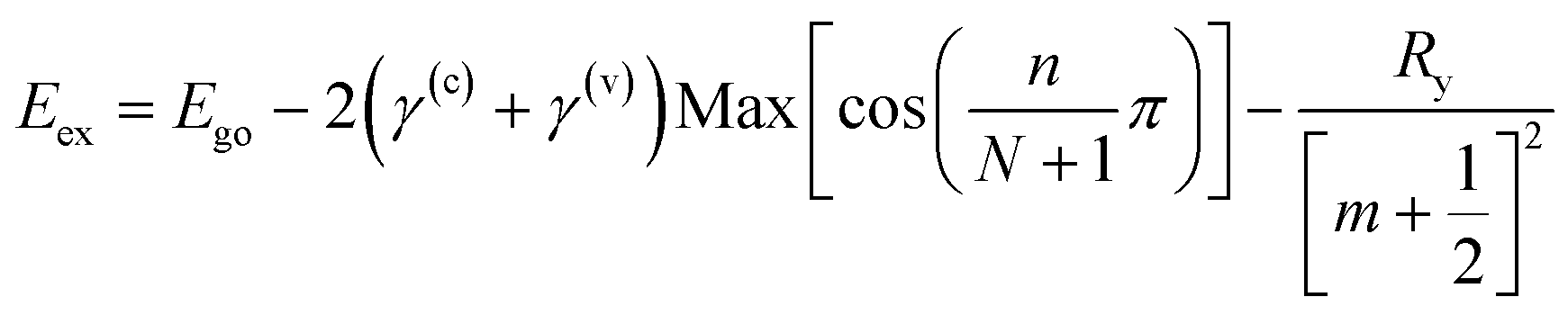
Fig. 1(a) shows the optical photograph of a CVD-grown WS2 island on a sapphire substrate, which exhibits monolayer, bilayer, multilayer, and bulk grains. The specific thicknesses (i.e., layer numbers) of this flake are determined with confocal Raman measurements. Fig. 1(b) shows the corresponding Raman mapping of the A1g peak intensity at 633 nm excitation, which demonstrates significant variation in Raman intensity over different grains. Low-frequency Raman spectra for points 1, 2, 3, 4, 5 and 6 as denoted in Fig. 1(a) are presented in Fig. 1(c). One traditional means of confirming the layer numbers of WS2 is the use of the high-frequency Raman modes, E12g and A1g, excited at a 488 nm wavelength. Differing from the high-frequency Raman modes, low-frequency Raman spectra disclose more remarkable layer dependence, as presented in Fig. 1(c). The Raman peaks at ∼32 cm−1 and ∼18 cm−1 observed for the bilayer grain undergo red shift as the layer number increases, and they appear at ∼12 cm−1 and ∼7 cm−1 for the 5-layer flake. In accordance with the previously observed softening trend of Raman modes in MoS2 and MoSe2 with increasing layer number,24,27,28 we tentatively assign these two Raman peaks to the B1 and B2 layer breathing modes,24 which are closely related to the number of layers of WS2.
 |
| | Fig. 1 (a) Bright-field optical image and (b) corresponding A1g Raman intensity mapping of a WS2 island flake; (c) low-frequency Raman spectra of the WS2 island measured from points 1, 2, 3, 4, 5 and 6 as denoted in (a) under 488 nm excitation, which correspond to the 1L, 2L, 3L, 4L, 5L, 6L and the bulk WS2 regions. | |
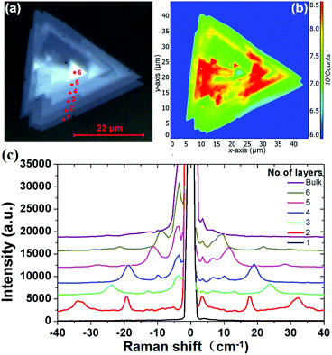
Fig. 2(a) shows the differential reflectance spectra of a WS2 flake with different layer numbers. Two absorption peaks from the monolayer region can be observed at ∼1.98 and ∼2.36 eV, which correspond to the A and B excitonic energies, respectively. They arise from the direct gap transitions at the K (K′) points of the first Brillouin zone.29 As the layer number increases, both A and B excitons gradually shift to lower energies. For the bulk WS2 region, the A and B excitonic peaks shift to ∼1.86 and ∼2.23 eV, respectively.
 |
| | Fig. 2 (a) Differential reflectance spectra of a WS2 island flake with different layer numbers; (b) measured peak positions of A and B 1s state excitons with fitting curves from eqn (3). The symbols are experimental data, and the dotted lines are the fitting results using eqn (4); (c) photoluminescence spectra of the same flake under 488 nm excitation; (d) and (e) are atomic structures of WS2 for the DFT calculations; (f) calculated layer-number-dependent energy band structures, where the vertical axis is the energy in eV. | |
Fig. 2(b) summarizes the peak positions of A and B excitons. It seems that the energy difference between the A and B peaks remains approximately 400 meV for all layers, in accordance with the spin–orbit splitting energy in the valence band of WS2.30
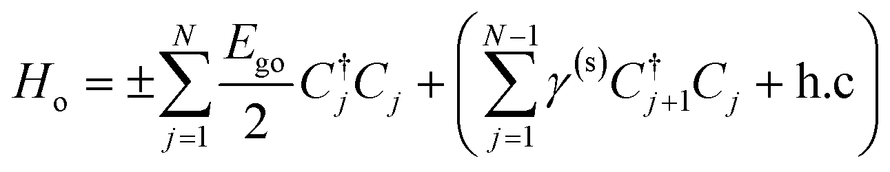
A common model used to study the layer-dependent shifts of excitonic energies in 2D TMDCs is the quantum well model with fractional-dimensional space.31 Although this model can fit the layer-number-dependent excitonic resonance energies well with some tuning parameters, it cannot reflect the nature of the vdW interlayers in which the potential energy is inhomogeneous across the structure. By making good use of the weak vdW bonds between layers, we can use single-layer valence and conduction bands to span the basis of the Hamiltonian of a vdW interlayer structure. The tight-binding model is applicable to vdW interlayers with finite extension of the wave function between interlayer atoms. This model has been widely used to calculate the band structure of graphene vdW interlayers.31–33 Under these conditions, similar to the case of the conduction band of black phosphor vdW interlayers,36 here we employ a phenomenological tight-binding model used for open-ended linear chain systems to model the TMDC vdW interlayer structures:
| | 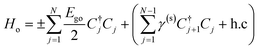 | (1) |
where
Ego is the bandgap of the single-layer WS
2, and
γ(s) is the interlayer hopping constant. As a result, the corresponding optical band gap (
Eg) can be determined using the open-ended tight-binding model:
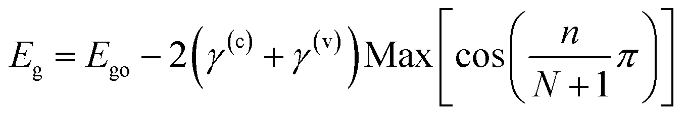
| |  | (2) |
The allowed values of n are 1, 2, 3, …, N. We further extend this model to study the excitonic effects in TMDCs. In the framework of this model, the N-layer WS2 is equivalent to a finite 1D lattice of N identical atoms with only nearest-neighbour coupling. The Hamiltonian of an exciton envelope function, φ(r), formed in a vdW interlayer structure is given by:
| |  | (3) |
where 1/
μ = 1/
mh + 1/
mv (
mh and
mv are the effective masses of the hole and electron at the valence and conduction bands, respectively), (
Eex −
Eg) =
E is the negative of the exciton binding energy and
is for a 2D system. Therefore, the corresponding transition energy of the exciton at the
K or
K′ valley (neglecting interlayer electron–hole interactions and layer-number-dependent dielectric screening effects) can be expressed as:
| |  | (4) |
where
γ(c) +
γ(v) = 0.842 eV (determined by fitting the experimental results as shown in
Fig. 2(b)), and the integers
m,
n and
N are the exciton quantum number, the interlayer state index and the number of layers, respectively, and
Ry is the Rydberg constant for the WS
2 exciton. The layer-number-dependent characteristics in
eqn (4) are valid for
n ≥ 2 and the change in optical bandgap from
n = 1 to 2 involves a direct to indirect bandgap transition (this issue will be discussed in a later section).
One can see from eqn (4) that the larger the layer number is, the lower the energy of the excitonic transition becomes, which is in agreement with the experimental results summarized in Fig. 2(b). Due to the localization of the exciton wavefunction, the ground state of the WS2 excitons (such as A and B excitons) can be approximated as the 1s state of a 2D exciton.22 However, an additional modification is needed to study the layer-dependent dielectric function for m > 1.22,23 Besides the reflectance spectra, the photoluminescence spectra shown in Fig. 3(b) (for points 1, 2, 3, 4, 5 and 6 as denoted in Fig. 1(a)) also exhibit significant layer-number dependence. Fig. 3(a) presents the corresponding emission intensity mapping of the WS2 island flake at 532 nm excitation. One can see that the PL signal intensity for n > 1 is much lower than that for n = 1 and the bulk WS2 region shows nearly no signal, which is due to the indirect bandgap nature. When an electron is excited to a higher-energy state under light illumination, it will relax to the minimum energy state via multi-phonon emission. For an indirect bandgap transition, electron–phonon interaction is required for conservation of crystal momentum. For radiative recombination to occur in an indirect band gap material, this process must also involve the absorption or emission of a phonon with a momentum equal to the crystal momentum between the electron and the hole, which is less likely to occur. This explains why PL in indirect band gap materials is much lower than in the direct band-gap transition ones. As the WS2 flake thins to a few layers, the emission intensity from direct interband transitions dramatically increases and reaches the maximum at the monolayer limit. The emission peak also shifts from ∼633 nm for the 5L WS2 to ∼620 nm for the monolayer, indicating the respective direct bandgap and indirect bandgap natures of monolayer and multilayer WS2.26,36–39 In theory, our DFT results show that the bandgap transitions from direct to indirect when the layer number changes from monolayer to multilayer, which is different from in 2D black phosphorene.32 Therefore, the decrease in both exciton energy and optical absorption per layer from mono- to bilayer is caused by the transition from an direct to indirect bandgap26,34 rather than by fractional dimensions or a drastic change in dielectric constant in multilayer samples.35 The validity of the tight-binding model can be checked with ab initio GW-BSE calculations, which explicitly include screening from the substrate and between the layers as well as self-energy and electron–hole interaction effects.36 The extraordinary layer-dependent electronic structure of WS2 vdW structures is caused by the spreading of electron wavefunction between WS2 layers. Fig. 4(a) presents the photoluminescence spectra of monolayer WS2 measured at different temperatures under 488 nm excitation. In order to clearly observe the shift of emission peaks, the spectra are vertically shifted from each other. Fig. 4(b) shows the temperature-dependent emission peak energies extracted from Fig. 4(a), and demonstrates a continuous redshift of emission energy with increasing temperature. Here the temperature-induced emission energy shift can be fitted with the Varshni formula:
| | | E(T) = Ego − αT2/(T + β) − Ry/(m + 1/2)2 | (5) |
where
Ego is the bandgap at 0 K and
α and
β are phenomenological fitting parameters.
40 By using
eqn (5) to fit the emission peak positions in
Fig. 4(b) and setting
m = 0 for the A exciton emission, we obtain
Ego −
Ry/(0 + 1/2)
2 = 2.08 eV,
α = 4.8 × 10
−4 eV K
−1 and
β = 190 K. These parameters are comparable to those reported for excitonic emissions at low temperatures.
41 Also, one can see from
Fig. 4(b) that the A exciton emission intensity reaches the maximum as the temperature increases to 353.15 K, and then gradually decreases with further increases in temperature. The initial intensity rise may originate from the redistribution of exciton population from the underlying dark exciton states to the bright A exciton states.
1,42 Once the dark exciton redistribution is saturated at fairly high temperatures, the A exciton emission may begin to suffer from larger non-radiative damping at elevated temperatures, leading to the sharp decrease in the emission intensity. In fact, both the lowering of emission intensity and broadening of emission line width with increasing temperature are expected to be accompanied by a common effect known as line broadening, which is due to the enhanced electron–phonon interaction at high temperatures. Nevertheless, the good agreement of the Varshni formula and the measured WS
2 excitonic emission energies illustrates the close connection between the excitonic response in WS
2 and the band edge tendency in traditional semiconductors. This result may originate from the shifting of the band edge of WS
2 to maintain a constant binding energy as shown in
eqn (4).
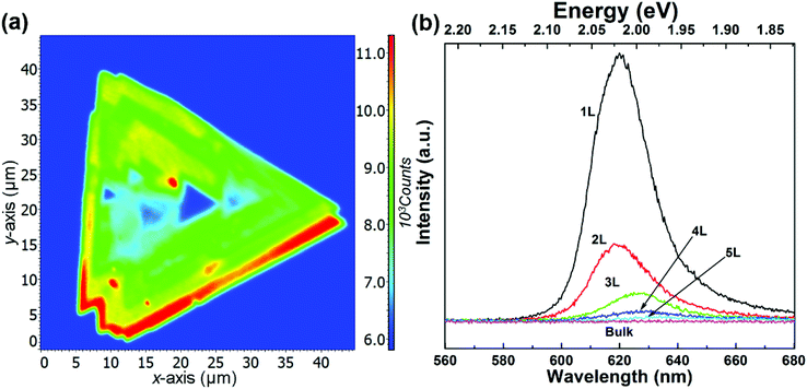 |
| | Fig. 3 (a) Fluorescence intensity map and (b) fluorescence spectra of WS2 films under 532 nm excitation. | |
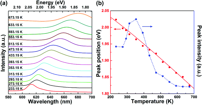 |
| | Fig. 4 (a) Temperature-dependent photoluminescence of monolayer WS2. The spectra are vertically offset from each other for clarity. (b) Emission peak position and intensity extracted from the photoluminescence spectra in (a). The solid line is the fit using the Varshni formula. | |
Conclusions
We have examined the layer-dependent excitonic response of monolayer and vdW multilayer WS2 through combining Raman, reflectance and photoluminescence imaging and spectroscopic measurements. We have observed a clear Raman breathing mode in the low-frequency Raman spectra of multilayer WS2, whose Raman shift allows rapid and unambiguous identification of the number of WS2 layers. We have used a tight-binding model, combined with DFT calculations, to semi-analytically understand the layer-dependent excitonic states in multilayer WS2. This simple yet effective model can quantitatively predict the layer-dependent excitonic response of WS2. We believe that an extension of this model could also be used to study interlayer excitons in general TMDC multilayer structures as well as other 2D semiconductors within the same theoretical framework. Finally, we found that the temperature-dependent emission energies of monolayer WS2 could be well described with the Varshni formula, indicating that the temperature-induced redshift in emission energy comes from the shifting of the band edge in order to maintain a constant binding energy.
Conflicts of interest
There are no conflicts to declare.
Acknowledgements
Cho Tung Yip and Huarui Sun were supported by grants from Shenzhen Municipal Science and Technology projects (grant no. JCYJ201605313001154 and no. JCYJ20160531192714636). Tsz Wing Lo and Dangyuan Lei acknowledge the Hong Kong Research Grants Council (GRF grant no. 15303718).
References
- X. X. Zhang, Y. M. You, S. Y. F. Zhao and T. F. Heinz, Phys. Rev. Lett., 2015, 115(25), 257403 CrossRef PubMed.
- Z. Ye, T. Cao, K. O'Brien, H. Zhu, X. Yin, Y. Wang, S. G. Louie and X. Zhang, Nature, 2014, 513(7517), 214 CrossRef CAS PubMed.
- F. Mahmood, Z. Alpichshev, Y. H. Lee, J. Kong and N. Gedik, Nano Lett., 2018, 18(1), 223 CrossRef CAS PubMed.
- A. Kogar, M. S. Rak and S. Vig,
et al.
, Science, 2017, 358(6368), 1315 CrossRef PubMed.
- X. Di, Y. Wang and N. Qian, Phys. Rev. Lett., 2007, 99(23), 236809 CrossRef PubMed.
- Y. Wang, X. Di and N. Qian, Phys. Rev. B: Condens. Matter Mater. Phys., 2008, 77(23), 235406 CrossRef.
- X. Di, G. B. Liu and W. X. Feng,
et al.
, Phys. Rev. Lett., 2012, 108(19), 196802 CrossRef PubMed.
- K. F. Mak, K. L. He and J. Shan,
et al.
, Nat. Nanotechnol., 2012, 7(8), 494 CrossRef CAS PubMed.
- T. Cao, G. Wang and W. P. Han,
et al.
, Nat. Commun., 2012, 3, 887 CrossRef PubMed.
- H. L. Zeng, J. F. Dai and Y. Wang,
et al.
, Nat. Nanotechnol., 2012, 7(8), 490–493 CrossRef CAS PubMed.
- G. Wang, X. Marie and I. Gerber,
et al.
, Phys. Rev. Lett., 2015, 114(9), 097403 CrossRef CAS PubMed.
- J. Yang, R. J. Xu and J. J. Pei,
et al.
, Light: Sci. Appl., 2015, 4, 312 CrossRef.
- J. Xiao, Z. L. Ye and Y. Wang,
et al.
, Light: Sci. Appl., 2015, 4, e366 CrossRef CAS.
- J. H. Chen, J. Tan and G. X. Wu,
et al.
, Light: Sci. Appl., 2019, 8, 8 CrossRef PubMed.
- M. Zhao, Z. L. Ye and R. Suzuki,
et al.
, Light: Sci. Appl., 2016, 5, e16131 CrossRef CAS PubMed.
- J. Sun, Y. J. Gu and D. Y. Lei,
et al.
, ACS Photonics, 2016, 3(12), 2434–2444 CrossRef CAS.
- P. Rivera, K. L. Seyler and H. Y. Yu,
et al.
, Science, 2016, 351(6274), 688–691 CrossRef CAS PubMed.
- P. Rivera, J. R. Schaibley and A. M. Jones,
et al.
, Nat. Commun., 2015, 6, 6242 CrossRef CAS PubMed.
- W. B. Zhang, Q. Qu, P. Zhu and C. H. Lam, J. Mater. Chem. C, 2015, 3, 12457 RSC.
- B. Huang, G. Clark and E. Navarro-Moratalla,
et al.
, Nature, 2017, 546(7657), 270 CrossRef CAS PubMed.
- C. Gong, L. Li and Z. L. Li,
et al.
, Nature, 2017, 46(7657), 265 CrossRef PubMed.
- D. Y. Qiu, F. H. da Jornada and S. G. Louie, Phys. Rev. Lett., 2013, 111(21), 216805 CrossRef PubMed.
- D. Y. Qiu, F. H. da Jornada and S. G. Louie, Phys. Rev. B, 2016, 93(23), 235435 CrossRef.
- Y. Y. Zhao,
et al.
, Nano Lett., 2013, 13(3), 1007 CrossRef CAS PubMed.
- K. F. Mak,
et al.
, Phys. Rev. Lett., 2008, 101(19), 196405 CrossRef PubMed.
- K. F. Mak, C. G. Lee and J. Hone,
et al.
, Phys. Rev. Lett., 2010, 105(13), 136805 CrossRef PubMed.
- M. O'Brien, N. McEvoy and D. Hanlon,
et al.
, Sci. Rep., 2016, 6, 19476 CrossRef PubMed.
- A. A. Puretzky, L. B. Liang and X. F. Li,
et al.
, ACS Nano, 2015, 9(6), 6333 CrossRef CAS PubMed.
- D. C. Kozawa, R. Kumar and A. Carvalho,
et al.
, Nat. Commun., 2014, 5, 4543 CrossRef CAS PubMed.
- W. J. Zhao, Z. Ghorannevis and L. Q. Chu,
et al.
, ACS Nano, 2013, 7(1), 791–797 CrossRef CAS PubMed.
- Y. L. Yu, Y. F. Yu and Y. Q. Cai,
et al.
, Sci. Rep., 2015, 5, 16996 CrossRef CAS PubMed.
- J. C. Slonczewski and P. R. Weiss, Phys. Rev., 1958, 109, 272 CrossRef CAS.
- E. McCann and V. I. Fal'ko, Phys. Rev. Lett., 2006, 96(8), 086805 CrossRef PubMed.
- M. H. Liu, P. Rickhaus and P. Makk,
et al.
, Phys. Rev. Lett., 2015, 114, 036601 CrossRef PubMed.
- J. Jung and A. H. MacDonald, Phys. Rev. B: Condens. Matter Mater. Phys., 2014, 89, 035405 CrossRef.
- L. K. Li, J. Kim and C. H. Jin,
et al.
, Nat. Nanotechnol., 2017, 12(1), 21–25 CrossRef CAS PubMed.
- B. R. Zhu, X. Chen and X. D. Cui, Sci. Rep., 2015, 5, 9218 CrossRef PubMed.
- H. L. Zeng, G. B. Liu and J. F. Dai,
et al.
, Sci. Rep., 2013, 3, 1608 CrossRef PubMed.
- G. Y. Jia, Y. Liu, J. Y. Gong, D. Y. Lei, D. L. Wang and Z. X. Huang, J. Mater. Chem. C, 2016, 4, 8822–8828 RSC.
-
D. W. Snoke, Solid State Physics Essential Concepts, Pearson Addison-Wesley, 2009 Search PubMed.
- D. Stich, J. Zhou and T. Korn,
et al.
, Phys. Rev. Lett., 2007, 98(17), 176401 CrossRef.
- T. W. Lo, Q. Zhang and M. Qiu,
et al.
, ACS Photonics, 2019, 6(2), 411–421 CrossRef CAS.
Footnote |
| † Both authors contributed equally to this work. |
|
| This journal is © The Royal Society of Chemistry 2019 |
Click here to see how this site uses Cookies. View our privacy policy here. 
 bc,
Guang Yi
Jia
bc,
Guang Yi
Jia


 is for a 2D system. Therefore, the corresponding transition energy of the exciton at the K or K′ valley (neglecting interlayer electron–hole interactions and layer-number-dependent dielectric screening effects) can be expressed as: