
Dynamic radiative tailoring based on mid-refractive dielectric nanoantennas†
Jiahao
Yan
 ,
Churong
Ma
,
Yingcong
Huang
and
Guowei
Yang
*
,
Churong
Ma
,
Yingcong
Huang
and
Guowei
Yang
*
State Key Laboratory of Optoelectronic Materials and Technologies, Nanotechnology Research Center, School of Materials Science & Engineering, Sun Yat-sen University, Guangzhou 510275, Guangdong, P. R. China. E-mail: stsygw@mail.sysu.edu.cn
First published on 4th February 2019
Abstract
Nanoantennas built by dielectric high-refractive index materials have drawn more and more attention. All-dielectric nanostructures with low loss and strong magnetic resonances are being explored based on various designs and materials. Silicon nanocavities as the most typical dielectric Mie resonators show a wide range of applications in nanophotonics and metamaterials. However, how to effectively engineer the resonant modes and how to dynamically tailor the spectrum still need to be studied. Here, we proposed mid-refractive dielectric nanostripes as a new kind of Mie resonator which can realize effective coupling between electric and magnetic resonant modes. Vanadium dioxide (VO2) was chosen to build a typical mid-refractive nanoantenna, and comparable scattering intensity and stronger scattering directivity can be obtained compared with silicon nanoantennas. When changing the temperature, the Mie resonance in an individual VO2 nanostripe changes because of the transformation of both the refractive index and extinction coefficient. Additionally, the active control of the photoluminescence (PL) intensities is realized owing to the interaction between VO2 nanostripes and tungsten disulfide (WS2) flakes. These findings suggest that mid-refractive dielectric nanoantennas with active tuning features will become an important building block of active photonic devices in the future.
Conceptual insightsSilicon and other all-dielectric materials have drawn much attention, and have shown comparable or even better performances than plasmonic materials in nanophotonics. Si nanostructures which can generate strong Mie-type magnetic and electric resonant modes have played an important role in shaping radiation patterns, building metasurfaces and metalenses and nonlinear optics. Unlike silicon, some mid-refractive index materials may possess better performance in specific fields. In this work, we systematically studied the directional scattering and resonant modes in mid-refractive dielectric nanoantennas and for the first time demonstrate the active scattering modulation and PL manipulation in the visible range based on the dielectric Mie-type resonant modes in VO2 nanostripes. Unlike the switch between metallic and insulator states in infrared and terahertz regions where the imaginary part of the permittivity goes below zero, the phase change of VO2 in the visible range can be described as a transformation between two mid-refractive states: higher and lower refractive index states. These findings show a new approach to build active nanophotonic nanoantennas. |
In recent years, silicon (Si) and other all-dielectric materials have drawn increasing attention, and have shown comparable or even better performances than plasmonic materials in nanophotonics. Si nanostructures which can generate strong Mie-type magnetic and electric resonant modes have played an important role in shaping radiation patterns,1–3 building metasurfaces and metalenses4–6 and nonlinear optics.7,8 Unlike Si, a typical high-refractive dielectric material, some mid-refractive index materials may possess better performance in specific fields. For instance, boron9 and Cu2O10,11 nanospheres exhibit more excellent unidirectional scattering in the visible range. The spectrally overlapping resonant modes in mid-refractive index materials can also realize strong coupling with excitons11 and enhance the second harmonic generation over a large spectral range.12 However, how the refractive index (n) and extinction coefficient (k) influence the optical properties of Mie resonators in detail and how the evolution of near-field and far-field features occurs have not been well studied in experiments. Moreover, how to realize the active control of dielectric nanoantennas still remains to be explored.13
For a wide variety of photonic applications, it is desirable to realize active tuning or electrical tuning. Recently, there has been rapid development in the tunable graphene devices.14–16 Furthermore, active tuning of the optical properties of Mie resonators is also desirable for a wide range of applications, including building optical circuits, and signal and information processing. Ultrafast photoexcitation17 and changing the surroundings of nanostructures18 are feasible ways to modulate their optical responses. Although active tuning has been widely investigated on metamaterials or arrays, the spectral tailoring of single nanoantennas is also important for on-chip nanoscale devices, which has not drawn much attention.19–21
Phase-change materials are ideal candidates for dynamic control in nanophotonics, which have tunable optical responses naturally. Researchers have demonstrated pronounced spectral tailoring based on VO2 using heating,22 applying voltages23 and defect engineering.24 VO2 nanostructures also act as a prototype in our study on mid-refractive dielectric nanoantennas. The change in the refractive index n from 2.6 to 1.8 as well as the variation of the extinction coefficient k from 0.6 to 0.4 around λ = 800 nm provides enough range for studying the mid-refractive dielectric nanoantennas.
Here, we systematically studied the directional scattering and resonant modes in mid-refractive dielectric nanoantennas and for the first time demonstrated the active scattering modulation and PL manipulation in the visible range based on the dielectric Mie-type resonant modes in VO2 nanostripes. Mid-refractive nanoantennas with spectrally overlapping bring unprecedented scattering and PL manipulation behaviors compared with plasmonic structures or widely used high-refractive nanostructures such as Si. Usually, VO2 under higher temperature can be regarded as a “metal” phase. The semiconductor–metal transition brings significant changes in electrical conductivity and optical properties.22,23 However, the change in electrical conductivity has little influence on the optical responses. What is more, the optical properties of “metal” phase VO2 in the visible range have less metallic features where n is larger and k is smaller. Therefore, unlike the switch between metallic and insulator states in infrared and terahertz regions where the imaginary part of the permittivity goes below zero,25,26 the phase change of VO2 in the visible range brings a new definition of the transformation between two dielectric states: higher (hr) and lower refractive index (lr) states. Both forward and backward scattering spectra and near-field distributions were analyzed based on different refractive indexes. In addition, we demonstrated the active PL manipulation of few layer WS2 using the phase change feature of VO2 nanostripes, which indicates different near field distributions of different mid-refractive states. Therefore, these findings show a new approach to build active nanophotonic nanoantennas.
Results and discussion
Si nanostructures have been regarded as a promising substitution of plasmonic nanostructures for building optical nanoantennas. Strong magnetic and electric resonant modes can be generated in Si nanostructures because of high refractive index and low loss. The schematic in Fig. 1a simply concludes the far-field features of nanoantennas made from three different materials: Si, gold (Au) and VO2. Strong resonant modes in Si nanoantennas lead to strong scattering intensity in both the forward and backward directions, however, the partially overlapped magnetic and electric resonant modes also produce directional scattering based on the Kerker effect.27 When decreasing n and slightly increasing k, resonant modes become weaker and broader. At the same time, the scattering pattern shows unidirectional features where forward scattering is dominated. Here VO2 is a typical example of mid-refractive nanoantennas. Further decreasing n and increasing k makes the nanoantennas possess more metallic properties, and Au can be regarded as an extreme case. As a plasmonic material, Au nanoantennas only have plasmon resonant modes on the surface and no magnetic resonant mode, which means that no directional scattering can be observed. Although the optical properties of plasmonic and high-refractive dielectric nanoantennas have been well studied, the studies on mid-refractive nanoantennas are still lacking.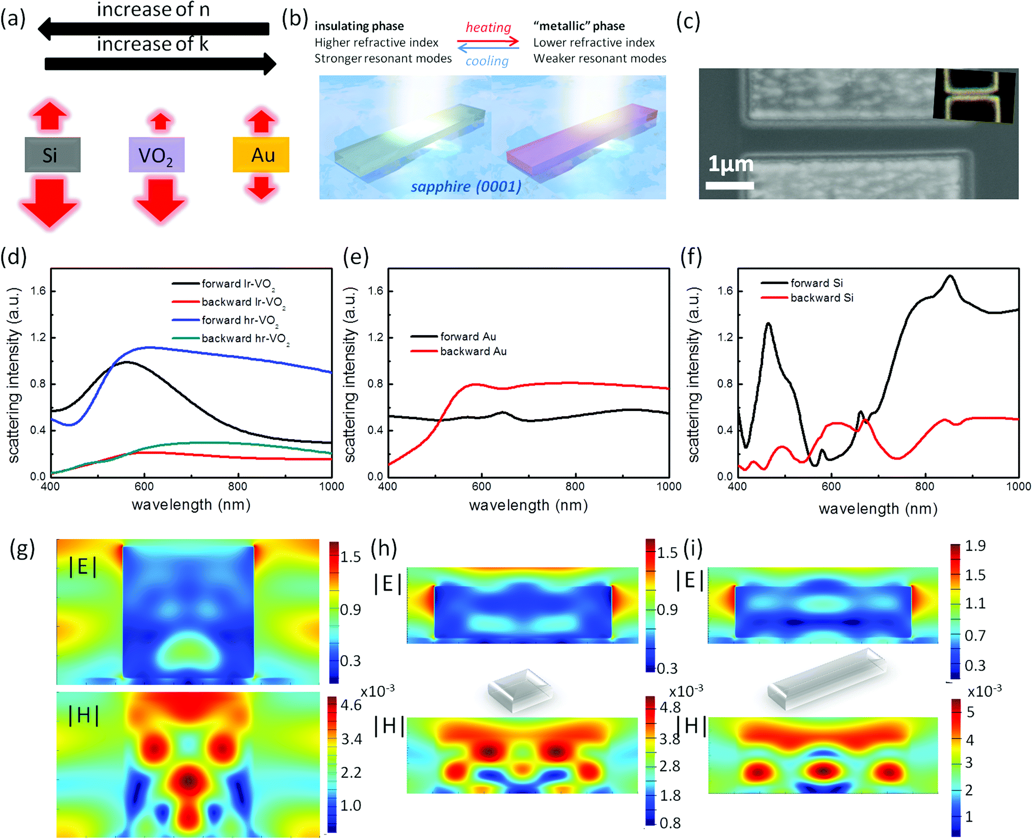 | ||
| Fig. 1 Optical properties of mid-refractive VO2 nanostripes. (a) Comparison of directional scattering among Si, VO2 and Au nanoantennas. (b) A schematic explains the differences between two states. Left is the hr-VO2 nanostripe with stronger scattering, and right is the lr-VO2 nanostripe which is lossy. (c) The SEM image of a typical VO2 nanostripe. Inset is the dark-field optical image of this nanostripe. (d) Forward and backward scattering spectra of lr-VO2 and hr-VO2 nanostripes (h = 200 nm, w = 690 nm). (e) and (f) Forward and backward scattering spectra of Au (e) and Si (f) nanostripes with the same size. (g) Electric (|E|) and magnetic field (|H|) distributions of an hr-VO2 nanostripe with the width of 445 nm and the height of 445 nm. (h) Field distributions of an hr-VO2 nanocube (width 690 nm, length 690 nm, height 200 nm). (i) Field distributions of the as-designed hr-VO2 nanostripe. | ||
VO2 as one of the phase-change materials has a metal to insulator transition (MIT) at around 68 °C. Based on the dielectric function in the visible range,26 the MIT can be treated as a transition from a higher-refractive index state to a lower-refractive index state as shown in Fig. 1b. hr-VO2 nanostructures can hold stronger resonant modes and generate stronger scattering. Using pulsed laser deposition (PLD) 28 and focused ion beam milling (FIB) techniques,29 VO2 nanostripes with different widths on Al2O3(0001) were fabricated. In Fig. 1c, the scanning electron microscope (SEM) image shows a typical VO2 nanostripe along with the optical dark-field image. Compared with Si nanostructures, VO2 nanostripes should be fabricated larger to support resonant modes because of a lower refractive index. Cross sectional SEM images in Fig. S1 (ESI†) indicate that the thickness of nanostripes is around 198 nm. The crystalline structure of the as-deposited VO2 thin films was examined by X-ray diffraction (XRD) measurements as shown in Fig. S2a (ESI†). Besides the strong diffraction peak from a substrate, two distinct peaks at 40° and 86° can be found corresponding to (020) and (040) of monoclinic VO2.28,30 The electrical properties of the fabricated VO2 film were further investigated. As a consequence, the temperature dependence of the in-plane resistance in Fig. S2b (ESI†) reveals the hysteresis loop when heating and cooling the samples. The ratio of the electrical resistance is more than 3.0 × 10².
Different scattering behaviors among Si, Au and VO2 were analyzed theoretically. In Fig. 1d–f, both forward and backward scattering spectra of nanostripes with the height of 200 nm and the width of 690 nm are presented. All curves are on the same scale to compare their intensities. For the VO2 nanostripe, scattering mainly distributes forward especially for hr-VO2. While for the Au nanostripe, little difference can be seen between forward and backward scattering after excluding substrate effects. Obvious directional scattering can also be observed in the Si nanostripe. Although the scattering intensity is stronger than both Au and VO2 nanostripes, the scattering directivity strongly depends on wavelengths because of stronger but fast-changing Mie resonant modes. For typical Si nanospheres, the interaction between electric and magnetic modes brings directional scattering where forward scattering is dominant at some wavelengths and backward scattering is dominant at other wavelengths.1,2 Meanwhile, for Si nanostripes, the existence of the Al2O3 substrate and the larger width makes the forward scattering become dominant, which generally shows unidirectional scattering behavior (see Fig. S3, ESI†). Therefore, mid-refractive nanoantennas show advantages on realizing broadband unidirectional scattering. Calculated field distributions can help one choose suitable structures for building mid-refractive nanoantennas. The field profiles of the other type of nanostripe (height 445 nm, width 445 nm) and a nanocube (height 200 nm, width 690 nm, length 690 nm) along with the as-designed nanostripe are shown in Fig. 1g–i. Based on the cross sectional field distributions, we found that the as-designed VO2 nanostripe has the highest electric and magnetic field distributions because the geometric dimensioning is beneficial for effective interaction among the multipole modes.
To understand the spectral tailoring based on mid-refractive nanoantennas and the spectral change from hr-VO2 to lr-VO2, refractive index dependent backward and forward scattering should be simulated or measured. From the simulation in Fig. 2a and b, we can see how scattering spectra and resonant modes change with different n. Using the dielectric function of hr-VO2 as a standard, a series of forward and backward scattering spectra are presented based on varied n with the step length of 0.3. In forward scattering spectra, obvious red shift can be seen with the increase of n and vice versa. The red-shift arises from red-shifted and broadened magnetic and electric modes. The shift of magnetic and electric modes can be seen more obviously in backward scattering. In addition, the backward scattering intensity increases when increasing n, which weakens the unidirectional scattering. The comparison between hr-VO2 and lr-VO2 in Fig. 1d reflects the decline process, while the comparison between hr-VO2 and Si nanostripes in Fig. 1d and e reflects the growth process. However, a magnetic and electric resonant mode can be hardly separated in VO2 nanostripes because of an irregular shape. Fortunately, one can use Mie theory to calculate the magnetic and electric dipole modes of VO2 nanospheres and expand it into the case of stripes. The calculated scattering spectra of VO2 nanospheres contributed by magnetic and electric dipole modes are presented in Fig. S4 (ESI†). Both electric and magnetic dipole modes are broad, which is similar to the case of stripes. Similarly, the red-shift of both the electric and magnetic modes is observed when changing lr-VO2 to hr-VO2, which is consistent with the analysis of nanostripes. How k influences the forward and backward scattering is also investigated as shown in Fig. 2c and d. Although hr-VO2 has low-loss features, the spectral tailoring on reducing k is still significant especially on forward scattering. Besides the enhancement of scattering intensity, multipole resonant peaks also become detached and distinct. However, increasing k has much less influence on both forward and backward scattering spectra. This phenomenon also indicates that k has little influence on the spectral tailoring based on the transition from hr-VO2 to lr-VO2.
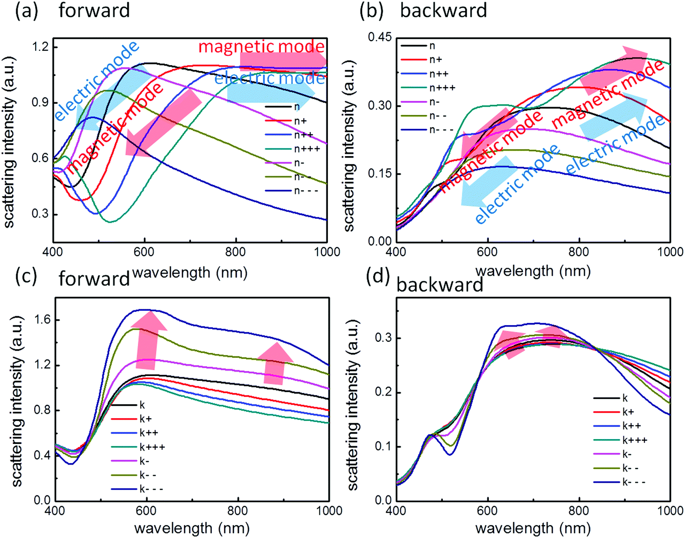 | ||
| Fig. 2 Analysis on refractive index dependent scattering spectra. (a) and (b) Forward (a) and backward (b) scattering spectra changing with the refractive index (n). Forward (c) and backward (d) scattering spectra changing with the extinction coefficient (k). | ||
To analyse the optical responses under two states experimentally, we chose two temperatures, 25 °C and 90 °C, to get steady hr-VO2 and lr-VO2 states. Fig. 3a shows the SEM images of VO2 nanostripes with different widths. The widths are 836 nm, 756 nm, 707 nm, 690 nm, 480 nm and 415 nm respectively. To increase the scattering signal contributed from Mie-type resonances, linear polarized incidence was used. An electric field with the polarization direction perpendicular to the nanostripes would experience nanoscale confinement, which is beneficial for generating Mie-type multipole resonant modes. Fig. 3b shows the experimental scattering spectra of two states. Pronounced blue-shift and lineshape change can be observed when decreasing the width of the nanostripes, because reducing the sizes brings the weakening of resonant modes. Considering that mid-refractive nanostructures hold an intrinsic broader mode, the blue-shift effect in the spectra is weaker than that of silicon nanostructures.2,9 Differences between the scattering spectra at 25 °C and 90 °C can be seen clearly especially above λ = 600 nm. Compared with the scattering spectra of hr-VO2, scattering spectra of lr-VO2 are blue-shifted and narrower. This variation trend agrees with the above analysis on different refractive indexes well. As for scattering intensities, significant contrast (close to double) can be obtained around 750 nm. This tuning effect was verified in simulation using the finite-different time-domain (FDTD) method. Dielectric functions of VO2 under two states were obtained from literature reports25,26 and fitted in software (see Fig. S5, ESI†). Simulated spectra are pretty similar to the measured spectra. Peak locations in simulation are slightly blue-shifted because the optical parameters used in simulation cannot reflect the real situation precisely. Why the measured scattering intensities around 450 nm are much higher than the simulated results is owing to the sensitivity of the detection system in the short wavelength region and the data processing. Scattering spectra of lr- and hr-VO2 nanostripes under unpolarized incidence were also measured as shown in Fig. S6 (ESI†). As we expected, the modulation depth is lower than that under linear polarized incidence.
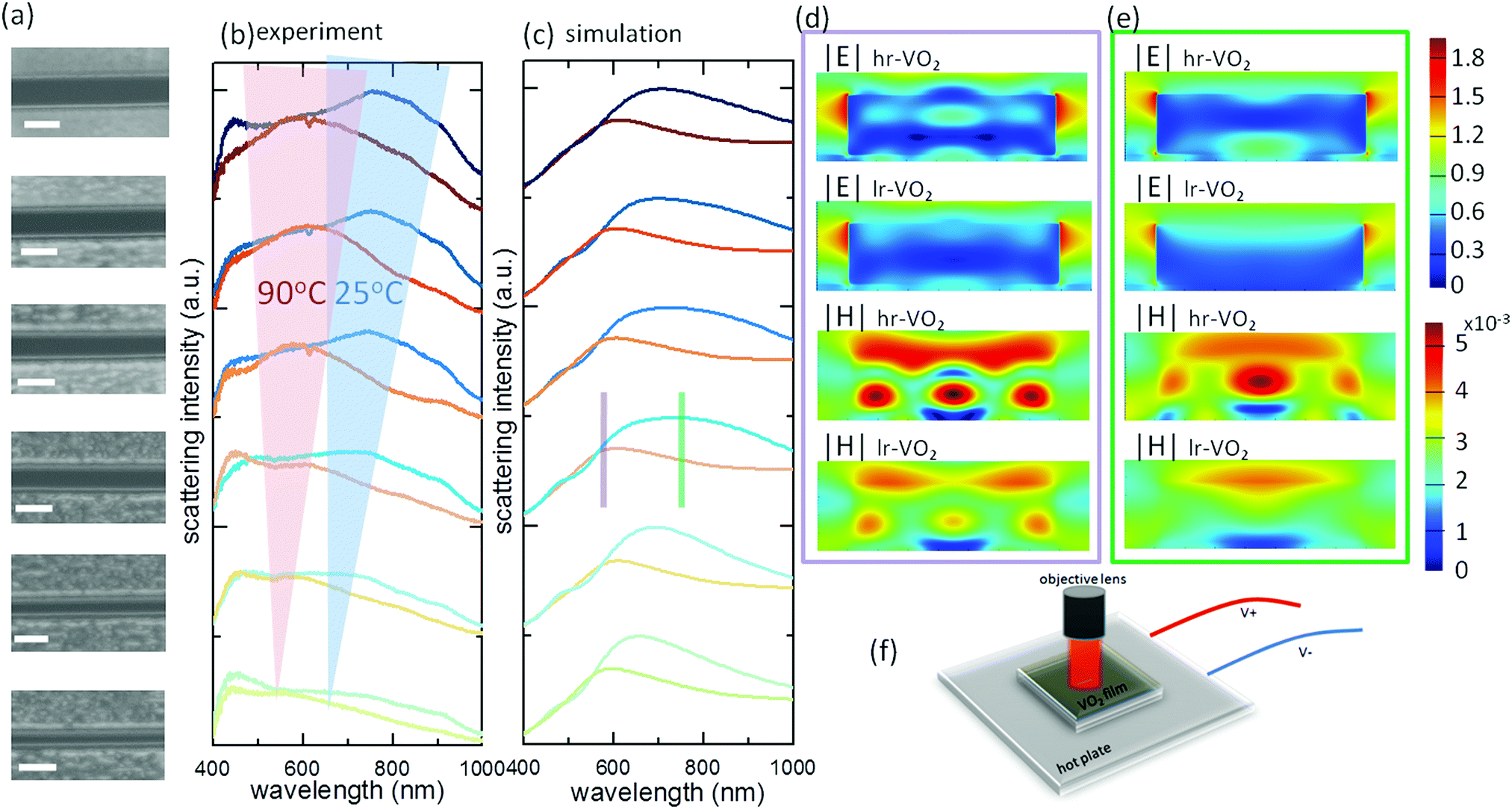 | ||
| Fig. 3 Dynamic spectral tailoring of VO2 nanostripes with different sizes. (a) High magnification SEM images of different VO2 nanostripes. The scale bars are 1 μm. (b) From top to bottom, measured scattering spectra of nanostripes when reducing widths. Cool colors represent the spectra collected at 25 °C, and warm colors represent the spectra collected at 90 °C. (c) From top to bottom, simulated scattering spectra of nanostripes when reducing widths. (d) and (e) Electric and magnetic field distributions of two states at λ = 600 nm (c) and λ = 750 nm (d). (f) A sketch of the experimental setup. | ||
The spectral differences between hr-VO2 and lr-VO2 nanostripes can be further understood through wavelength-dependent refractive index data. Although higher refractive index is favorable for realizing higher Q values, in our case, the increase of k from 700 nm to 1000 nm for lr-VO2 suppresses the scattering intensity of lr-VO2 nanostripes above 700 nm. As a consequence, the scattering spectra of lr-VO2 are narrower and blue-shifted. Calculated near-field profiles in Fig. 3d and e can further explain the mechanism of why different optical behaviors were produced. First, we compare the electric and magnetic fields at λ = 600 nm under both states. The electric field enhancement of hr-VO2 is higher than that of lr-VO2. For magnetic field distributions, circular shape regions can be observed in the cross-section of hr-VO2 which means Mie-type magnetic multipole modes are stronger. In contrast, those resonant modes are very weak in lr-VO2. At λ = 750 nm, the difference of the refractive index of both states becomes much larger, and the extinction coefficient goes higher in lr-VO2. As a consequence, for electric field distributions (see Fig. 3e), much stronger field enhancement can be obtained inside hr-VO2 nanostripes. The magnetic field profile in hr-VO2 is also a circular shape, while no circular shape magnetic field can be found in lr-VO2. This difference indicates that multipole magnetic resonant modes are much stronger in hr-VO2 nanostripes rather than lr-VO2, and stronger resonances produce much stronger scattering intensities from hr-VO2 at λ = 750 nm as marked by the green bar in Fig. 3c. The sketch in Fig. 3f shows how to heat samples and detect the active tuning scattering.
Using VO2 nanostripes can also modulate the interaction with two-dimensional materials such as WS2. A dry transfer technique was used to put WS2 flakes onto VO2 nanostripes.31 First, flakes are transferred from tape to a PDMS soft substrate. Second, the wanted flake is aligned on top of VO2 nanostripes under the microscope. Finally, PDMS is pressed and then peeled off slowly to finish the transfer process. Fig. S7 (ESI†) shows the optical images of WS2 flakes on VO2 nanostripes. The thickness of WS2 flakes can be preliminarily determined from the reflection contrast. Detailed characterizations of the WS2 flake in Fig. S7a (ESI†) are presented in Fig. 4a and b. VO2 nanostripes covered by the WS2 flake can be seen from the SEM image based on different conductivities. From the AFM topography, we found that this WS2 flake has two layers. Although bi-layer WS2 cannot produce PL as strong as a monolayer,32 it still exhibits strong emission at λ ≈ 640 nm. Because a sapphire substrate was used in PL measurement, strong PL intensity from the substrate becomes noise around λ ≈ 700 nm.33 To reduce this noise, here, we present the PL spectra of WS2 after subtracting the PL from the pure sapphire substrate as shown in Fig. 4c. Interestingly, the PL intensity at 90 °C (lr-VO2) is much larger than that at 25 °C (hr-VO2) at λ ≈ 640 nm, which is different from the situation in scattering measurement. One can notice that the PL intensity of a 90 °C sample is much larger than that of a 25 °C sample around 800 nm. This phenomenon can be understood by the interaction between excitonic emission and optical resonant modes. For example, the resonant mode from photonic crystal can change the line shape of PL emission from WSe2.34 In our case, lr-VO2 nanostripes have a weaker resonant mode especially around 800 nm (see Fig. 3). That is why a dip is observed in the PL spectrum of the 90 °C sample. Although the PL emission from WS2 around 800 nm is very weak, the Al2O3 substrate also has fluorescence as shown in Fig. S8 (ESI†). Therefore, the contrast of PL intensity at 800 nm is arising from the mixed emission signals enhanced by different resonant modes. A thicker WS2 was also investigated as shown in Fig. S7b (ESI†). Fig. 4d and e are the corresponding SEM image and AFM topography. The line profile indicates that the WS2 flake is formed by nine layers, whose property is similar to bulk WS2. Therefore, in Fig. 4f, the PL effect is dominated by the interband transition through the indirect bandgap. The PL signals at λ ≈ 875 nm are slightly different between two states. Similarly, lr-VO2 is a better choice to enhance the PL from WS2 flakes. The PL manipulation effect is much more obvious in bi-layer WS2 than that in thicker WS2 because of more effective interaction between VO2 nanostripes and WS2 flakes.
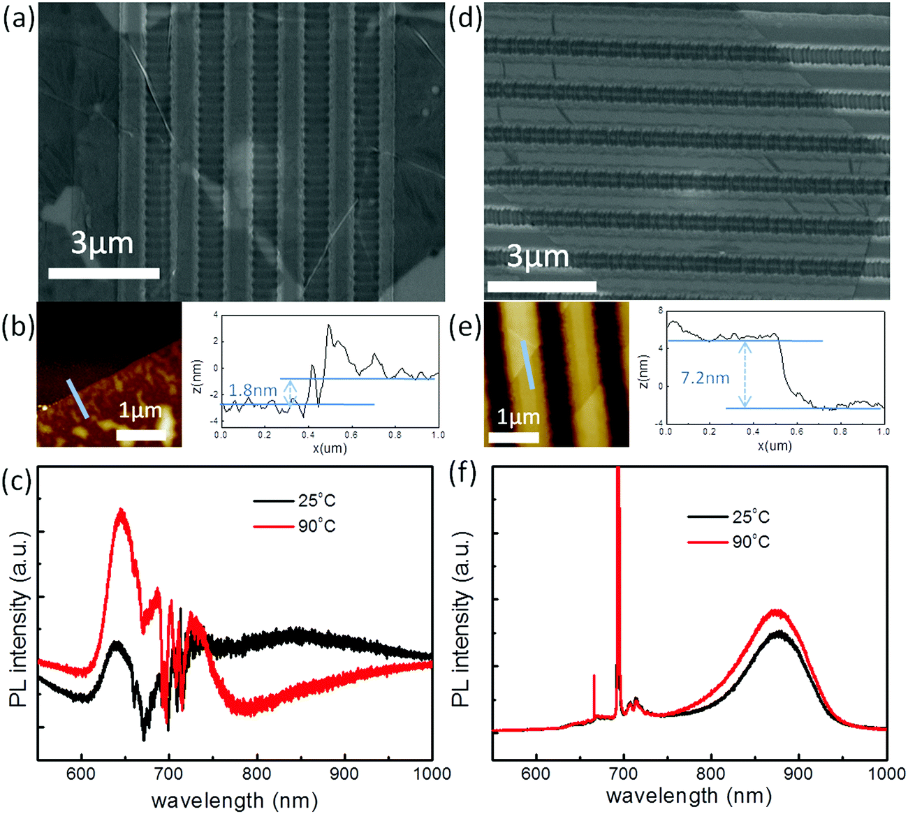 | ||
| Fig. 4 Active PL manipulation based on VO2 nanostripes. (a) and (d) SEM images of the investigated WS2 flakes. (b) and (e) AFM measurements and the corresponding height profiles along lines marked in the topographies. (c) PL intensity comparison of bi-layer WS2 on VO2 nanostripes under both states. The PL spectra have been subtracted by PL from the pure sapphire substrate. (f) PL intensity comparison of nine-layer WS2 on VO2 nanostripes under both states. | ||
Electric field distributions are plotted in Fig. 5a to illustrate why lr-VO2 brings larger PL enhancements. PL intensities are determined by the field enhancements at two wavelengths: the excitation wavelength λ ≈ 514 nm and the location of an emission peak at λ ≈ 640 nm or λ ≈ 875 nm. Since WS2 flakes are placed on top of VO2 nanostripes, the field enhancements on top of the VO2 nanostripes are what we need to analyse. At λ ≈ 514 nm, although the field profiles inside nanostripes are different because stronger Mie-type resonant modes only exist in hr-VO2 nanostripes, the field enhancements on the surface are quiet similar. However, at λ ≈ 640 nm, field distributions on the surface become different between two states. For hr-VO2 nanostripes, voids can be seen on the surface, and the distribution is fluctuant compared with that in lr-VO2 nanostripes. Similarly, at λ ≈ 875 nm, field enhancements on the top of lr-VO2 are larger than that on top of hr-VO2 nanostripes. To analyse the field enhancement on the top surface clearly, we extracted data from Fig. 5 and plotted the line-scanned field enhancements as shown in Fig. S9 (ESI†). This comparison indicates that lr-VO2 nanostripes have higher field enhancements on top-surfaces. This PL manipulation effect also verifies the field distributions of both states and helps one understand the near-field features of mid-refractive nanoantennas. The schematic in Fig. 5b summarizes the evolution of near-field distributions of nanoantennas with different n and k. Au and Si nanostripes are chosen as extreme cases, and VO2 under two states can be regarded as intermediate states partially possessing the features of both plasmonic and dielectric high-index nanoantennas. When n is large and k is small, the resonant modes are strong but concentrated inside nanostructures just like Si nanoantennas. When increasing k and decreasing n at the same time, intrinsic modes change to surface modes gradually. That is why lr-VO2 nanostripes containing more surface modes have better performance on the PL enhancement.
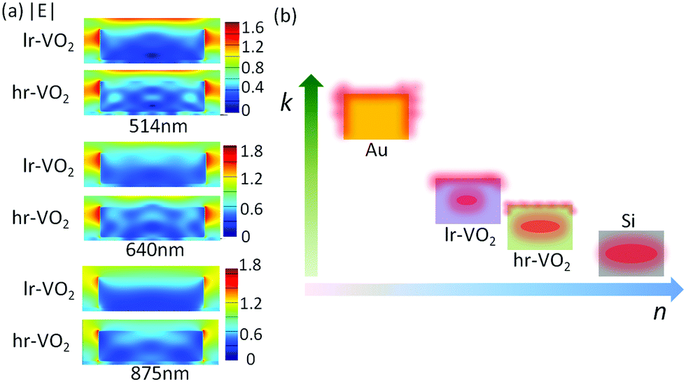 | ||
| Fig. 5 Near-field distributions of mid-refractive nanoantennas. (a) Cross sectional electric field distributions of VO2 nanostripes under two states at λ = 514 nm, λ = 640 nm and λ = 875 nm. (b) Schematic revealing the field distributions changing with refractive index n and k. Red dots indicate whether the electric field concentrates inside or on the surface for the four cases. | ||
Conclusions
In summary, we have demonstrated dynamic spectral tailoring based on mid-refractive VO2 nanoantennas. Nanoantennas based on mid-refractive materials show unique directional scattering and near-field distributions, which are different from the plasmonic and dielectric high-refractive nanostructures. The phase change of VO2 nanostripes in the visible range can be described as a switch between a higher-refractive index state and a lower-refractive index state helping us profoundly study the optical properties of mid-refractive index nanoantennas. The stronger Mie-type multipole resonant modes along with stronger scattering intensity are observed in hr-VO2 nanostripes. On the other hand, the switch between lr- and hr-VO2 can also actively manipulate the PL signals from WS2 flakes because of the dynamic control of near-field distributions. Our findings give a new insight into building nanoscale active controlled and photoelectric devices in the visible range.Methods
Device fabrication
First, the crystalline VO2 thin films were grown using a PLD method. A vanadium metal (99.99% purity) target was ablated by a KrF excimer laser pulse with a pulse rate of 4 Hz and a pulse width about 25 ns. During the deposition process, the Al2O3 (0001) substrate was kept at 550 °C in a vacuum chamber under pressure of 20 mTorr with flowing O2 (22.5 sccm) and Ar2 (15 sccm). Second, an FIB (FIB-SEM crossbeam workstation; Carl Zeiss, Auriga-4525) milling technique was used to fabricate the VO2 nanostripes. For WS2–VO2 hybrid structures, an all-dry transfer method was used to transfer WS2 flakes on the viscoelastic layer to the VO2 nanostripes under a microscope.31Scattering and PL measurements
The dark-field backward scattering spectra were obtained using a dark-field optical microscope (BX51, Olympus) integrated using a spectrograph (ISoPlane 160, Princeton Instruments) and a CCD camera (PiXis 400B-eXcelon, Princeton Instruments). During the measurements, the oblique incident white light was illuminated with a 53° incident angle on the entire nanostructures. The scattered light was collected through an objective on top (NA = 0.80) and a slit in front of the spectrograph. Heating was realized through a thin heating plate under the substrate. For PL measurements, samples were excited by a Renishaw inVia confocal Raman microscope using a 514 nm laser and a 50× objective lens (NA = 0.75) at room temperature.35,36 The signals of PL were collected using the same objective lens and then displayed using a monochromator with a grating of 1800 lines per mm.Numerical simulations
The scattering spectra and field profiles were calculated using the FDTD method (Lumerical Solution, Inc.). VO2 nanostripes were illuminated with a linear-polarized normal incident TFSF (total-field scattered-field) source (300–1100 nm). A mesh size of 3 nm for the illuminated region was utilized. The sizes of the VO2 nanostripes were set according to the experimental measurements from SEM images.Author contributions
J. H. Y., C. R. M., and Y. C. H.: experimental work. J. H. Y.: data analysis. G. W. Y.: project planning and data analysis.Conflicts of interest
There are no conflicts to declare.Acknowledgements
The National Basic Research Program of China (2014CB931700), Guangzhou city (201804020074) and State Key Laboratory of Optoelectronic Materials and Technologies supported this work.References
- J. Yan, P. Liu, Z. Lin and G. Yang, Nanoscale, 2016, 8, 5996 RSC.
- J. H. Yan, P. Liu, Z. Y. Lin, H. Wang, H. J. Chen, C. X. Wang and G. W. Yang, Nat. Commun., 2015, 6, 7042 CrossRef CAS PubMed.
- R. Camacho, M. Rahmani, S. Kruk, L. Wang, L. Xu, D. A. Smirnova, A. Solntsev, A. E. Miroshnichenko, H. H. Tan, F. Karouta, S. Naureen, K. Vora, L. Carletti, C. de Angelis, C. Jagadish, Y. S. Kivshar and D. N. Neshev, Nano Lett., 2016, 16, 7191–7197 CrossRef PubMed.
- M. Khorasaninejad, W. T. Chen, R. C. Devlin, J. Oh, A. Y. Zhu and F. Capasso, Science, 2016, 352, 1190–1194 CrossRef CAS PubMed.
- H. Liang, Q. Lin, X. Xie, Q. Sun, Y. Wang, L. Zhou, L. Liu, X. Yu, J. Zhou, T. F. Krauss and J. Li, Nano Lett., 2018, 18, 4460 CrossRef CAS PubMed.
- M. Jang, Y. Horie, A. Shibukawa, J. Brake, Y. Liu, S. M. Kamali, A. Arbabi, H. Ruan, A. Faraon and C. Yang, Nat. Photonics, 2018, 12, 84–90 CrossRef CAS PubMed.
- G. Grinblat, Y. Li, M. P. Nielsen, R. F. Oulton and S. A. Maier, Nano Lett., 2016, 16, 4635 CrossRef CAS PubMed.
- S. Liu, M. B. Sinclair, S. Saravi, G. A. Keeler, Y. Yang, J. Reno, G. M. Peake, F. Setzpfandt, I. Staude, T. Pertsch and I. Brener, Nano Lett., 2016, 16, 5426 CrossRef CAS PubMed.
- P. Liu, J. Yan, C. Ma, Z. Lin and G. Yang, ACS Appl. Mater. Interfaces, 2016, 8, 22468 CrossRef CAS PubMed.
- S. Zhang, R. Jiang, Y. M. Xie, Q. Ruan, B. Yang, J. Wang and H. Q. Lin, Adv. Mater., 2015, 27, 7432 CrossRef CAS PubMed.
- Q. Ruan, N. Li, H. Yin, X. Cui, J. Wang and H.-Q. Lin, ACS Photonics, 2018, 5, 3828 CrossRef.
- C. Ma, J. Yan, Y. Wei, P. Liu and G. Yang, J. Mater. Chem. C, 2017, 5, 4810 RSC.
- J. Yan, C. Ma, P. Liu, C. Wang and G. Yang, Nano Lett., 2017, 17, 4793 CrossRef CAS PubMed.
- X. He, P. Gao and W. Shi, Nanoscale, 2016, 8, 10388 RSC.
- X. He, F. Liu, F. Lin and W. Shi, Opt. Express, 2018, 26, 9931 CrossRef CAS PubMed.
- X. He, F. Lin, F. Liu and W. Shi, Nanotechnology, 2018, 29, 485205 CrossRef PubMed.
- S. Makarov, S. I. Kudryashov, I. Mukhin, A. Mozharov, V. Milichko, A. Krasnok and P. A. Belov, Nano Lett., 2015, 15, 6187 CrossRef CAS PubMed.
- S. Lan, S. Rodrigues, Y. Cui, L. Kang and W. Cai, Nano Lett., 2016, 16, 5074 CrossRef CAS PubMed.
- J. Kern, R. Kullock, J. Prangsma, M. Emmerling, M. Kamp and B. Hecht, Nat. Photonics, 2015, 9, 582 CrossRef CAS.
- P. Fan, Z. Yu, S. Fan and M. L. Brongersma, Nat. Mater., 2014, 13, 471 CrossRef CAS PubMed.
- F. Pyatkov, V. Futterling, S. Khasminskaya, B. S. Flavel, F. Hennrich, M. M. Kappes, R. Krupke and W. H. P. Pernice, Nat. Photonics, 2016, 10, 420 CrossRef CAS.
- Y. J. Ke, X. L. Wen, D. Y. Zhao, R. C. Che, Q. H. Xiong and Y. Long, ACS Nano, 2017, 11, 7542 CrossRef CAS PubMed.
- K. J. Miller, K. A. Hallman, R. F. Haglund Jr. and S. M. Weiss, Opt. Express, 2017, 25, 26527 CrossRef CAS PubMed.
- J. Rensberg, S. Zhang, Y. Zhou, A. S. McLeod, C. Schwarz, M. Goldflam, M. Liu, J. Kerbusch, R. Nawrodt, S. Ramanathan, D. N. Basov, F. Capasso, C. Ronning and M. A. Kats, Nano Lett., 2016, 16, 1050 CrossRef CAS PubMed.
- N. A. Butakov, I. Valmianski, T. Lewi, C. Urban, Z. Ren, A. A. Mikhailovsky, S. D. Wilson, I. K. Schuller and J. A. Schuller, ACS Photonics, 2018, 5, 371 CrossRef CAS.
- T. V. Son, K. Zongo, C. Ba, G. Beydaghyan and A. Hache, Opt. Commun., 2014, 320, 151 CrossRef CAS.
- M. Kerker, D.-S. Wang and C. L. Giles, J. Opt. Soc. Am., 1983, 73, 765 CrossRef.
- J.-H. Shin, K. Moon, E. S. Lee, I. M. Lee and K. H. Park, Nanotechnology, 2015, 26, 315203 CrossRef PubMed.
- J. Yan, C. Ma, P. Liu, C. Wang and G. Yang, Light: Sci. Appl., 2017, 6, e16197 CrossRef CAS PubMed.
- D. H. Kim and H. S. Kwok, Appl. Phys. Lett., 1994, 65, 3188 CrossRef CAS.
- A. Castellanos-Gomez, M. Buscema, R. Molenaar, V. Singh, L. Janssen, H. S. J. van der Zant and G. A. Steele, 2D Mater., 2014, 1, 011002 CrossRef.
- W. J. Zhao, Z. Ghorannevis, L. Q. Chu, M. L. Toh, C. Kloc, P. H. Tan and G. Eda, ACS Nano, 2013, 7, 791–797 CrossRef CAS PubMed.
- Y. Zhang, Y. F. Zhang, Q. Q. Ji, J. Ju, H. T. Yuan, J. P. Shi, T. Gao, D. L. Ma, M. X. Liu, Y. B. Chen, X. J. Song, H. Y. Hwang, Y. Cui and Z. F. Liu, ACS Nano, 2013, 7, 8963–8971 CrossRef CAS PubMed.
- S. Wu, S. Buckley, A. M. Jones, J. S. Ross, N. J. Ghimire, J. Yan, D. G. Mandrus., W. Yao, F. Hatami, J. Vuckovic, A. Majumdar and X. Xu, 2D Mater, 2014, 1, 011001 CrossRef.
- J. Yan, C. Ma, P. Liu and G. Yang, ACS Photonics, 2017, 4, 1092 CrossRef CAS.
- J. Yan, C. Ma, Y. Huang and G. Yang, Mater. Horiz., 2019, 6, 97 RSC.
Footnote |
| † Electronic supplementary information (ESI) available. See DOI: 10.1039/c8nh00459e |
| This journal is © The Royal Society of Chemistry 2019 |