
Additive-manufacturing of 3D glass-ceramics down to nanoscale resolution†‡
Darius
Gailevičius
 *ab,
Viktorija
Padolskytė
a,
Lina
Mikoliūnaitė
c,
Simas
Šakirzanovas
*cd,
Saulius
Juodkazis
*ef and
Mangirdas
Malinauskas
*a
*ab,
Viktorija
Padolskytė
a,
Lina
Mikoliūnaitė
c,
Simas
Šakirzanovas
*cd,
Saulius
Juodkazis
*ef and
Mangirdas
Malinauskas
*a
aLaser Research Center at Vilnius University, Sauletekio Ave. 10, Vilnius, LT-10223, Lithuania. E-mail: darius.gailevicius@ff.vu.lt; mangirdas.malinauskas@ff.vu.lt
bFemtika Ltd., Saulėtekio Ave. 15, Vilnius, LT-10224, Lithuania
cFaculty of Chemistry and Geosciences, Vilnius University, Naugarduko Str. 24, Vilnius, LT-03225, Lithuania. E-mail: simas.sakirzanovas@chf.vu.lt
dInstitute of Chemistry, Center for Physical Sciences and Technology, Sauletekio Ave. 3, Vilnius, LT-10222, Lithuania
eSwinburne University of Technology, John St., Hawthorn 3122, Vic, Australia. E-mail: sjuodkazis@swin.edu.au
fMelbourne Centre for Nanofabrication, The Victorian Node of the Australian National Fabrication Facility, 151 Wellington Rd., Clayton 3168, Vic, Australia
First published on 10th December 2018
Abstract
Fabrication of a true-3D inorganic ceramic with resolution down to the nanoscale (∼100 nm) using a sol–gel resist precursor is demonstrated. This method has an unrestricted free-form capability, control of the fill-factor, and high fabrication throughput. A systematic study of the proposed approach based on ultrafast laser 3D lithography of organic–inorganic hybrid sol–gel resin followed by a heat treatment enabled the formation of inorganic amorphous and crystalline composites guided by the composition of the initial resin. The achieved resolution of 100 nm was obtained for 3D patterns of complex free-form architectures. Fabrication throughput of 50 × 103 voxels per second is achieved; voxel – a single volume element recorded by a single pulse exposure. A post-exposure thermal treatment was used to form a ceramic phase, the composition and structure of which were dependent on the temperature and duration of the heat treatment as revealed by Raman micro-spectroscopy. The X-ray diffraction (XRD) showed a gradual emergence of the crystalline phases at higher temperatures with a signature of cristobalite SiO2, a high-temperature polymorph. Also, a tetragonal ZrO2 phase known for its high fracture strength was observed. This 3D nano-sintering technique is scalable from nanoscale to millimeter dimensions and opens a conceptually novel route for optical 3D nano-printing of various crystalline inorganic materials defined by an initial composition for diverse applications for microdevices designed to function in harsh physical and chemical environments and at high temperatures.
Conceptual insightsWe introduce a new 3D nanoscale optical printing modality for high-temperature glass-ceramic materials by combining ultrafast 3D laser nanolithography with calcination. The new pathway to inorganic 3D structures with micro- and nano-scale resolutions can be designed with a tailored final material composition. Ultrafast laser additive manufacturing allows the production of initial 3D structures with ultra-small (hundreds-of-nm) feature dimensions out of a hybrid organic–inorganic resist SZ2080. Then, post-fabrication heating (sintering) at different temperatures reaching up to 1500 °C in an air atmosphere facilitates the decomposition of the organic components resulting in the formation of a pure inorganic glass-ceramic hybrid. Calcination provides a route for the continuous size control and formation of new materials for free-form nano-/micro-objects. The application fields include tailored narrow-band IR emission sources, chemically resilient and high temperature optical elements for sensor applications in nuclear power plants, and industrial, space and defense fields where advanced nano-ceramic 3D structured materials are used. |
1 Introduction
We show that a popular hybrid organic–inorganic sol–gel resist SZ2080 can be converted into a material with entirely different properties obtained via polymer-to-ceramic transition guided by a high temperature sintering and oxidation. The silica and zirconia precursors present in the (sol–gel) resist at ∼43 wt% fraction as an inorganic component will lead to the emergence of silica and zirconia crystalline phases in the final sintered ceramic material. Importantly, a proportional downscaling of the 3D polymerized object takes place with a significant volume change of 40–50% dependent on the annealing protocol without the distortion of the size proportions of the initial 3D design. The temperature-guided resizing and the composition change can potentially be tailored to form 3D free-form patterns of complexity which is not possible using other micro-/nano-fabrication methods.In this study, we explore the possibility of applying ultrafast 3D laser nanolithography1 in conjunction with heat-treatment2 to acquire ceramic 3D structures at the micro- and nano-scale. Laser fabrication allows the production of initial 3D structures with relatively small (hundreds-of-nm) feature sizes out of hybrid organic–inorganic material SZ20803 (Fig. 1). Then, post-fabrication sintering at different temperatures up to 1500 °C in the air atmosphere facilitates the decomposition of the organic part, comprising ∼57% wt, which results in the glass-ceramic hybrid material. The resolution in the final 3D structure is superior to that of the as-fabricated structures. Both filled volume as well as complex free-form 3D objects can be resized and their structural composition changed.
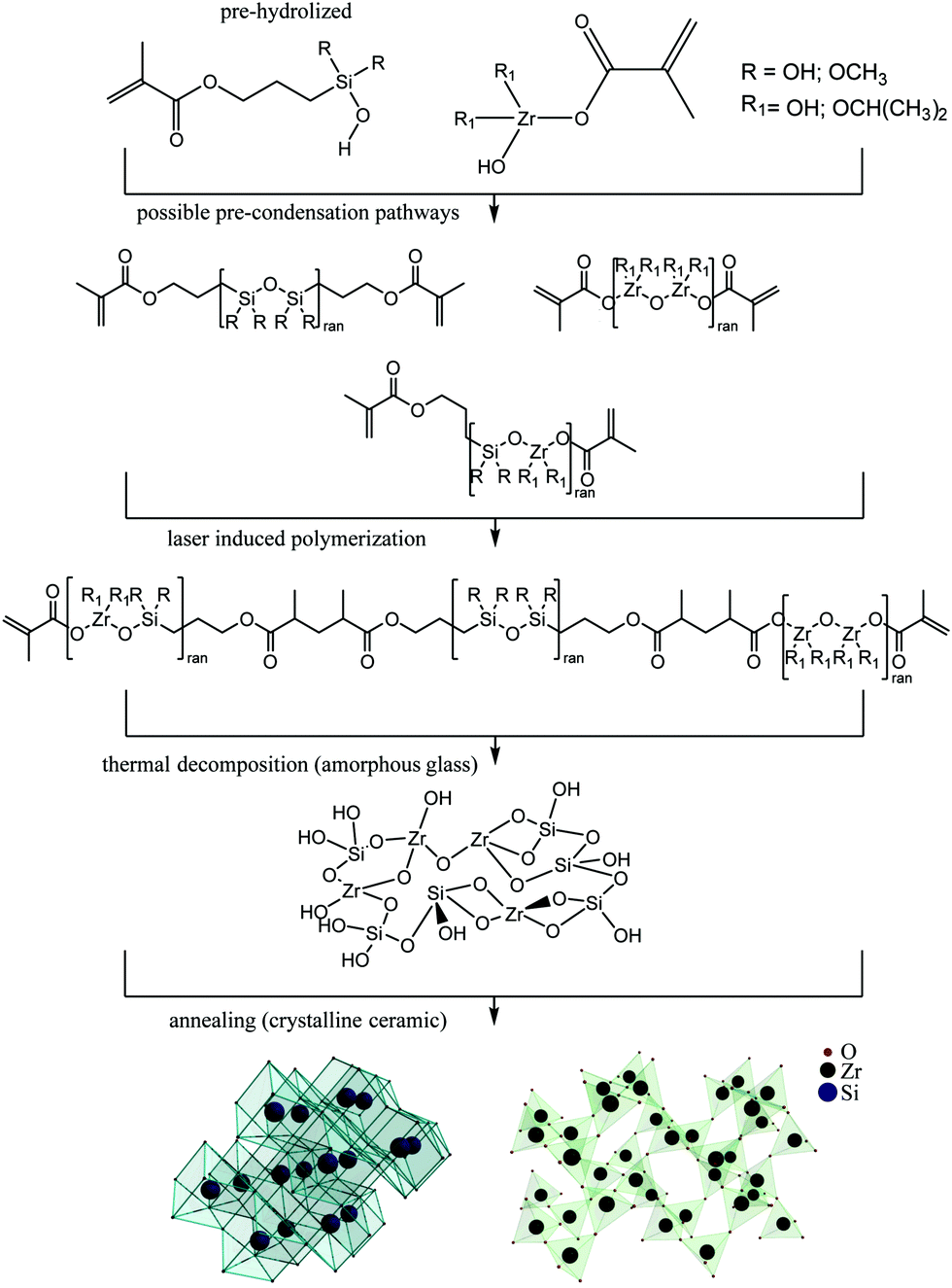 | ||
| Fig. 1 Illustration of the main steps in the synthesis of ceramics out of a hybrid SZ2080 sol–gel resist following laser induced polymerization that occurs during direct laser writing. Following the first stage of calcination, the organic part is removed from the matrix and an inorganic glass matrix is formed. As the temperature is increased further, crystallization occurs and a polycrystalline ceramic phase forms. The crystal structures of cristobalite (left) and tetragonal zirconia (t-ZrO2) (right) are shown in the bottom row. | ||
Ultrafast lasers are extending their applications towards advanced nanoscale processing of materials in additive, subtractive and combined approaches.4–7 Recently, additive manufacturing of 3D micro-/nano-structures followed by heat-treatment protocols for down-scaling their dimensions while maintaining their initial geometry was reported,8–10 yet attention was not paid to an experimentally validated explanation of the material phase conversion processes,11 and thus the potential advantages besides resizing were not investigated.12,13 Alternatively, the physical addition of metal nanoparticles resulted in roughening of the structures after turning them fully into inorganic coatings.14 This limits their applications for functional 3D nanostructures where pure inorganic materials and/or optical quality and structural uniformity of the patterns and workpieces are required.15 Lastly, up to now there has been no report on true-3D ceramic16 or glass17,18 structures with higher than tens-of-micrometers resolution despite specially designed pre-ceramic resins.19
Here, we show a straight-forward method to make 3D glass and ceramic structures with resolution down to the nanoscale with the final composition tailored by the initial materials.
2 Experimental
We used the widespread sol–gel prepolymer SZ2080 (IESL-FORTH, Greece) synthesized as described in ref. 3 for experiments of sintering/calcination. A photoinitiator was not used.2 3D laser direct written structures were fabricated from this material and heat-treatment was performed in the temperature range of 1000–1500 °C. Changes in the samples were analyzed via Raman spectroscopy and X-ray diffraction (XRD).More specifically, for our experiment, we fabricated 3D structures with different geometries. These included all-volume polymerised cubes (bulk), 3D woodpile micro lattices (periodic), free form micro-sculptures which combined bulk volumes with nanoscale features of complex geometry, and macroscopic hexagonal 3D lattices which are usually used for cell scaffolds. Laser structuring was carried out with a ∼300 fs duration, a 515 nm wavelength, and 200 kHz repetition rate pulses focused by objective lenses of different numerical apertures (NAs) from 0.8 to 1.4. Other relevant fabrication parameters were tuned to be approximately near the middle of the fabrication window,20 with one exception, where we produced a fine structure with a feature size of about ∼140 nm. This required exposure at the bottom of the fabrication window,21 which resulted in a lower cross-linking degree of the polymer matrix and increased shrinkage along with some geometrical deformation. Development of the fabricated structures was carried out in methyl-isobutyl-ketone for one hour followed by treatment in a Piranha solution to remove organic contaminants from their surface. The fragile structures were dried in a super-critical CO2 dryer to avoid mechanical changes due to capillary forces. The geometrical changes and fidelity of fabrication were tracked via optical and scanning electron microscopy (SEM).
For the (micro-)Raman spectral analysis we chose hexagonal scaffolds,22 which are easy to handle as individual workpieces, due to their millimeter scale. Micro-Raman spectra of the beams and intersections of the hexagonal scaffolds were measured at each relevant step: before and after heat treatment at different temperatures T ≤ 1500 °C. To corroborate and interpret the results we also performed an XRD analysis of the calcinated and then powdered SZ2080.
3 Results
The micro-Raman measurements are summarized in Fig. 2. As the temperature increases the spectral shape changes and evolves via qualitatively two distinct form-factors (Fig. 2). Close examination of the initial spectrum and comparison to that after annealing at T = 1000 °C reveals that they differ in molecular vibrations which can be associated with the carbon–carbon, carbon–oxygen, and carbon–hydrogen bonds. After heat-treatment these spectral lines vanish (Fig. 2b). The new spectral form coincides with that typical for silica glass; spectra of a control sample of fused silica are shown.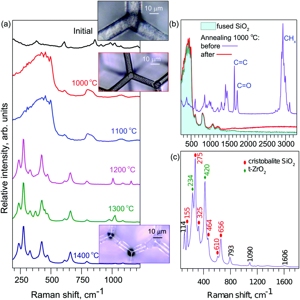 | ||
| Fig. 2 Raman spectra of laser structured SZ2080 before and after heat-treatment (for 1 h in air). The disappearance of sharp peaks represents a changed make-up of the material after heat-treatment. (a) Change in the Raman spectrum at several annealing temperatures; optical images of 3D-micro scaffolds (T = 1000, 1400 °C) from the sites where Raman spectra were measured. (b) Detailed spectrum of the initial structure and the heat treated structure at T = 1000 °C in comparison to fused silica. (c) Raman spectrum after the highest temperature T = 1400 °C annealing with peak matching to cristobalite and tetragonal zirconia (t-ZrO2). | ||
Increasing the temperature further in steps of ΔT = 100 °C results in a new qualitative change in the spectrum at T = 1200 °C. More pronounced peaks emerge with increased temperature. At the highest temperature (Fig. 2c), a few pronounced peaks become apparent. They coincide with vibrational signatures of the cristobalite23 and tetragonal zirconia24 (t-ZrO2) phases, which are formed at high temperatures.25,26
Fig. 3 shows XRD data of annealed powder samples. At the lowest treatment temperature T = 1000 °C, broad peaks indicate the formation of a glassy amorphous phase and only initial seeds of a crystalline phase. Also, the high background of the XRD signal confirms the presence of a substantial amount of amorphous material. As the temperature is increased, the peaks become exceedingly pronounced clearly showing an increasing dominance of the crystalline phase. The XRD peaks match well with reference data for cristobalite27 and tetragonal zirconia,28 proving that the annealed material is a mix of inorganic crystalline phases. From the XRD pattern, period d which corresponds to the most pronounced peaks at the diffraction angle 2θ, given by the Bragg's condition d = λ/(2![[thin space (1/6-em)]](https://www.rsc.org/images/entities/char_2009.gif) sinθ) can be estimated. The size L of the nano-crystalline phase follows from the Scherrer's equation L = Kλ/(B(2θ)cosθ); where K = 0.89 for spherical crystals and B(2θ) [rad] is the peak's angular bandwidth at the full width half maximum. The Cu Kα emission at λ = 1.5406 Å was used. The most pronounced peaks are observed after treatment at T = 1500 °C at Bragg diffraction angle 2Θ ≈ 30.14° and correspond to the crystallite size of L ≃ 117.5 nm for t-ZrO2 and similarly at the angle 2Θ ≈ 21.82° the size of the cristobalite nano-crystallites was L ≃ 30.8 nm. The size evolution of the t-ZrO2 crystallites traced by the most prominent 〈111〉 XRD peak was L ≈ 1, 14, and 118 nm as the temperature was increased to 1000, 1200, and 1500 °C, respectively.
sinθ) can be estimated. The size L of the nano-crystalline phase follows from the Scherrer's equation L = Kλ/(B(2θ)cosθ); where K = 0.89 for spherical crystals and B(2θ) [rad] is the peak's angular bandwidth at the full width half maximum. The Cu Kα emission at λ = 1.5406 Å was used. The most pronounced peaks are observed after treatment at T = 1500 °C at Bragg diffraction angle 2Θ ≈ 30.14° and correspond to the crystallite size of L ≃ 117.5 nm for t-ZrO2 and similarly at the angle 2Θ ≈ 21.82° the size of the cristobalite nano-crystallites was L ≃ 30.8 nm. The size evolution of the t-ZrO2 crystallites traced by the most prominent 〈111〉 XRD peak was L ≈ 1, 14, and 118 nm as the temperature was increased to 1000, 1200, and 1500 °C, respectively.
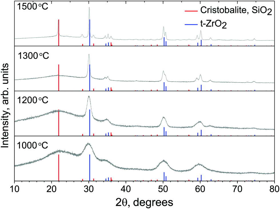 | ||
| Fig. 3 X-ray diffraction (XRD) analysis of the SZ2080 resist heat-treated at different temperatures for one hour in air at an ambient pressure. Broad peaks become more pronounced and evolve with temperature into sharp signature peaks of the two known crystalline phases of silica and zirconia. | ||
As for the geometrical stability of the structures, they retain the same proportions up to T ≤ 1200 °C, after which the structures show signs of melting and deformation. Sharp features become noticeably rounded by surface tension of the molten phase. We show that for the primary “glassy” phase, the structures retain their shape without any distortion as shown in Fig. 4. The smallest geometrical features achieved are shown in Fig. 4(d) with an average cross section of a line 85 ± 10 nm measured at the middle point between the crossing junctions. True nanoscale (sub-100 nm dimensions) resolution can be achieved by implemented processing. The effect of much higher temperatures is shown in the optical images in Fig. 2a.
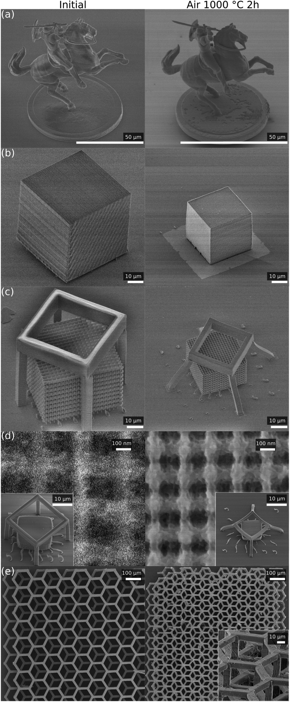 | ||
| Fig. 4 Micro-graphs of different initial and treated structures (1000 °C for 2 h). Down-sizing of solid volumetric and free-form structures with correspondingly high and low initial volume fractions of the polymer. From top to bottom: (a) a free-form sculpture of Vytis (Coat of arms of Lithuania), (b) a homogeneous cube structure, (c) large and (d) super-fine-featured photonic crystal structures with a cage, and (e) a hexagonal scaffold. | ||
4 Conclusions and outlook
It is shown that through a high-temperature calcination of 3D polymerized structures, initially made by 3D laser writing in organic–inorganic SZ2080, the polymer resist produces either a silica-based glass or a polycrystalline ceramic pure inorganic material. The glass phase dominates in the samples annealed at moderate temperatures up to ∼1200 °C. When samples are annealed above ∼1200 °C, formation of polycrystalline silica and zirconia is observed, in particular, cristobalite and t-zirconia phases.The presented modifications of silica-zirconia-rich resist SZ2080 from a glass to a polycrystalline ceramic through annealing shows a principle of thermally guided 3D material printing which can reach true nanoscale (sub-100 nm) resolution. Isotropic down-sizing of the initial 3D polymerized objects with a volume fraction of 0.5-to-1 simplifies fabrication since there is no need to alter the proportions of the initial material as it is widely used in DLW 3D nanolithography of photonic crystals, micro-optics and biomedical scaffolds in order to eliminate the effect of anisotropic shrinkage.
One can foresee a possibility to create required polymerizable mixtures which will lead to the final compounds of tailored composition, stoichiometry and size of the polycrystalline phases according to the phase diagram.29,30 Mechanical and chemical properties of the final structures and objects will acquire new features, especially resilience in harsh physical and chemical environments. Since nanoscale materials can initiate precipitation and guide the growth of nano-crystallites, the experimentation horizons are widened by the presented modality of additive manufacturing.
One can foresee an alternative controlled calcination (or pyrolysis) method for a selected and partial modification of the initially polymerised structures which undergo thermal treatment. For example, a focused electron or ion beam31 as well as focused infrared laser radiation30,32 can be used to create required seed locations where new phases with novel properties will occur after annealing. This research avenue will be explored next.
Conflicts of interest
There are no conflicts to declare.Acknowledgements
The US AMRDEC grant no. W911NF-16-2-0069 “Enhanced Absorption in Stopped-Light Photonic Nanostructures: Applications to Efficient Sensing” project is acknowledged for the financial support. SJ is grateful for the partial support via the ARC DP170100131 grant. The authors are thankful to the Dr M. Farsari group for providing the SZ2080 material and sharing information of its composition.References
- M. Malinauskas, A. Žukauskas, S. Hasegawa, Y. Hayasaki, V. Mizeikis, R. Buividas and S. Juodkazis, Light: Sci. Appl., 2016, 5, e16133 CrossRef CAS PubMed.
- L. Jonusauskas, D. Gailevicius, L. Mikoliunaite, D. Sakalauskas, S. Sakirzanovas, S. Juodkazis and M. Malinauskas, Materials, 2017, 10, 12 CrossRef PubMed.
- A. Ovsianikov, J. Viertl, B. Chichkov, M. Oubaha, B. MacCraith, I. Sakellari, A. Giakoumaki, D. Gray, M. Vamvakaki, M. Farsari and C. Fotakis, ACS Nano, 2008, 2, 2257–2262 CrossRef CAS PubMed.
- H. Wang, Y.-L. Zhang, H. Xia, Q.-D. Chen, K.-S. Lee and H.-B. Sun, Nanoscale Horiz., 2016, 1, 201–211 RSC.
- Q.-K. Li, J.-J. Cao, Y.-H. Yu, L. Wang, Y.-L. Sun, Q.-D. Chen and H.-B. Sun, Opt. Lett., 2017, 42, 543–546 CrossRef CAS PubMed.
- X.-W. Cao, Q.-D. Chen, L. Zhang, Z.-N. Tian, Q.-K. Li, L. Wang, S. Juodkazis and H.-B. Sun, Opt. Lett., 2018, 43, 831–834 CrossRef CAS PubMed.
- H. Ding, Q. Zhang, Z. Gu and M. Gu, Nanoscale Horiz., 2018, 3, 312–316 RSC.
- S. Passinger, M. Saifullah, C. Reinhardt, K. Subramanian, B. Chichkov and M. Welland, Adv. Mater., 2007, 19, 1218–1221 CrossRef CAS.
- L. Guo, H. Xia, H.-T. Fan, Y.-L. Zhang, Q.-D. Chen, T. Zhang and H.-B. Sun, Opt. Lett., 2010, 35, 1695–1697 CrossRef PubMed.
- G. Seniutinas, A. Weber, C. Padeste, I. Sakellari, M. Farsari and C. David, Microelectron. Eng., 2018, 191, 25–31 CrossRef CAS.
- J. Bauer, A. Schroer, R. Schwaiger and O. Kraft, Nat. Mater., 2016, 15, 438–443 CrossRef CAS PubMed.
- J. Li, B. Jia and M. Gu, Opt. Express, 2008, 16, 20073–20080 CrossRef CAS.
- A. Zakhurdaeva, P.-I. Dietrich, H. Hölscher, C. Koos, J. G. Korvink and S. Sharma, Micromachines, 2017, 8, 285 CrossRef PubMed.
- A. Vyatskikh, S. Delalande, A. Kudo, X. Zhang, C. M. Portela and J. R. Greer, Nat. Commun., 2018, 9, 593 CrossRef PubMed.
- T. Pham, D.-P. Kim, T.-W. Lim, S.-H. Park, D.-Y. Yang and K.-S. Lee, Adv. Funct. Mater., 2006, 16, 1235–1241 CrossRef CAS.
- Z. C. Eckel, C. Zhou, J. H. Martin, A. J. Jacobsen, W. B. Carter and T. A. Schaedler, Science, 2015, 351, 58–62 CrossRef PubMed.
- F. Kotz, N. Schneider, A. Striegel, A. Wolfschläger, N. Keller, M. Worgull, W. Bauer, D. Schild, M. Milich and C. Greiner, et al. , Adv. Mater., 2018, 30, 1707100 CrossRef PubMed.
- F. Kotz, K. Arnold, W. Bauer, D. Schild, N. Keller, K. Sachsenheimer, T. Nargang, C. Richter, D. Helmer and B. Rapp, Nature, 2017, 544, 337–339 CrossRef CAS PubMed.
- A. Zocca, C. M. Gomes, A. Staude, E. Bernardo, J. Günster and P. Colombo, J. Mater. Res., 2013, 28, 2243–2252 CrossRef CAS.
- A. Žukauskas, I. Matulaitienė, D. Paipulas, G. Niaura, M. Malinauskas and R. Gadonas, Laser Photonics Rev., 2018, 9, 706–712 CrossRef.
- V. Mizeikis, V. Purlys, R. Buividas and S. Juodkazis, J. Laser Micro/Nanoeng., 2014, 9, 42 CrossRef.
- J. Mačiulaitis, M. Deveikytė, S. Rekštytė, M. Bratchikov, A. Darinskas, A. Šimbelytė, G. Daunoras, A. Laurinavičienė, A. Laurinavičius and R. Gudas, et al. , Biofabrication, 2015, 7, 015015 CrossRef PubMed.
- A. Ilieva, B. Mihailova, Z. Tsintsov and O. Petrov, Am. Mineral., 2007, 92, 1325–1333 CrossRef CAS.
- P. Barberis, T. Merle-Méjean and P. Quintard, J. Nucl. Mater., 1997, 246, 232–243 CrossRef CAS.
- A. Černok, K. Marquardt, R. Caracas, E. Bykova, G. Habler, H.-P. Liermann, M. Hanfland, M. Mezouar, E. Bobocioiu and L. Dubrovinsky, Nat. Commun., 2017, 8, 15647 CrossRef PubMed.
- S. Vasanthavel, B. Derby and S. Kannan, Dalton Trans., 2017, 46, 6884–6893 RSC.
- J. Pluth, J. Smith and J. Faber Jr, J. Appl. Phys., 1985, 57, 1045–1049 CrossRef CAS.
- P. Bouvier, E. Djurado, G. Lucazeau and T. Le Bihan, Phys. Rev. B: Condens. Matter Mater. Phys., 2000, 62, 8731 CrossRef CAS.
- C. Curtis and H. Sowman, J. Am. Ceram. Soc., 1953, 36, 190–198 CrossRef CAS.
- R. Telle, F. Greffrath and R. Prieler, J. Eur. Ceram. Soc., 2015, 35, 3995–4004 CrossRef CAS.
- S. C. Das, A. Majumdar, S. Katiyal, T. Shripathi and R. Hippler, Rev. Sci. Instrum., 2014, 85, 025107 CrossRef PubMed.
- S. Calixto, M. Rosete-Aguilar, F. J. Sanchez-Marin and L. C. Escobar, Appl. Opt., 2005, 44, 4547–4556 CrossRef CAS PubMed.
Footnotes |
| † The term Nanoscale is used in accordance with the current ISO/TS 80004-1:2015 defining it as the length range approximately from 1 nm to 100 nm, and synonymous with the sub-100 nm scale. |
| ‡ Electronic supplementary information (ESI) available: The production protocol for the SZ2080 powder and more detailed discussion of the changes of 3D direct laser written structures occurring in the ceramic state made via the calcination route. Fig. S1. Large and magnified views of SEM micro-graphs of the coat of arms sculpture. Fig. S2. SEM micro-graphs of 3D structures treated at 1200 °C. Fig. S3. SEM micro-graphs of large-scale scaffold structures detailing the effects of heat-treatment at 1200 °C. Fig. S4. Large-scale and close up views of SEM micro-graphs of the high-resolution woodpile 3D structures. See DOI: 10.1039/c8nh00293b |
| This journal is © The Royal Society of Chemistry 2019 |