
Au quantum dots engineered room temperature crystallization and magnetic anisotropy in CoFe2O4 thin films†
Sagar E.
Shirsath
 *a,
Xiaoxi
Liu
b,
M. H. N.
Assadi
ac,
Adnan
Younis
a,
Yukiko
Yasukawa
b,
Sumanta Kumar
Karan
d,
Ji
Zhang
a,
Jeonghun
Kim
e,
Danyang
Wang
*a,
Akimitsu
Morisako
b,
Yusuke
Yamauchi
*cef and
Sean
Li
a
*a,
Xiaoxi
Liu
b,
M. H. N.
Assadi
ac,
Adnan
Younis
a,
Yukiko
Yasukawa
b,
Sumanta Kumar
Karan
d,
Ji
Zhang
a,
Jeonghun
Kim
e,
Danyang
Wang
*a,
Akimitsu
Morisako
b,
Yusuke
Yamauchi
*cef and
Sean
Li
a
aSchool of Materials Science and Engineering, University of New South Wales, Sydney, NSW 2502, Australia. E-mail: shirsathsagar@hotmail.com; dy.wang@unsw.edu.au
bSpin Device Technology Center, Faculty of Engineering, Shinshu University, Nagano 380-8553, Japan
cCenter for Green Research on Energy and Environmental Materials and International Center for Materials Nanoarchitectonics (MANA), National Institute for Materials Science (NIMS), 1-1 Namiki, Tsukuba, Ibaraki 305-0044, Japan
dMaterials Science Centre, Indian Institute of Technology Kharagpur, Kharagpur 721302, India
eSchool of Chemical Engineering and Australian Institute for Bioengineering and Nanotechnology (AIBN), The University of Queensland, Brisbane, Queensland 4072, Australia. E-mail: y.yamauchi@uq.edu.au
fDepartment of Plant & Environmental New Resources, Kyung Hee University, 1732 Deogyeong-daero, Giheung-gu, Yongin-si, Gyeonggi-do 446-701, South Korea
First published on 25th October 2018
Abstract
For the first time, this work presents a novel room temperature time-effective concept to manipulate the crystallization kinetics and magnetic responses of thin films grown on amorphous substrates. Conventionally, metal-induced crystallization is adopted to minimize the crystallization temperature of the upper-layer thin film. However, due to the limited surface area of the continuous metal under-layer, the degree of crystallization is insufficient and post-annealing is required. To expose a large surface area of the metal under-layer, we propose a simple and novel approach of using an Au nanodots array instead of a continuous metallic under-layer to obtain crystallization of upper-layer thin films. Spinel cobalt ferrite (CFO) thin film as a ‘model’ was deposited on an Au nano-dots array to realize this methodology. Our findings revealed that the addition of quantum-sized Au nano-dots as a metal under-layer dramatically enhanced the crystallization of the cobalt ferrite upper layer at room temperature. The appearance of major X-ray diffraction peaks with high intensity and well-defined crystallized lattice planes observed via transmission electron microscopy confirmed the crystallization of the CFO thin film deposited at room temperature on 4 nm-sized Au nano-dots. This crystallized CFO thin film exhibits 18-fold higher coercivity (Hc = 4150 Oe) and 4-fold higher saturation magnetization (Ms = 262 emu cm−3) compared to CFO deposited without the Au under-layer. The development of this novel concept of room-temperature crystallization without the aid of additives and solvents represents a crucial breakthrough that is highly significant for exploring the green and energy-efficient synthesis of a variety of oxide and metal thin films.
Conceptual insightsThe crystallization of materials by conventional thermal annealing processes is generally performed by spending maximal thermal energy. These post-annealing thermal treatments induce performance barriers in device applications due to crack formation, rough surface areas, etc. Taking into account the metal-induced crystallization (MIC) process, the role of the surface area of the metal under-layer and the flexibility of Au nano-dots, we propose a conceptual approach through this work where Au nano-dots with large surface areas instead of a continuous metal thin film are used as a metal under-layer to interact with an upper-layer deposited amorphous film to induce enhanced crystallization at room temperature. The novel concept proposed herein will be greatly advantageous over conventional post-annealing methods not only from the points of view of time and energy conservation but also of preserving the chemical composition, structure and smooth surface of the functional material. |
1. Introduction
Low- and room-temperature synthesis of functional materials with preferred crystallographic structures is of great importance and has attracted the attention of researchers over the past few decades, not only as a scientific challenge but also for myriad technological applications.1–3 Minimization of energy consumption is of immense importance for the large-scale production of materials in industries. Currently, the crystallization of materials is obtained by spending a maximal thermal energy budget through conventional thermal annealing processes. These post-annealing thermal treatments induce performance barriers in device applications via crack formation, rough surface areas, etc. This becomes even more critical during the application of nanotube arrays that involve polymer substrates. These limitations and drawbacks of conventional crystallization processes at the expense of high thermal energy have motivated researchers to achieve room temperature crystallization;4,5 however, despite continuous efforts, the room temperature crystallization of materials has remained a challenge for researchers over decades.As an alternative to conventional thermal post-annealing, metal-induced crystallization (MIC) has been exploited for various applications, such as thin-film transistors and solar cells.6–8 The use of metallic species such as Au, Ag, Al, Bi and Pd as under-layer materials favours the crystallization process at much lower temperatures. The driving forces that play key roles in activating the MIC process are (i) the interfacial interaction between the metal (under-layer) and the upper-layer deposited material and (ii) the difference in free energy between the amorphous and crystalline phases of the material.9 Although MIC has been studied over a few decades, it remains a challenge to induce crystallization at room temperature through this process. Due to the limited surface area of the metal under-layer, the degree of crystallization obtained via MIC is insufficient and further annealing is required. Taking the MIC process into account, with a major focus on the role of the surface area of the metal under-layer and the flexibility of nano-dots, we designed this work to use a metal nano-dots array with a large surface area instead of a continuous metal thin film as a metal under-layer to interact with the deposited upper-layer amorphous film to induce enhanced crystallization at room temperature. A schematic of our approach is presented in Scheme 1.
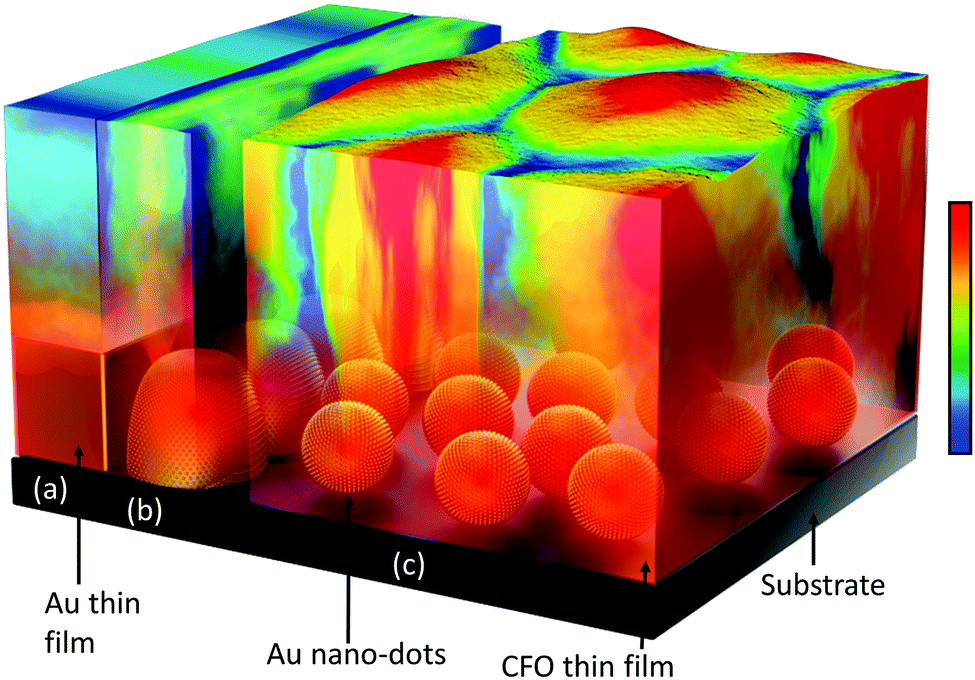 | ||
| Scheme 1 Schematic presenting the Au under-layer morphology-dependent crystallization behaviour of CFO: (a) CFO deposited on the Au continuous thin film is partially crystallized at the interface; (b) a larger Au island, which is an intermediate growth stage of Au dots to thin film, provides better crystallization compared to the continuous thin film; and (c) CFO is deposited on Au nano-dots, where the high surface area of Au interacts more proactively, leading to high room temperature crystallization by decreasing the free surface energy. The color scale denotes the degree of crystallization, where red and blue represent the maximum and minimum degrees of crystallization, respectively. | ||
Among the interesting potential metal under-layer candidates, Au (gold) is particularly attractive because of its remarkable manifold chemistry.10 Due to the relatively facile synthesis of Au nano-particles, they have various promising potential applications in solar cells,11 biosensors,12,13 reflective14 or antireflective coatings15 and, especially, in heterogeneous catalysis.16–18 Importantly, using Au as the catalyst metal leads to the lowest crystallization temperature compared to other metals.19 In general, sputter deposition plays a very important role in industrial and nanostructural processing20,21 and may be efficient and effective for the controlled production of Au nano-dots cluster surfaces; this motivated us to employ this method for the present work.
Room temperature nano-sized ferromagnets with switchable high magnetization in the form of thin film architectures have attracted widespread attention and broadened the scope of magnetic materials in the technology arena.22 Among magnetic oxides, inverse spinel cobalt ferrite, CoFe2O4(CFO), is one of the most industrially important members of the magnetic ferrite class; it is a uniquely useful material for magnetic spin filters,23 magneto-optical applications,24 spintronics devices, including strain-/charge-driven multiferroic nanostructures,25–27 magnetic recording media, and read/write heads.28 The magnetic anisotropy of CFO is highly sensitive to the synthesis conditions, Co![[thin space (1/6-em)]](https://www.rsc.org/images/entities/char_2009.gif) :Fe:O chemical ratio, cation occupancy of specific crystallographic sites and oxidation states. Most importantly, the synthesis temperature precisely governs the degree of crystallization, which is a deciding factor in tuning the properties not only of CFO but of almost all other systems as well. This directed us to use CFO as a ‘model’ system to demonstrate the effectiveness of Au nano-dots-induced room-temperature crystallization.
:Fe:O chemical ratio, cation occupancy of specific crystallographic sites and oxidation states. Most importantly, the synthesis temperature precisely governs the degree of crystallization, which is a deciding factor in tuning the properties not only of CFO but of almost all other systems as well. This directed us to use CFO as a ‘model’ system to demonstrate the effectiveness of Au nano-dots-induced room-temperature crystallization.
2. Results
The crystal structures of the Au nano-dots deposited at four different time frames (30, 60, 120 and 250 s) were recorded through X-ray diffraction (XRD). The average Au nano-dot/particle diameters were estimated to be 2.5 ± 0.5, ∼4 ± 1, 10 ± 2 and 20 ± 3 nm for the samples sputtered for 30, 60, 120 and 250 s, respectively (ESI,† Fig. S1). The Au nano-dots deposited for 120 and 250 s were confirmed to have fcc structures with preferred (111) orientations (ESI,† Fig. S1) (JCPDS No. 04-0784). The surface energies (γs) for the different planes of Au are γs(111) (790 ergs cm−2) < γs(100) (918 ergs cm−2) < γs(110) (980 ergs cm−2).29 The close-packed (111) plane possesses the lowest surface energy, followed by the (100) and (110) planes. Therefore, the (111) texture is favorable in Au fcc nano-dots due to surface energy minimization.It was difficult to observe the XRD peaks of Au deposited for 60 s due to the very small volume and size of Au. In terms of polycrystalline structures, the scattering volume is directly proportional to the integrated intensities of the Bragg reflections (I):
| Ihkl ∝ |Fhkl|2e−2M·LP·mhkl·V |
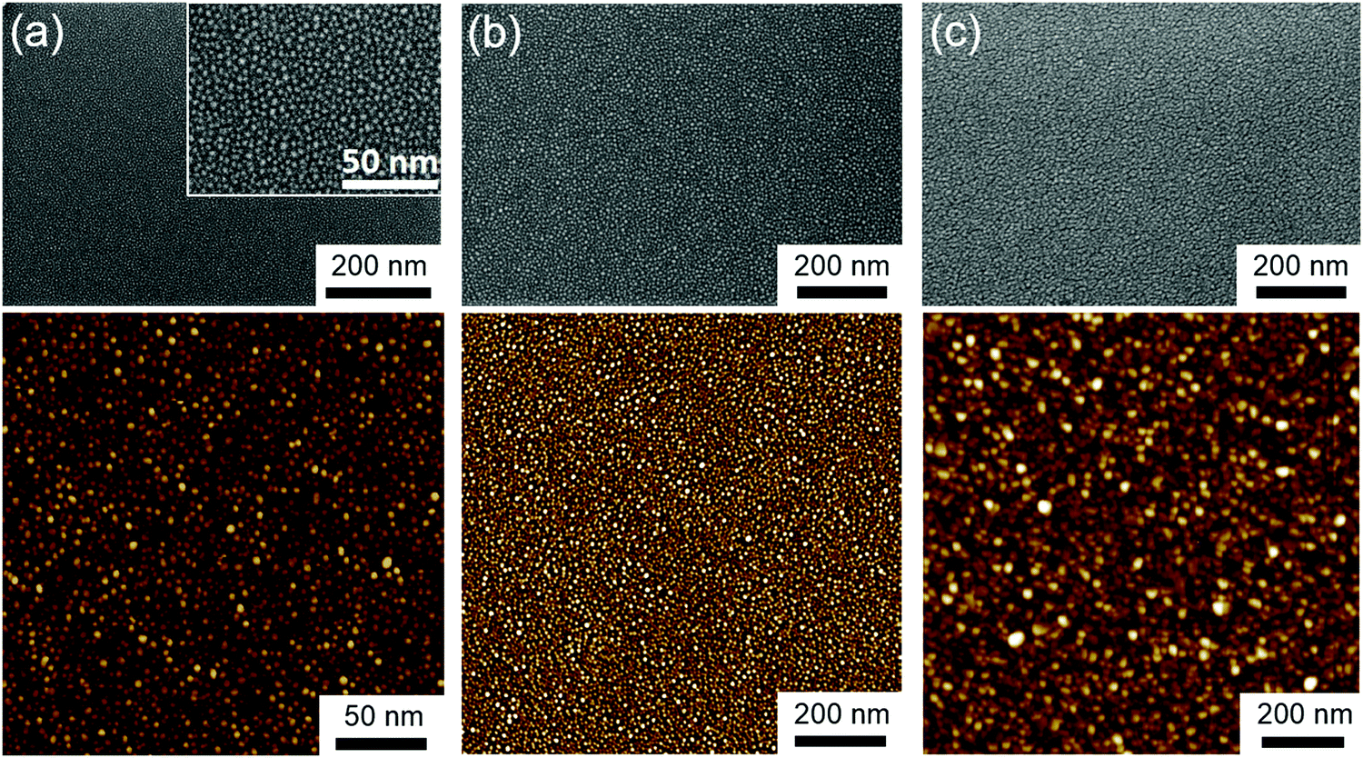 | ||
| Fig. 1 SEM (top) and AFM (bottom) images of the (a) 4 nm Au nano-dots, (b) 10 nm Au nano-dots and (c) 20 nm continuous Au thin film deposited by RF sputtering on SiO2/Si substrates for 60, 120 and 250 s, respectively. The inset of figure ‘a’ shows a high magnification SEM image of the 4 nm Au nano-dots. | ||
CFO thin films were deposited on the SiO2/Si substrate at room temperature with varying Au underlayer thicknesses; viz., (i) without Au underlayer, i.e. CFO monolayer, (ii) 4 nm Au nano-dots layer, (iii) 10 nm Au nano-dots layer and (iv) 20 nm Au underlayer. Fig. 2(c, d, g and h) shows XRD patterns of the CFO thin films deposited at room temperature with varying Au underlayer thicknesses. No traceable XRD peaks appeared in the CFO monolayer deposited without Au as an under-layer, indicating the amorphous nature of the thin film. Weak diffraction peaks were observed in the CFO (JCPDS No. 22-1086) deposited on the 10 and 20 nm Au nano-dots layers. The intensity of the CFO(311) peak remarkably increased when CFO was deposited on 4 nm Au nano-dots, confirming the increased crystallinity of the CFO thin film.
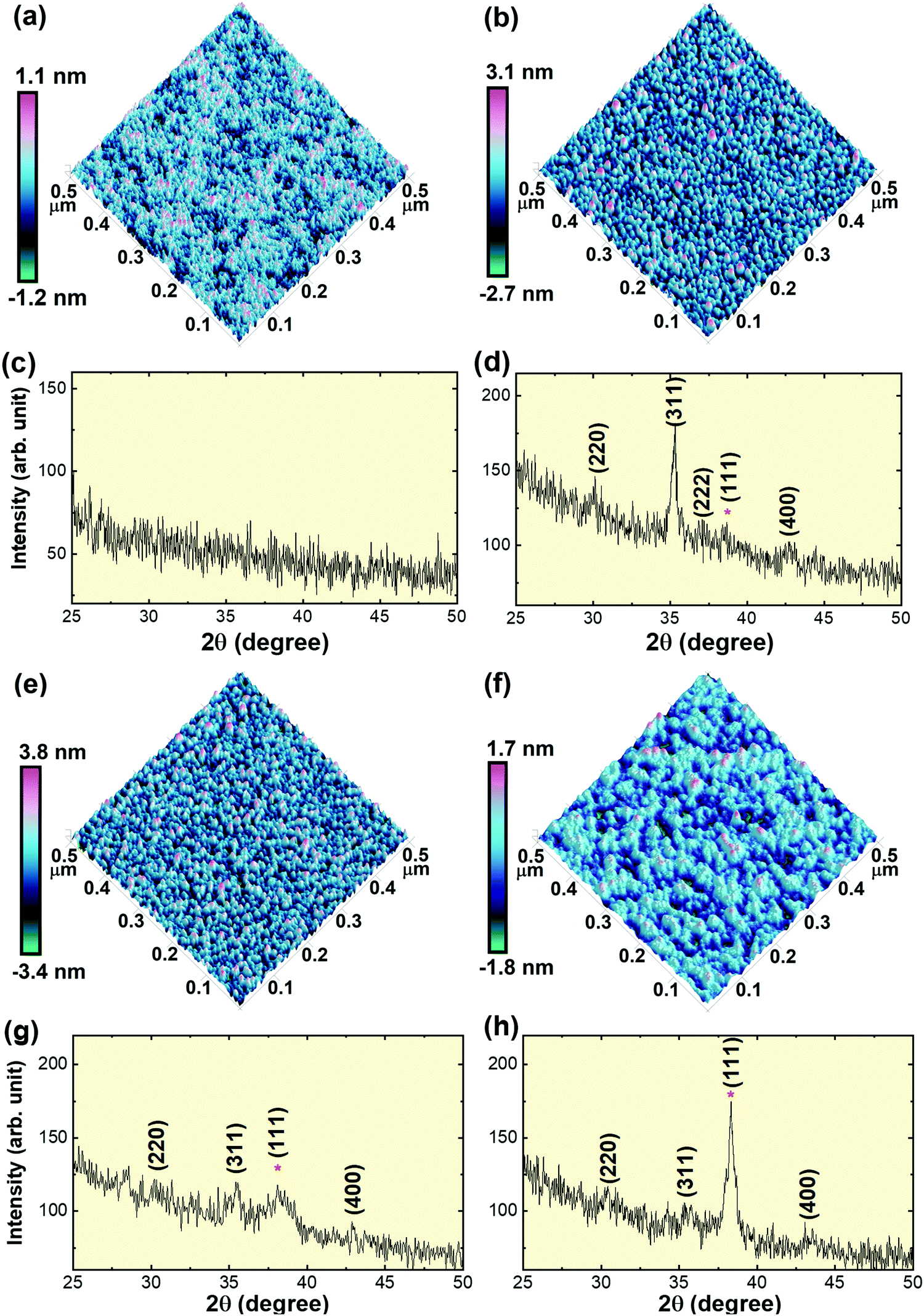 | ||
| Fig. 2 (a), (b), (e) and (f) AFM images of CFO thin films deposited at room temperature: (a) without an Au underlayer, (b) on 4 nm Au nano-dots, (e) on 10 nm Au nano-dots/layer and (f) on a 20 nm Au under-layer. (c), (d), (g) and (h) XRD patterns of CFO thin films deposited at room temperature; (c) without an Au underlayer, (d) on 4 nm Au nano-dots, (g) on 10 nm Au nano-dots/layer and (h) on a 20 nm Au under-layer. The intensity of the (311) peak is the highest in the randomly oriented CFO thin film deposited on 4 nm Au nano-dots, indicating enhancement of the CFO crystallization. Asterisks in the XRD patterns denote the (111) peak positions of Au. | ||
The out-of-plane lattice parameters (a⊥; c-axis) of CFO deposited on 4 and 10 nm Au nano-dots were calculated as 8.41 Å and 8.384 Å, respectively. The in-plane lattice parameter (a||; a-axis) of the CFO thin film deposited on 4 nm Au nano-dots was also determined and was found to be a|| = 8.415 Å. The calculated c/a (a⊥/a||) tetragonality ratio is 0.999. The a⊥ and a|| values of the CFO thin film on 4 nm Au are close to that of bulk CFO, and the negligible c/a ratio indicates film relaxation without a stress/strain mechanism. The (111) peaks of the Au nano-dots are marked by asterisks in the XRD patterns. The crystallite size (txrd) of the CFO thin film was calculated from the most intense (311) peak of the CFO thin film XRD patterns. The calculated txrd values are 7 (±2), 5 (±2) and 4 (±2) nm for the CFO thin films deposited on 4 nm Au nano-dots, 10 nm Au nano-dots and the 20 nm Au thin film, respectively.
The room temperature crystallization of the CFO thin films was also verified by AFM images (Fig. 2a, b, e and f). The surface morphology of the CFO thin film deposited on Au nano-dots is clearly distinct from that of the CFO monolayer. In the absence of an Au under-layer, an amorphous film was formed, while a well-defined crystalline surface morphology was achieved for CFO deposited on the 4 nm Au nano-dots array. The surface roughnesses obtained from the AFM images are 0.204, 0.629, 0.759 and 0.420 nm for CFO deposited without an Au underlayer and deposited on 4, 10 and 20 nm Au underlayers, respectively.
Cross-sectional TEM observations of the CFO thin film deposited on 4 nm Au nano-dots were carried out to determine the shapes and sizes of the Au nano-dots and the crystallization behaviour of the CFO thin film (Fig. 3a–e). Most of the Au nano-dots appeared to be uniform and spherical. The dark region shows the overlapping of Au nano-dots with each other; importantly, no Au nano-dots appear to be stacked on each other (Fig. 3a). This indicates that the arrangements of the Au nano-dots are 2-dimensional and not 3-dimensional. The crystal lattice planes observed in the image provide evidence of the crystallization of CFO. The HR-TEM image of the CFO deposited on Au nano-dots (Fig. 3b) shows well-defined crystallized lattice planes with a distance d ≈ 0.25 nm corresponding to the (311) plane of CFO, which is in good agreement with the XRD pattern. Fig. 3c shows a high magnification image of the Au nano-dots, and the corresponding line profile of the corresponding image of the Au nano-dots is shown in Fig. 3d. The observed distance of the lattice fringes is d ≈ 0.235 nm, revealing the presence of Au(111). The SAED pattern demonstrates that the Au nano-dots are in a polycrystalline state, where most of the Au is grown in the (111) direction. The ultra-small nature of the Au nano-dots is evidenced by the continuous (111) diffraction ring pattern associated with some bright intermediate spotty patterns (Fig. 3e). Ring patterns corresponding to (200) and (220) were also observed for the Au nano-dots. On the other hand, only a spotty dot pattern without a continuous ring corresponding to (311) and (440) was observed in the case of the CFO thin film, confirming the crystallization of CFO deposited on Au nano-dots. Cross-sectional TEM images of the CFO films deposited on the 2.5 and 10 nm Au underlayers are given in ESI,† Fig. S3a and b for the sake of comparison.
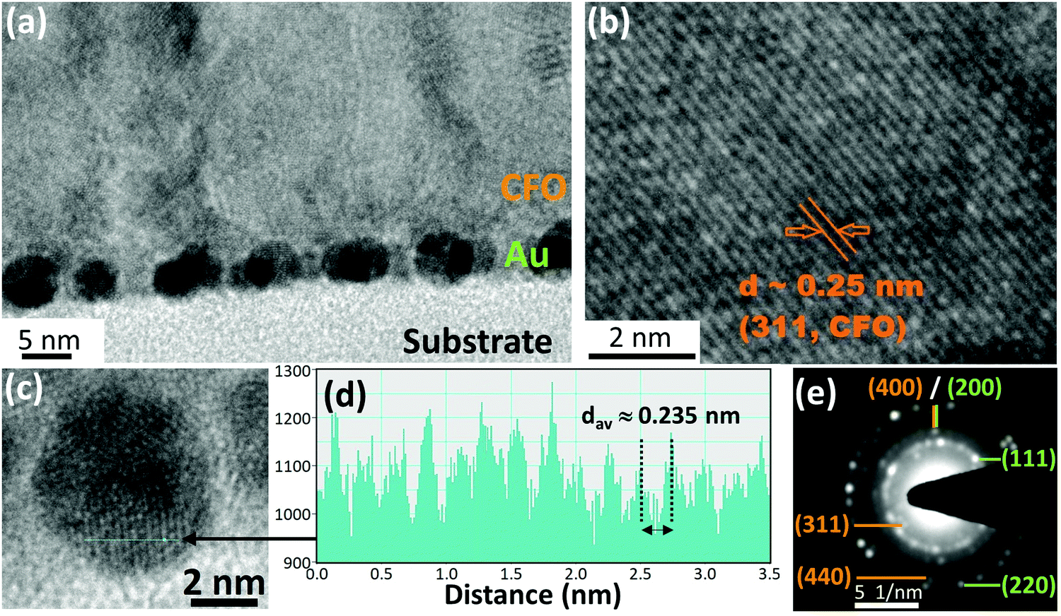 | ||
| Fig. 3 (a) CFO thin film deposited on 4 nm Au nano-dots; (b) HR-TEM image of CFO, where the observed interplanar spacing is 0.25 nm, corresponding to the (311) plane; (c) magnified HR-TEM image of an Au nano-dot; (d) line profile of the corresponding HR-TEM image of the Au nano-dot, where the lattice fringe (d ≈ 0.235 nm) is induced from the in-plane diffraction of Au along the (100) direction; (e) SAED pattern of CFO deposited on 4 nm Au. In the SAED pattern, orange and green notations correspond to the CFO and Au materials, respectively. | ||
The magnetization behavior of the CFO films was investigated to realize the effects of crystallization and the under-layer on the magnetic anisotropy. All the samples exhibited typical ‘S’-type M–H loops, which is a characteristic feature of ferrimagnetic CFO (Fig. 4a–c and ESI,† Fig. S3c and d). The magnetic parameters determined from these loops were remarkably varied by changing the underlayer conditions. The most important feature of the CFO films is their increased saturation magnetization (Ms) and coercivity (Hc) after deposition on 4 nm Au nano-dots. The Hc value measured in a perpendicular direction for CFO deposited on 4 nm Au nano-dots is almost 18-fold higher (Hc = 4150 ± 50 Oe) than that of the CFO monolayer film (Hc = 230 Oe). The Hc value is also around 4-fold higher than that of CFO deposited on the Au 10 nm thin film (Hc = 1067 Oe) and 8-fold higher than the coercivity of CFO deposited on the continuous Au thin film (Hc = 500 Oe). It is worth mentioning here that there is no lattice distortion in the CFO deposited on 4 nm Au nano-dots, and it is almost relaxed (as a = b ≈ c = 8.41 Å) in the thermo-equilibrium state without significant intrinsic strain. CFO is known to be highly magnetostrictive, with a positive first-order magneto-crystalline anisotropy constant (K1 ∼ 2 × 10⁶ ergs cc−1),34 which results in a high Hc. Therefore, the high Hc in the present case can be mainly attributed to the crystallinity rather than stress/strain mechanisms. However, shape anisotropy due to possible columnar growth of the CFO film or pinning of the magnetization at defects or grain boundaries may also contribute to the strong change in Hc. Considering the higher surface/interface of CFO with the Au nanodots, in particular, pinning of the magnetization would also tend to make a strongly enhanced contribution to Hc.
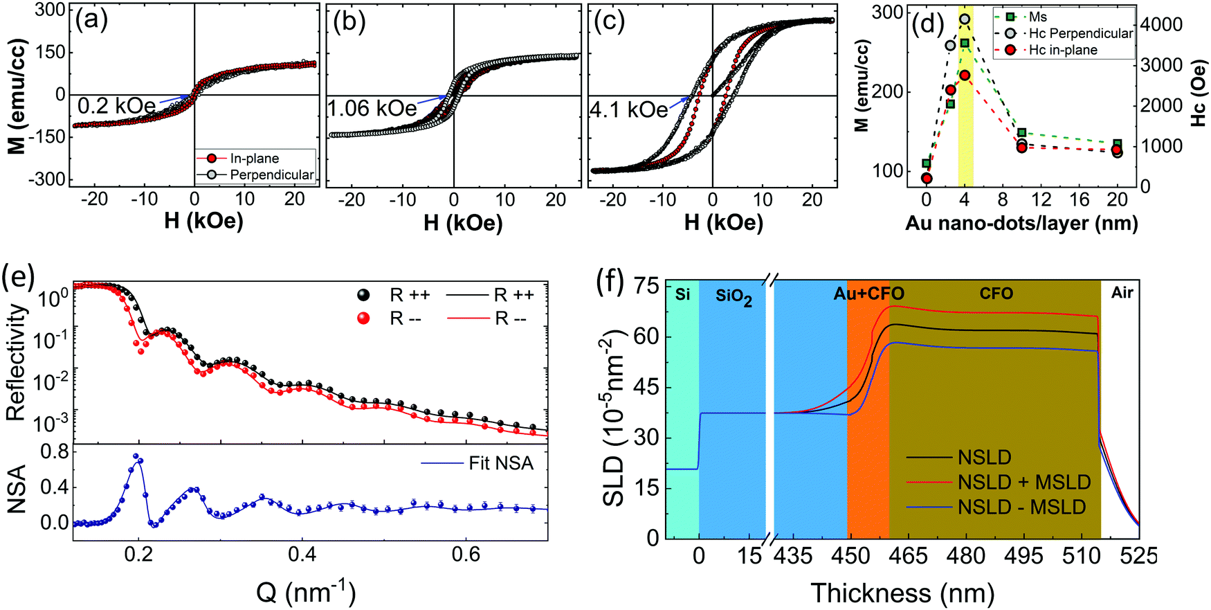 | ||
| Fig. 4 Magnetization (M) versus applied magnetic field (H) hysteresis loops measured at room temperature in the perpendicular and in-plane directions. M–H loops of CFO deposited (a) without an Au under-layer, (b) on the 10 nm thick Au under-layer and (c) on 4 nm Au nano-dots (the values inside the M–H loops show the observed coercivities in the perpendicular direction). (d) Observed magnetization parameters of CFO deposited on various under-layers. (e) and (f) PNR results of CFO deposited on 4 nm Au nano-dots: (e) the NSF reflectivity data sets (closed symbol) and best fits (solid line) and their corresponding NSA data sets and best fits; (f) the NSLD and MSLD models obtained from the best fit parameters. | ||
Similarly, Ms is 262 (±5) emu cc−1 for the CFO deposited on 4 nm Au nano-dots, which is almost two-and-a-half fold higher than the value of the CFO monolayer (Ms = 110 emu cc−1). The remnant magnetization (Mr) and squareness/remnant ratio (R = Mr/Ms) extracted from the M–H loops are given in ESI,† Fig. S3e. As with Ms, Mr also improved significantly for the CFO deposited on 4 nm Au nano-dots, giving rise to a better R value of 0.57. As is known, the magnetic anisotropies of magnetic films are mainly related to their degrees of crystallization. In magnetically soft nanocrystalline materials, the optimum magnetic anisotropy can be achieved even with a partially crystallized phase, i.e. dual-phase materials composed of an amorphous matrix with nanocrystals as inclusions. On the other hand, in magnetically hard materials such as CFO, almost full crystallization is required to render a large magnetic anisotropy. The observed Ms of CFO is still lower than that of the fully crystallized film, 380 emu cc−1,35 suggesting that the CFO thin film grown on 4 nm Au nano-dots is not fully crystallized. Post-annealing may be required for CFO deposited on 4 nm Au nano-dots to achieve maximum crystallization. Therefore, the CFO thin films deposited on 4 nm Au nano-dots were post-annaled at various temperatures and compared to our previous results of a fully crystallized CFO monolayer post-annealed at 800 °C for 4 h.34 Interestingly, crystallization of the CFO thin films deposited on Au nano-dots was achieved at a significantly lower annealing temperature (250 °C) and shorter time (2 h) than our previously reported reuslts. The crystallization was achieved at a nearly 550 °C lower temperature and in 2 h less time than that of the CFO monolayer deposited without an Au under-layer. Therefore, this approach of using Au nano-dots as an under-layer has significant advantages of decreased annealing temperature and time.
In order to support the magnetization data and the higher crystallizaiton behaviour observed at the Au/CFO interface, we carried out polarised-neutron reflectometry (PNR) experiments due to the high depth resolution of this technique in thin film samples and, more importantly, its ability to detect magnetic signals throughout the thickness of the samples (ESI,†). To obtain the magnetic depth profile of the CFO thin film deposited on 4 nm Au nano-dots, measurements of R++ and R−− were performed at ambient temperature (300 K) with an applied magnetic field of 10 kOe, as shown in Fig. 4(e and f), where Fig. 4(e) shows the non-spin-flip (NSF) reflectivity and neutron spin asymmetry (NSA) results calculated by NSA = (R++ − R−−)/(R++ + R−−). The R++ and R−− reflectivity data show typical results for a single magnetic layer grown on a substrate with a reasonably flat film surface. Through careful data analysis, the PNR results corroborate that the Au nano-dots facilitate room temperature crystallization of CFO. A PNR experiment was also carried out on the 4 nm Au nano-dots in order to obtain the magnetization contribution from the Au nano-dots. No profound magnetic contribution from the 4 nm Au nano-dots was observed (ESI,† Fig. S4).
The nature of chemical bonding at the interface and the promotion of crystal growth by the interface chemistry were examined through DFT calculations. Four CFO(311) surface terminations were examined theoretically when constructing the interface (ESI,† Fig. S5). The most stable configuration was used for analyzing the bonding characteristics at the interface. Fig. 5(a) shows the fully relaxed CoFe2O4(311) surface. Similar to many oxides, the surface is more stable when terminated with bridging O atoms.36 The interaction between the CoFe2O4(311) surface and Au(111) surface at the interface, however, causes a significant surface reconstruction, which is shown in Fig. 5(b). This reconstruction manifests as the depression of O ions away from the outermost layer of the interface into the inner layers of CoFe2O4. The depressed O atoms are marked with red arrows in Fig. 5(a). Consequently, the average Fe–Au and Co–Au bond lengths at the interface, being both 2.73 Å, are shorter than that of the Fe–O bond, which is 2.82 Å. We therefore anticipated that the Au atoms would have a stronger tendency to bond with Fe and Co atoms than with O atoms. This tendency was further confirmed by the COHP analysis of the shortest Fe–Au, Co–Au and O–Au bonds (marked with dotted lines in Fig. 5(b)) presented in Fig. 5(c)–(e). Negative –COHP values indicate antibonding states, while positive –COHP values indicate bonding states. The bonding states for all the bonds are located in the region between −8 and −4 eV from the Fermi level. The antibonding states, on the other hand, dominate the immediate region below the Fermi level. As marked with an orange arrow in Fig. 5(e), the O–Au bond has relatively large antibonding states compared to the Fe–Au and Co–Au bonds, which destabilises the Au–O bond. The integrated –COHP (–ICOHP) values, which are an indicator of bond strength, are 0.6278 eV per bond, 0.6661 eV per bond and 0.3429 eV per bond for the marked Fe–Au, Co–Au and O–Au bonds, respectively, demonstrating the affinity of Au for bonding with Fe and Co at the interface.
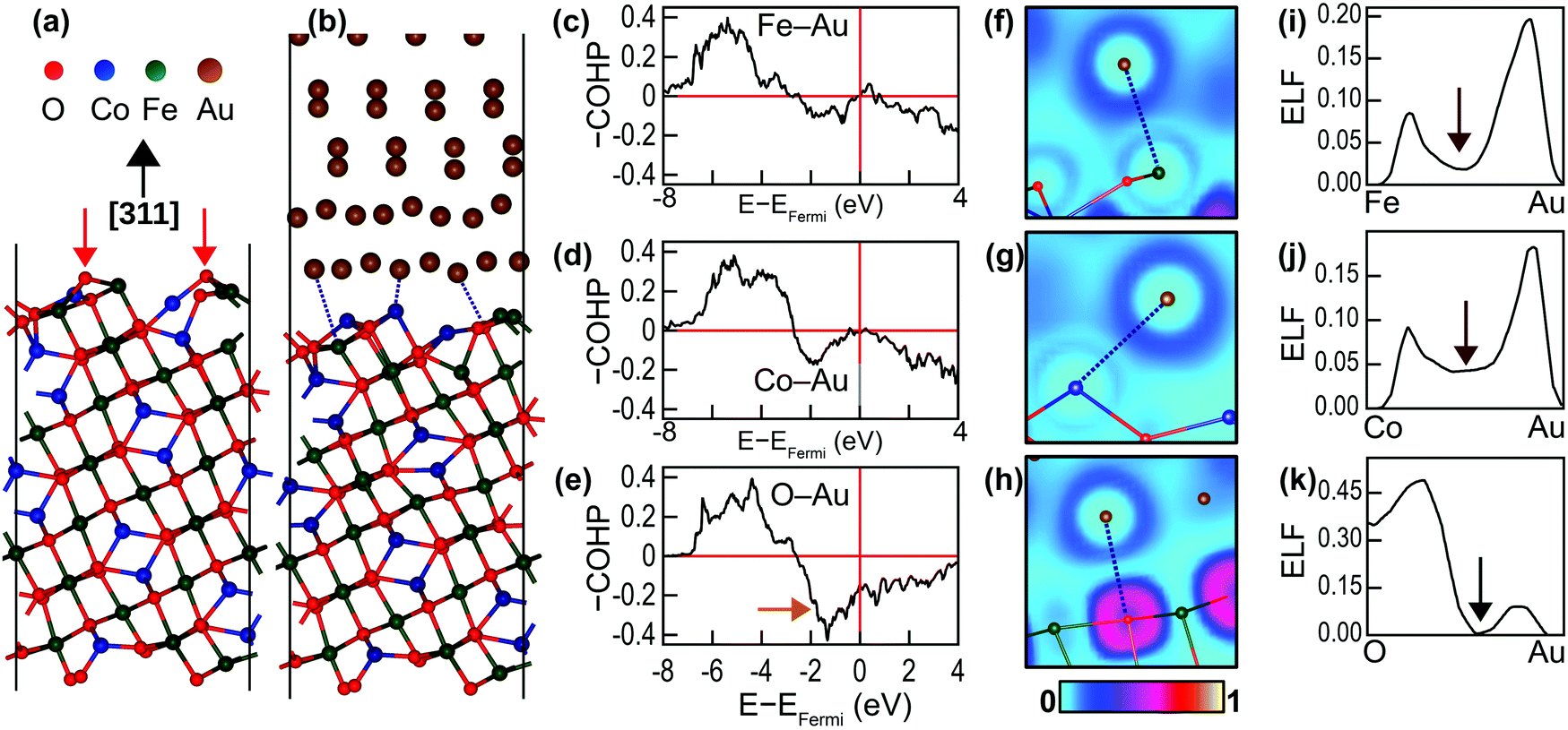 | ||
| Fig. 5 Schematics of (a) the fully relaxed CoFe2O4(311) surface and (b) the CoFe2O4(311)/Au(111) interface. The dotted lines in (b) mark the shortest Fe–Au, Co–Au and O–Au bonds in the supercell. The negative values of the crystal orbital Hamilton populations (–COHP) for those bonds are presented in (c), (d) and (e), respectively. The electronic localisation functions (ELF) in the planes containing the marked (f) Fe–Au, (g) Co–Au and (h) Au–O bonds. (i), (j) and (k) show the line profiles of ELF of the bonds presented in (f), (g) and (h), respectively. | ||
The nature of the bonds at the interface can be identified by examining the electronic localisation function (ELF), which is defined as the likelihood of finding a second spin-like electron at a given point. Fig. 5(f)–(h) depicts the ELF field around the bonding atoms, while Fig. 5(i)–(k) presents the line profiles of ELF along the bonds. For the Fe–Au and Co–Au bonds, the ELF values vanish to zero at the metal centres and peak in the inter-atomic region. Moreover, the ELF values never drop to zero in the mid-bond region (marked with brown arrows in Fig. 5(i) and (j)). This EFL profile indicates metallic bonding. The ELF profile for O–Au, on the other hand, is quite different. The ELF value at the O site is 0.3571, and it further peaks near the O site to 0.4998 and decreases to zero at the mid-bond (marked with a green arrow in Fig. 5(k)). This ELF profile corresponds to ionic bonding. However, because the maximum ELF value along the bond is ∼0.5, the ionicity of this bond is rather weak (the maximum ELF in strong ionic bonds approaches one).
3. Discussion
The growth mechanism of Au nano-dot arrays into continuous thin films is a step-wise process that occurs through (a) nucleation, (b) lateral growth, (c) coalescence and (d) vertical growth (Fig. 6). Au atoms are adsorbed and diffuse along the surface after impinging on the SiO2/Si substrate by dissipating their kinetic energy. The chemical bonds and interactions between amorphous SiO2 and Au are very weak, resulting in desorption of the Au adatoms. The process of formation of stable dimers can be initialized, and these can serve as condensation nuclei. Triple atom collision stabilizes these dimers by conserving energy and momentum.26 Two or more adatoms join together to form stable nuclei; these newly formed stable nuclei then adsorb a few more new diffusing adatoms, resulting in the growth of a small cluster. The driving force behind the formation of Au small cluster growth may be the so-called “aurophilicity,”, where the inter- and intra-molecular interactions are based on dispersive effects among the 5d10-shells of adjacent Au atoms.37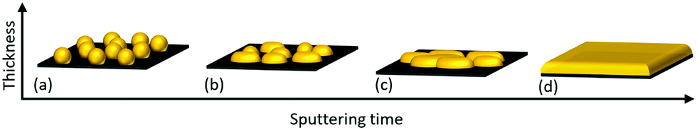 | ||
| Fig. 6 Transformation of Au nano-dots to thin film at different growth stages: (a) nucleation, (b) lateral growth, (c) coalescence and (d) vertical growth. | ||
The amorphous nature of SiO2 provides no crystal-lattice plane to Au, and the non-wetting behaviour of Au on SiO2 tends to minimize the surface area of Au clusters on the SiO2 interface, leading to the formation of hemispherical shapes through the Vomer-Weber mode.38,39 This agglomeration of Au clusters and their transformation to hemisphere islands decreases the total free energy with the interface. These Au hemisphere islands are treated by rapid post-annealing so that atomic diffusion occurs, leading to their transformation to spherically shaped Au nano-dots by further decreasing their free energy (Fig. 6a). The nucleation process continues until a critical Au cluster density is formed; this increases the probability of diffusion of impinging adatoms into existing Au clusters, thereby decreasing the probability of formation of new stable nuclei.
The self-amplified lateral growth of Au clusters is dominant over vertical growth in the second stage of the growth process (Fig. 6b), where the mean free path of diffusing adatoms is decreased, leading to an increase in their condensation probability on the Au cluster-covered substrate surface.40 If the cluster size is small enough, the clusters can travel along the surface and approach other clusters.41 At a point where two clusters come close to each other, they tend to fuse together, resulting in permanent diffusion-driven coalescence by decreasing the surface free energy and, henceforth, increasing the growth rate (Fig. 6c). This process is similar to post-deposition Smoluchowski ripening.42 With a further increase in Au deposition time, the cluster size increases, which limits the cluster mobility. The adsorption of freely moving atoms by the clusters leads to adsorption-driven cluster growth.43 At a certain film thickness, the mean cluster diameter exceeds the correlation distance and covers most of the substrate area; adsorptive growth proceeds further only in the vertical direction (Fig. 6d).
It can be observed from Fig. 2(d and g) that the Bragg reflections from the (311) peak are more pronounced in CFO than the weakly contributing (220) and (400) reflections. Au as an under-layer is oriented in the (111) direction, and the γs values for different planes of CFO are anisotropic, where γs(111) (208 ergs cm−2) < γs(400) (1486 ergs cm−2) < γs(220) (1916 ergs cm−2) < γs(311) (2344 ergs cm−2);19 therefore, CFO deposited on Au is expected to grow in the (111) direction. However, it is worth mentioning here that the (111) reflection from CFO at ∼20° is hardly noticeable (therefore, the XRD pattern below 25° is not shown in Fig. 2). Apart from the γs minimizing effect, the elastic strain energy density (Mhklε2) also influences the total energy and the film orientation. Mhklε2 depends on the crystallographic orientations (hkl) and the effective Mhkl of the grains.34,44Mhkl can be calculated as a function of the grain orientation (hkl) and the stiffness constants (C11, C12 and C44) as Mhkl = C11 + C12 + K − [2(C12 − K)2/(C12 + 2K)], where K = (2C44 − C11 + C12)(h2k2 + k2l2 + h2l2)/(h2 + k2 + l2).44 The CFO thin film deposited on Au should have the values of Mhklε2, Mhkl(111) (3.68 × 10¹² dynes per cm2) > Mhkl(311) (3.09 × 10¹² dynes per cm2).45 This reveals that CFO(311) possesses a smaller strain energy density than CFO(111), leading to a random orientation of the CFO thin film rather than an orientation in the (111) direction.
On the basis of our results, the CFO thin film deposited at room temperature on a 4 nm-sized Au nano-dots array is highly crystallized, which also demonstrates enhanced magnetic anisotropies. The TEM results suggest that there is a crystallization gradient in the out-of-plane direction which is responsible for the magnetization gradient in the CFO in a vertical direction to the plane of the substrate. The PNR experiments were helpful to support our claims and to analyse the magnetization gradients. The PNR fitting model given in Fig. 4e for nuclear scattering length density (NSLD) is consistent with the cross-section TEM results, where a gradual decrease of NSLD was observed from the Au nano-dot/CFO interface to the film surface pependicular to the substrate. Correspondingly, higher magnetization was achieved at the CFO/Au nano-dot interface, and the magnetization decreased gradually with the NSLD. The fitting model consists of a quadruple-layer structure: Si (substrate)/SiO2 (450 nm)/Au-CFO (5.5 nm)/CFO (59.5 nm). The NSLD of the CFO layer gradually decreased from the Au-CFO layer to the film surface. The average magnetisation determined from magnetic-SLD (MSLD) was in good agreement with the magnetisation data obtained from VSM.
In general, it is known that crystallization starts from a relatively slow nucleation step and is related to the nature of the metal underlayer.46–50 According to the DFT calculations, the Au surface attracts the atomic species through metallic bonding. This appears to be the first chemical reaction during the growth process. After a metallic Fe–Co monolayer has been formed on the Au nano-dot surface, O atoms bond to the Fe and Co centres and further facilitate the growth of CoFe2O4. One critical condition for the formation of the first metallic monolayer at the interface is that the Fe–Au and Co–Au bonds must be stronger than the Au–O bonds at the interface; this is the case here, as demonstrated in Fig. 5(c)–(e). The formation of more malleable metallic bonds at the Au/CFO interface provides the atomic flexibility at the interface that is required for the initial nucleation prior to the crystallization process. Furthermore, because the Au nano-dots offer a larger Au surface area (versus the continuous Au film) that attracts more Fe and Co species, there will be a greater number of possible CFO nucleation sites, which in turn promotes the CFO crystallization.
In our case, the crystallization of CFO is highly dependent on the morphology of the Au nano-dots which are serving as the under-layer (Scheme 1). As illustrated in Scheme 1c and Fig. 3, the Au nano-dots as a metal under-layer provide a higher surface area to interact with upper-layer CFO than a continuous Au thin film or fused Au particles with larger sizes (Scheme 1a and b). Moreover, the acceleration of CFO crystallization on the Au nano-dots can be attributed to the following facts: (i) Au crystallized in the preferred (111) direction, which exposes the lowest surface free energy to CFO (as evident from the TEM and SAED patterns, Fig. 3c–e); (ii) the Au nano-dots have surprisingly high catalytic activities, in marked contrast to their high ionization potential (9.23 V) in the bulk form (here, the continuous thin film can be treated as bulk), which is a poor catalyst; and (iii) the Gibbs surface free energy is minimized in the spherical Au nano-dots compared to the continuous thin film. Au nano-dots-induced crystallization caused crystallographic changes in the CFO through a decrease in the total anisotropy energy, E = Mhklε2 + [(γi + γs)/h], where Mhklε2 is the elastic strain energy density, γi and γs are the interfacial and surface energies, respectively, and h is the film thickness.34
The initial nucleation sites at the triple point grain boundaries at the CFO–Au interface also diffuse CFO to the already crystallized area from the amorphous area because the critical nucleation energy in the triple point grain boundary sites is relatively low compared to that of the flat surface.6 This resulted in a decrease of the free energy of the CFO material during the transformation of the amorphous phase to the crystalline phase; this rearrangement took place at the atomic level, which would provide the driving force for MIC. In other words, it can be considered as an interstitial metal diffusion-induced decrease in the activation energy of metal dissociation.51 Electronic screening of the covalent bonding in the CFO materials while in contact with the Au nano-dots could also occur according to Hiraki's screening model.6,52 After close observations of the CFO growth via TEM, we observed that CFO tends to grow in a columnar fashion. The assumptions related to the vertical growth of CFO are also well-supported by the PNR results. The possible mechanism for the vertical columnar growth of crystalline CFO is described in the ESI.†
4. Conclusions
In this work, for the first time, an innovative but simple approach is proposed to achieve room temperature metal-induced crystallization of thin films and to manipulate their crystallinity. In this context, an array of 4 nm-sized Au nano-dots with a uniform spatial distribution was deposited on an amorphous SiO2/Si substrate by RF magnetron sputtering. These nano-dots offer a high surface area and minimize the surface freee energy at the interface, leading to metal-induced room temperature crystallization in the CFO upper-layer thin film. The crystallization in CFO was confirmed through XRD, TEM and AFM techniques. Moreover, improved magnetic anisotropy of the CFO was also demonstrated by an 18-fold increase in the coercivity and an 4-fold increase in the saturation magnetization. This novel approach is greatly advantageous over conventional post-annealing methods not only to decrease the annealing temperature and time but also to preserve the chemical composition, structure and smooth surface of the functional material. This will also afford enormous opportunities for the low-cost room temperature growth of many other oxides and even metal thin films.5. Experimental section
Preparation of Au nano-dot arrays
Au nano-dots were deposited on thermally oxidized Si substrates (SiO2/Si) by an RF–magnetron-sputtering system. Initially, the vacuum chamber was evacuated to a pressure of 0.5 × 10⁻⁶ Torr; then, Ar was introduced up to a pressure level of 2.0 × 10⁻³ Torr to perform Au sputtering for 30, 60, 120 and 250 s at 100 °C while maintaining a deposition power of 10 W. The sputtering power density was 0.49 W cm−2 in this study.Deposition of the CoFe2O4 thin film at room temperature
60 nm thin films of CoFe2O4 (CFO) were grown on Au nano-dot arrays by DC sputtering via the facing target sputtering technique at room temperature. A CoFe2O4 ceramic target supplied by Kojyundo Chemical Laboratory Co., LTD was utilized for the CFO thin film deposition. The CFO sputtering was carried out by applying a DC power of 30 W and maintaining an Ar atmosphere at 0.4 Pa.Characterizations
X-ray diffraction (Rigaku SmartLab), atomic/magnetic force microscopy (Veeco, Innova), vibrating sample magnetometry (Tamagawa Factory Co. Ltd, Japan), field-emission scanning electron microscopy (Hitachi SU8000) and transmission electron microscopy (Philips CM12) were used to study the crystallization behavior of the CFO thin films on Au nano-dots. Polarized neutron reflectometry (PNR) experiments were carried out using the time-of-flight PLATYPUS polarised neutron reflectometer located at the Australian Nuclear Science and Technology Organisation (ANSTO), Sydney, Australia.53 Details of the PNR measurements are given in the ESI.† To obtain the magnetic depth profiles of the three samples, the measurements of R++ and R−− (non-spin-flip reflectivity channels) were performed at ambient temperature (or 300 K) with an applied magnetic field of 1 T.DFT calculations
Spin-polarized density functional calculations were carried out using VASP code54 with a generalized gradient approximation and projector augmented wave pseudopotentials55 with a cut-off energy of 550 eV. Lobster code was used to analyze the crystal orbital Hamilton population (COHP) at the interface.56 For Fe and Co ions, Hubbard terms57 of Ueff = 5.3 eV and 3.3 eV were adopted as stipulated in Materials Project.58 The surfaces were cleaved from fully optimized CFO and Au lattices. The differences between the calculated bulk lattice parameters and the experimental values were negligible. The interface was constructed by stacking two conventional unit-formulas of CFO cleaved in the (311) direction amounting to a Co16Fe32O64 supercell. On top of the optimized CFO surface, a 4u × 2v Au(111) surface of nine atomic Au layers was added. A vacuum slab of 20 Å was also added to the supercell. Atoms located at the three outermost atomic layers away from the interface were fixed to their positions, while all other atoms closer to the interface were allowed to relax.Conflicts of interest
The authors declare no conflict of interest.Acknowledgements
One of the authors (SES) is very thankful to the Japan Society for the Promotion of Science for providing the financial support (Grant-in-Aid) for scientific research. The computational resources were provided by the Integrated Materials Design Centre at the University of New South Wales, Sydney, Australia. The authors are thankful to ANSTO for providing PNR measurements through proposal no. 6670 (2018). This work was also supported by the Australian Research Council (ARC) Future Fellow (grant FT150100479). This work was performed in part at the Queensland node of the Australian National Fabrication Facility, a company established under the National Collaborative Research Infrastructure Strategy to provide nano and micro-fabrication facilities for Australia's researchers.References
- J. Su, X. Zou, B. Li, H. Chen, X. Li, Q. Yu, Q. Mi and J.-S. Chen, Accelerated room-temperature crystallization of ultrahigh-surface-area porous anatase titania by storing photogenerated electrons, Chem. Commun., 2017, 53, 1619–1621 RSC.
- F. Cheng, J. Shen, B. Peng, Y. Pan, Z. Tao and J. Chen, Rapid room-temperature synthesis of nanocrystalline spinels as oxygen reduction and evolution electrocatalysts, Nat. Chem., 2011, 3, 79–84 CrossRef CAS PubMed.
- Z. Li, J. Du, Q. Tang, F. Wang, J.-B. Xu, J. C. Yu and Q. Miao, Induced crystallization of rubrene in thin-film transistors, Adv. Mater., 2010, 22, 3242–3246 CrossRef CAS PubMed.
- K. A. John, M. Thankamoniamma, J. Puigdollers, R. Anuroop, B. Pradeep, T. Shripathi and R. R. Philip, Rapid room temperature crystallization of TiO2 nanotubes, CrystEngComm, 2017, 19, 1585–1589 RSC.
- Z.-K. Wang, X. Gong, M. Li, Y. Hu, J.-M. Wang, H. Ma and L.-S. Liao, Induced crystallization of perovskites by a perylene underlayer for high-performance solar cells, ACS Nano, 2016, 10, 5479–5489 CrossRef CAS PubMed.
- Q. Li, C. Chen, Z. Chen, Z. Jiao, M. Wu, C.-H. Shek, C. M. Lawrence Wu and J. K. L. Lai, Al-Induced crystallization of amorphous Ge and formation of fractal Ge micro-/nanoclusters, Inorg. Chem., 2012, 51, 8473–8478 CrossRef CAS PubMed.
- L. Li, H. Tissot, S. Shaikhutdinov and H.-J. Freund, Transition metal induced crystallization of ultrathin silica films, Chem. Mater., 2017, 29, 931–934 CrossRef CAS.
- F. Qu, C. Li, Z. Wang, H. P. Strunk and J. Maier, Metal-induced crystallization of highly corrugated silicon thick films as potential anodes for Li-ion batteries, ACS Appl. Mater. Interfaces, 2014, 6, 8782–8788 CrossRef CAS PubMed.
- O. Nast and A. J. Hartmann, Influence of interface and Al structure on layer exchange during aluminum-induced crystallization of amorphous silicon, J. Appl. Phys., 2000, 88, 716–724 CrossRef CAS.
- S. A. Claridge, A. W. Castleman Jr., S. N. Khanna, C. B. Murray, A. Sen and P. S. Weiss, Cluster-assembled materials, ACS Nano, 2009, 3, 244–255 CrossRef CAS PubMed.
- B. Paci, A. Generosi, V. R. Albertini, G. D. Spyropoulos, E. Stratakis and E. Kymakis, Enhancement of photo/thermal stability of organic bulk heterojunction photovoltaic devices via gold nanoparticles doping of the active layer, Nanoscale, 2012, 4, 7452–7459 RSC.
- H. Hiep, H. Yoshikawa, M. Saito and E. Tamiya, An Interference localized surface plasmon resonance biosensor based on the photonic structure of Au nanoparticles and SiO2/Si multilayers, ACS Nano, 2009, 3, 446–452 CrossRef CAS PubMed.
- J. Xu, L. Zhang, H. Gong, J. Homola and Q. Yu, Tailoring plasmonic nanostructures for optimal SERS sensing of small molecules and large microorganisms, Small, 2011, 7, 371–376 CrossRef CAS PubMed.
- M. Wolkenhauer, G.-G. Bumbu, Y. Cheng, S. V. Roth and J. S. Gutmann, Investigation of micromechanical cantilever sensors with microfocus grazing incidence small-angle X-ray scattering, Appl. Phys. Lett., 2006, 89, 054101 CrossRef.
- B. Gompf, J. Beister, T. Brandt, J. Paum and M. Dressel, Nanometer-thick Au-films as antireflection coating for infrared light, Opt. Lett., 2007, 32, 1578–1580 CrossRef CAS PubMed.
- M. Valden, X. Lai and D. W. Goodman, Onset of catalytic activity of gold clusters on titania with the appearance of nonmetallic properties, Science, 1998, 281, 1647–1650 CrossRef CAS PubMed.
- G. Li, H. Qian and R. Jin, Nanoscale, 2012, 4, 6714 RSC.
- I. Green, W. Tang, M. Neurock and J. Yates, Spectroscopic observation of dual catalytic sites during oxidation of CO on a Au/TiO2 catalyst, Science, 2011, 333, 736–739 CrossRef CAS PubMed.
- W. Knaepen, S. Gaudet, C. Detavernier, R. L. V. Meirhaeghe, J. J. Sweet and C. Lavoie, In situ X-ray diffraction study of metal induced crystallization of amorphous germanium, J. Appl. Phys., 2009, 105, 83532–83537 CrossRef.
- F. Faupel, V. Zaporojtchenko, T. Strunskus and M. Elbahri, Metal-polymer nanocomposites for functional applications, Adv. Eng. Mater., 2010, 12, 1177–1190 CrossRef CAS.
- M. Schwartzkopf, A. Buffet, V. Korstgens, E. Metwalli, K. Schlage, G. Benecke, J. Perlich, M. Rawolle, A. Rothkirch, B. Heidmann, G. Herzog, P. Muller- Buschbaum, R. Rohlsberger, R. Gehrke, N. Stribeck and S. V. Roth, From atoms to layers: in situ gold cluster growth kinetics during sputter deposition, Nanoscale, 2013, 5, 5053–5062 RSC.
- T. E. Quickel, V. H. Le, T. Brezesinski and S. H. Tolbert, On the correlation between nanoscale structure and magnetic properties in ordered mesoporous cobalt ferrite (CoFe2O4) thin films, Nano Lett., 2010, 10, 2982–2988 CrossRef CAS PubMed.
- A. V. Ramos, T. S. Santos, G. X. Miao, M.-J. Guittet, J.-B. Moussy and J. S. Moodera., Influence of oxidation on the spin-filtering properties of CoFe2O4 and the resultant spin polarization, Phys. Rev. B: Condens. Matter Mater. Phys., 2008, 78, 180402 CrossRef.
- D. Erdem, N. S. Bingham, F. J. Heiligtag, N. Pilet, P. Warnicke, L. J. Heyderman and M. Niederberger, CoFe2O4 and CoFe2O4-SiO2 nanoparticle thin films with perpendicular magnetic anisotropy for magnetic and magneto-optical applications, Adv. Funct. Mater., 2016, 26, 1954–1963 CrossRef CAS.
- H. Zheng, J. Wang, S. E. Lofland, Z. Ma, L. Mohaddes-Ardabili, T. Zhao, L. Salamanca-Riba, S. R. Shinde, S. B. Ogale, F. Bai, D. Viehland, Y. Jia, D. G. Schlom, M. Wuttig, A. Roytburd and R. Ramesh, Multiferroic BaTiO3-CoFe2O4 nanostructures, Science, 2004, 303, 661–663 CrossRef CAS PubMed.
- F. Zavaliche, H. Zheng, L. Mohaddes-Ardabili, S. Y. Yang, Q. Zhan, P. Shafer, E. Reilly, R. Chopdekar, Y. Jia, P. Wright, D. G. Schlom, Y. Suzuki and R. Ramesh, Electric field-induced magnetization switching in epitaxial columnar nanostructures, Nano Lett., 2005, 5, 1793–1796 CrossRef CAS PubMed.
- C. A. F. Vaz, J. Hoffman, C. H. Anh and R. Ramesh, Magnetoelectric coupling effects in multiferroic complex oxide composite structures, Adv. Mater., 2010, 22, 2900–2918 CrossRef CAS PubMed.
- Q. Dai, D. Berman, K. Virwani, J. Frommer, P.-O. Jubert, M. Lam, T. Topuria, W. Imaino and A. Nelson, Self-assembled ferrimagnet-polymer composites for magnetic recording media, Nano Lett., 2010, 10, 3216–3221 CrossRef CAS PubMed.
- S. M. Foiles, M. I. Baskes and M. S. Daw, Embedded-atom-method functions for the fcc metals Cu, Ag, Au, Ni, Pd, Pt, and their alloys, Phys. Rev. B: Condens. Matter Mater. Phys., 1986, 33, 79837991 CrossRef.
- I. M. Lifsitz and V. V. Slyozov, The kinetics of precipitation from supersaturated solid solutions, J. Phys. Chem. Solids, 1961, 19, 35–50 CrossRef.
- B. K. Chakraverty, Grain size distribution in thin films − 1. Conservative systems, J. Phys. Chem. Solids, 1967, 28, 2401–2412 CrossRef CAS.
- M. Z. Allmang, L. C. Feldman and M. H. Grabow, Clustering on surfaces, Surf. Sci. Rep., 1992, 16, 377–463 CrossRef.
- F. Ruffino, M. G. Grimaldi, C. Bongiorno, F. Giannazzo, F. Roccaforte and V. Raineri, Microstructure of Au nanoclusters formed in and on SiO2, Superlattices Microstruct., 2008, 44, 588 CrossRef CAS.
- S. E. Shirsath, X. Liu, Y. Yasukawa, S. Li and A. Morisako, Switching of magnetic easy-axis using crystal orientation for large perpendicular coercivity in CoFe2O4 thin film, Sci. Rep., 2016, 6, 30074 CrossRef CAS PubMed.
- M. Coll, J. M. Montero Moreno, J. Gazquez, K. Nielsch, X. Obradors and T. Puig, Low temperature stabilization of nanoscale epitaxial spinel ferrite thin films by atomic layer deposition, Adv. Funct. Mater., 2014, 24, 5368–5374 CrossRef CAS.
- M. Sterrer and H. Freund, Properties of Oxide Surfaces, in Surface and Interface Science, ed. K. Wandelt, 2014, DOI:10.1002/9783527680559.ch15.
- P. Pyykko, Theoretical chemistry of gold, Angew. Chem., Int. Ed., 2004, 43, 4412–4456 CrossRef PubMed.
- B. Ressel, K. C. Prince, S. Heun and Y. Homma, Wetting of Si surfaces by Au–Si liquid alloys, J. Appl. Phys., 2003, 93, 3886–3892 CrossRef CAS.
- Y. Han, D. S. He, Y. Liu, S. Xie, T. Tsukuda and Z. Y. Li, Size and shape of nanoclusters: single-shot imaging approach, Small, 2012, 8, 2361–2364 CrossRef CAS PubMed.
- V. Zaporojtchenko, K. Behnke, A. Thran, T. Strunskus and F. Faupel, Condensation coefficients and initial stages of growth for noble metals deposited onto chemically different polymer surfaces, Appl. Surf. Sci., 1999, 144–145, 355–359 CrossRef CAS.
- J. J. Metois, K. Heinemann and H. Poppa, In situ investigation of the mobility of small gold clusters on cleaved MgO surfaces, Appl. Phys. Lett., 1976, 29, 134 CrossRef CAS.
- F. Ruffino and M. G. Grimaldi, Atomic force microscopy study of the growth mechanisms of nanostructured sputtered Au film on Si(111): evolution with film thickness and annealing time, J. Appl. Phys., 2010, 107, 104321 CrossRef.
- I. Petrov, P. B. Barna, L. Hultman and J. E. Greene, Microstructural evolution during film growth, J. Vac. Sci. Technol., A, 2003, 21, s117 CrossRef CAS.
- C. V. Thompson and R. Carel, Stress and grain growth in thin films, J. Mech. Phys. Solids, 1996, 44, 657–673 CrossRef CAS.
- H. Zheng, Q. Zhan, F. Zavaliche, M. Sherburne, F. Straub, M. P. Cruz, L.-Q. Chen, U. Dahmen and R. Ramesh, Controlling self-assembled perovskite-spinel nanostructures, Nano Lett., 2006, 6, 1401–1407 CrossRef CAS PubMed.
- S.-Y. Chung, Y.-M. Kim, J.-G. Kim and Y.-J. Kim, Multiphase transformation and Ostwald's rule of stages during crystallization of a metal phosphate, Nat. Phys., 2009, 5, 68–73 Search PubMed.
- Y. Tidhar, E. Edri, H. Weissman, D. Zohar, G. Hodes, D. Cahen, B. Rybtchinski and S. Kirmayer, Crystallization of methyl ammonium lead halide perovskites: implications for photovoltaic applications, J. Am. Chem. Soc., 2014, 136, 13249–13256 CrossRef CAS PubMed.
- P. Liang, W. C. C. Chueh, X. K. Xin, F. Zuo, S. T. Williams, C. Y. Liao and A. K. Y. Jen, High-performance planar-heterojunction solar cells based on ternary halide large-band-gap perovskites, Adv. Energy Mater., 2015, 5, 1400960 CrossRef.
- X. Gong, M. Li, X. B. Shi, H. Ma, Z. K. Wang and L. S. Liao, Controllable perovskite crystallization by water additive for high-performance solar cells, Adv. Funct. Mater., 2015, 25, 6671–6678 CrossRef CAS.
- M. Kaltenbrunner, G. Adam, E. D. Głowacki, M. Drack, R. Schwödiauer, L. Leonat, D. H. Apaydin, H. Groiss, M. C. Scharber, M. S. White, N. S. Sariciftci and S. Bauer, Flexible high power-per-weight perovskite solar cells with chromium oxide-metal contacts for improved stability in air, Nat. Mater., 2015, 14, 1032–1039 CrossRef CAS PubMed.
- K. N. Tu, Selective growth of metal-rich silicide of near-nobre metals, Appl. Phys. Lett., 1975, 27, 221–224 CrossRef CAS.
- A. Hiraki, A model on the mechanism of room temperature interfacial intermixing reaction in various metal–semiconductor couples: what triggers the reaction?, J. Electrochem. Soc., 1980, 127, 2662–2665 CrossRef CAS.
- T. Saerbecka, D. L. Cortiea, S. Brücka, J. Bertinshawa, S. A. Holt, A. Nelson, M. James, W. T. Lee and F. Klose, Time-of-flight polarized neutron reflectometry on PLATYPUS: status and future developments, Phys. Procedia, 2013, 42, 213–217 CrossRef.
- G. Kresse and J. Furthmüller, Efficient iterative schemes for ab initio total-energy calculations using a plane-wave basis set, Phys. Rev. B: Condens. Matter Mater. Phys., 1996, 54, 11169–11186 CrossRef CAS.
- P. E. Blochl., Projector augmented wave method, Phys. Rev. B: Condens. Matter Mater. Phys., 1994, 50, 17953–17979 CrossRef.
- V. L. Deringer, A. L. Tchougreeff and R. Dronskowski, Crystal orbital Hamilton population (COHP) analysis as projected from plane-wave basis sets, J. Phys. Chem. A, 2011, 115, 5461–5466 CrossRef CAS PubMed.
- S. L. Dudarev, G. A. Botton, S. Y. Savrasov, C. J. Humphreys and A. P. Sutton, Electron-energy-loss spectra and the structural stability of nickel oxide: An LSDA+U study, Phys. Rev. B: Condens. Matter Mater. Phys., 1998, 57, 1505–1509 CrossRef CAS.
- https://materialsproject.org .
Footnote |
| † Electronic supplementary information (ESI) available. See DOI: 10.1039/c8nh00278a |
| This journal is © The Royal Society of Chemistry 2019 |