
 Open Access Article
 This Open Access Article is licensed under a
 Creative Commons Attribution 3.0 Unported Licence
Eighteen functional monolayer metal oxides: wide bandgap semiconductors with superior oxidation resistance and ultrahigh carrier mobility†
Yu
Guo
ab,
Liang
Ma
 b,
Keke
Mao
bc,
Minggang
Ju
b,
Yizhen
Bai
a,
Jijun
Zhao
*a and
Xiao Cheng
Zeng
*bd
b,
Keke
Mao
bc,
Minggang
Ju
b,
Yizhen
Bai
a,
Jijun
Zhao
*a and
Xiao Cheng
Zeng
*bd
aKey Laboratory of Materials Modification by Laser, Ion and Electron Beams (Dalian University of Technology), Ministry of Education, Dalian, Liaoning 116024, China. E-mail: zhaojj@dlut.edu.cn
bDepartment of Chemistry, University of Nebraska–Lincoln, Lincoln, Nebraska 68588, USA. E-mail: xzeng1@unl.edu
cSchool of Energy and Environment Science, Anhui University of Technology, Maanshan, Anhui 243032, China
dDepartment of Chemical & Biomolecular Engineering and Department of Mechanical & Materials Engineering, University of Nebraska–Lincoln, Lincoln, Nebraska 68588, USA
First published on 20th December 2018
Abstract
Layered metal oxides have emerged as an up-and-comer in the family of two-dimensional materials due to their natural abundance, intrinsic bandgap, and chemical inertness. Based on first-principles calculations, we systematically investigated the atomic structures, energetic stability, and electronic properties of 18 monolayer metal oxides. All these monolayer metal oxides are predicted to be energetically favorable with negative formation energies in the range of −4.27 to −0.47 eV per atom, suggesting good experimental feasibility for synthesis of these monolayer metal oxides. Monolayer metal oxides exhibit superior oxidation resistance, and possess modest to wide bandgaps (1.22–6.48 eV) and high carrier mobility (especially up to 8540 cm2 V−1 s−1 for the InO monolayer), thereby rendering these low-dimensional materials promising candidates for carrier transport. Also, a pronounced in-plane anisotropy for the carrier mobility with a longitudinal/horizontal ratio as large as 115 is revealed for the monolayer metal oxides. These 2D metal oxides exhibit notable absorption in the ultraviolet range with the absorption coefficient >105 cm−1. The combined novel properties of these monolayer metal oxides offer a wide range of opportunities for advanced electronic and optoelectronic applications.
Conceptual insightsFrom systematical screening and unbiased particle-swarm optimization by first-principles calculations, we report eighteen stable 2D monolayer metal oxides. Among them, nine monolayer structures are predicted for the first time, and the others could be easily obtained by mechanical exfoliation from the layered bulk materials. All these monolayer metal oxides are promising 2D electronic and optoelectronic materials with superior chemical inertness, suitable bandgap in a wide range (1.22–6.48 eV), high carrier mobility up to 8540 cm2 V−1 s−1, and notable absorption in the ultraviolet region of nearly 106 cm−1. |
Introduction
Materials with open-air stability and superior carrier mobilities are highly desirable for applications in electronic and optoelectronic devices such as field-effect transistors (FETs), logic circuits and optical modulators.1–3 The recently emerged two-dimensional (2D) materials have attracted intensive interest due to their novel physical properties, e.g., high carrier mobility in certain 2D materials. However, not all 2D materials with high carrier mobility are suitable for advanced electronics. For example, despite the exceptionally high carrier mobilities of ∼105 and ∼103 cm2 V−1 s−1 for graphene and phosphorene,3,4 respectively, the poor on/off ratio due to absence of a bandgap for graphene and the low open-air stability of phosphorene notably hinder their electronic and optoelectronic applications.5,6 It is thus desirable to explore new functional 2D materials with high carrier mobility, moderate bandgap, and excellent open-air stability.Metal oxides (MOs) are known wide bandgap (>2 eV) semiconductors with electron transition energy in the range of visible and ultraviolet light,7–10 while exhibiting excellent reliability in harsh operating conditions.11,12 Moreover, ZrO2 and HfO2 are known as high-k materials to replace the silicon dioxide gate dielectric layer of a microelectronic device.13,14 Since many metal oxides are made from the abundant elements in the earth's crust, they are cost effective and often environmentally friendly. All these merits render the MOs promising for versatile applications.7–10 Moreover, a number of MOs, such as MoO3, TiO2 and MnO2, possess layered crystal structures with weak van der Waals (vdW) interaction between adjacent layers.15,16 Thus, metal oxide sheets could be mechanically exfoliated from the bulk materials.15,16 Furthermore, high carrier mobility was also revealed in layered MOs, e.g., ∼1000 cm2 V−1 s−1 for MoO3 flakes,16 comparable to that of bulk silicon and 2D phosphorene.4,17 Major advances of layered metal oxide films in electronic applications have already been achieved, including multigate FETs,8,18 gas sensors,18 p–n junctions and complementary circuits,19,20 printable metal oxide electronics technology21–23 and flat panel displays.7,24 These findings and technological advancements indicate that the layered MOs represent an important class of 2D materials with great potential in cutting-edge electronics and optoelectronics.
To date, atomically thin films of MOs, including HfO2, Al2O3, and Gd2O3, with the thickness down to 0.5 nm have been successfully fabricated in the laboratory.10 Theoretically, the electronic properties of several monolayer metal oxides (MMOs), such as GeO, SnO, MoO2, WO2 and MoO3, with different phases have been studied.25–30 It was found that the bandgap of monolayer MOs decreases with increase of the thickness. Nonmagnetic layered metal oxides could be transformed to magnetic ones with both sides of the layer being functionalized.31,32 It was also found that Li and Na atoms can easily transport on the surface of MMOs with low diffusion barrier due to their weak binding with the MMOs,32,33 demonstrating an advantage of MMOs as potential electrode materials in batteries. Moreover, an unexpected multiferroic phase was predicted for the SnO monolayer with a certain range of doped hole density.34 The carrier mobility of monolayer MoO3 could reach up to 3000 cm2 V−1 s−1,29 suggesting that MoO3 is a promising candidate in high-performance 2D electronic devices.
Although the electronic properties of several monolayer metal oxides with different phases have been studied previously, little is known about their carrier transport and optical properties. Based on systematical first-principles calculations, for the first time, we explore the atomic structures, energetic and chemical stability, and carrier transport properties of 18 monolayer metal oxides. All 18 MMOs entail negative formation energies, suggesting likelihood of synthesis in the laboratory. These MMOs exhibit superior oxidation resistance in the open-air environment. They also possess moderate to wide bandgaps (up to 6.48 eV), high carrier mobilities (up to ∼8540 cm2 V−1 s−1), pronounced in-plane anisotropy ratio of the carrier mobility (up to 115), and notable absorption coefficients in the ultraviolet wavelength region (up to 106 cm−1). All these satisfactory properties render them promising candidates for carrier transport as well as for rectifier devices and ultraviolet photodetectors. Moreover, monolayer GeO, SnO, SnO-1, TiO2, ZrOT2 and HfOT2 can be suitable as photocatalysts for water splitting. Our comprehensive study of the 2D MMO materials will promote future experimental efforts in exploration of these materials in 2D electronic and/or optoelectronic devices.
Results and discussion
Atomic structures and stability of monolayer metal oxides
The 18 monolayer metal oxides considered here share various lattice structures, including hexagonal structures in T and H phases, e.g., ZrOT2, HfOT2, MoOH2, WOH2, NiOT2, PtOT2, InO, GeOT2, SnOT2 and SnOH2, and orthorhombic structures for TiO2, MoO3, Mo2O5, WO3, W2O5, GeO, SnO and SnO-1. The typical structures and corresponding lattice parameters are presented in Fig. S1 and Table S1 in the ESI,† respectively. The representative atomic structures with the lower energies are shown in Fig. 1 with the lattice parameters listed in Table 1. First, to assess the energetic stability of these MMOs, we calculate their formation energy ΔH defined as| ΔH = (Etot − n1 × EM − n2 × EO)/n | (1) |
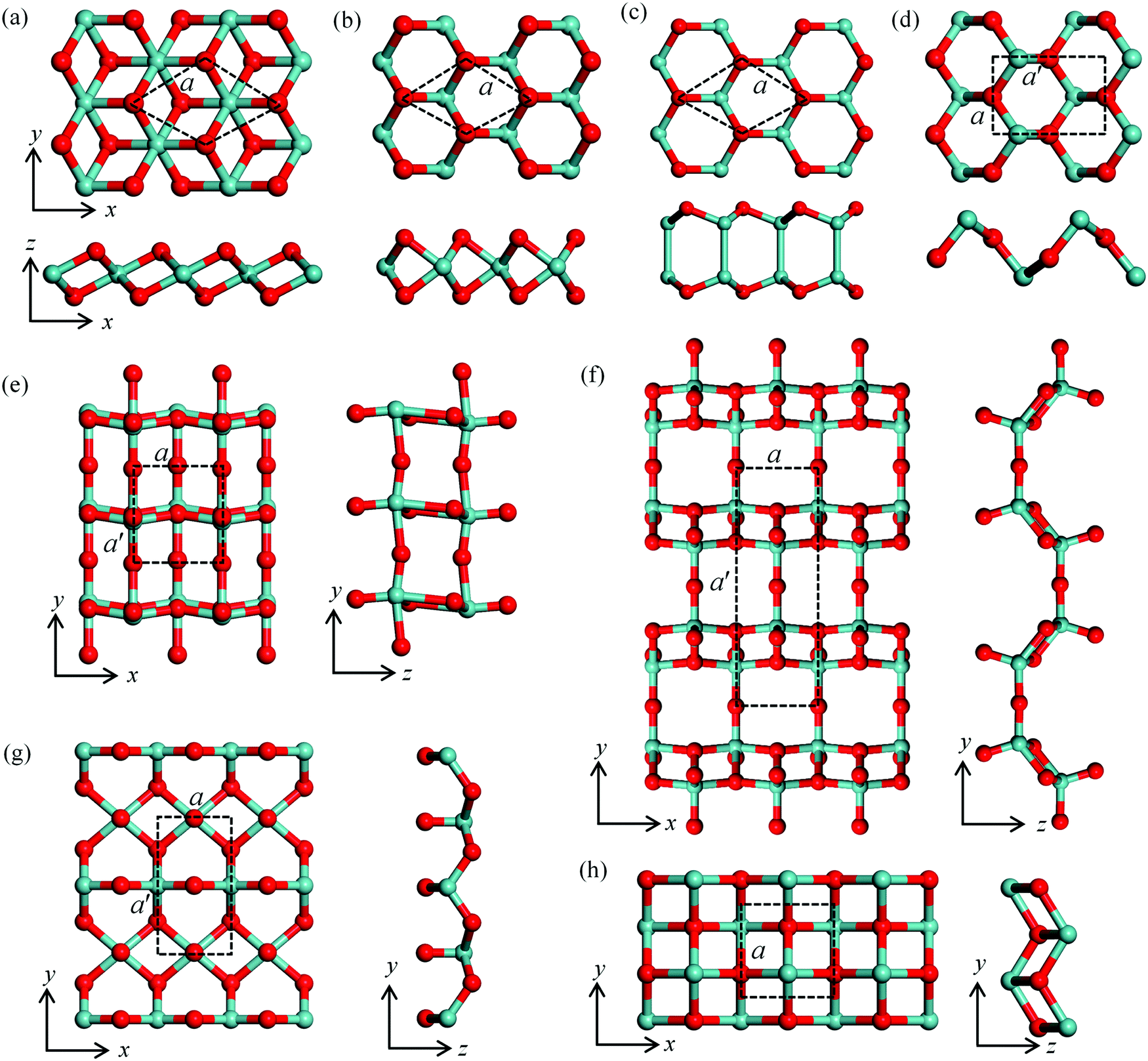 | ||
| Fig. 1 The atomic structures of various monolayer metal oxides: (a) the hexagonal structures in the T phase for ZrOT2, HfOT2, NiOT2, PtOT2, GeOT2 and SnOT2 monolayers (the superscript “T” indicates T phase). (b) The hexagonal structures in the H phase including MoOH2, WOH2 and SnOH2 (the superscript “H” indicates H phase). (c), (e), (g) and (h) The structures of InO, MoO3, TiO2 and squared SnO-1 monolayers. (d) and (f) The monolayers of GeO and SnO, and Mo2O5 and W2O5, respectively. The top and bottom panels in (a), (b), (c) and (d) are top and side views, respectively. The left and right panels in (e), (f), (g) and (h) are top and side views, respectively. The lattice constants a/a′ are highlighted by dashed lines. Metal and oxygen atoms are shown in green and red, respectively. | ||
| Materials | a | ΔH | E B | E g | VBM | CBM | E ad |
|---|---|---|---|---|---|---|---|
| Å | eV per atom | eV | |||||
| ZrOT2 | 3.29 | −3.18 | — | 6.00 (i) | −9.07 | −3.06 | 0.053 |
| HfOT2 | 3.24 | −3.36 | — | 6.48 (i) | −8.91 | −2.43 | −0.014 |
| MoOH2 | 2.83 | −1.87 | — | 1.74 (i) | −7.74 | −6.00 | 0.271 |
| WOH2 | 2.83 | −1.94 | — | 2.16 (i) | −7.25 | −5.09 | 0.003 |
| NiOT2 | 2.83 | −0.67 | −0.001 | 3.09 (i) | −9.68 | −6.59 | 0.031 |
| PtOT2 | 3.16 | −0.47 | −0.002 | 3.47 (i) | −8.21 | −4.74 | −0.071 |
| InO | 3.48 | −1.10 | — | 1.22 (i) | −7.26 | −6.05 | 0.092 |
| GeOT2 | 2.92 | −1.51 | — | 5.17 (i) | −10.07 | −4.90 | 0.202 |
| SnOT2 | 3.22 | −1.55 | −0.004 | 4.11 (i) | −9.44 | −5.32 | 0.028 |
| SnOH2 | 3.10 | −1.06 | — | 1.81 (i) | −9.56 | −7.74 | 0.021 |
| TiO2 | 3.14/5.73 | −4.27 | −0.006 | 3.97 (d) | −8.37 | −4.30 | 0.013 |
| MoO3 | 3.70/3.94 | −1.80 | −0.002 | 2.94 (i) | −9.54 | −6.60 | 0.104 |
| Mo2O5 | 3.83/11.11 | −1.94 | −0.003 | 1.36 (d) | −6.54 | −5.18 | 0.002 |
| WO3 | 3.75/3.81 | −2.06 | — | 2.35 (i) | −9.72 | −7.37 | 0.003 |
| W2O5 | 3.84/11.20 | −3.68 | −0.004 | 1.39 (d) | −6.03 | −4.64 | 0.001 |
| GeO | 3.02/4.54 | −1.16 | — | 3.73 (i) | −6.21 | −2.47 | −0.083 |
| SnO | 3.36/5.01 | −1.26 | −0.075 | 3.48 (i) | −5.47 | −2.00 | −0.002 |
| SnO-1 | 3.84 | −1.30 | −0.037 | 3.92 (i) | −5.83 | −1.90 | −0.091 |
To examine the chemical stability of MMOs in the open-air environment, we consider adsorption of an O2 molecule on these 2D sheets. The interaction between O2 and the MMO layer is described by the adsorption energy (Ead) defined as:
| Ead = Eox − Emono − EO2 | (2) |
Knowledge of adsorption and dissociation of water on the surface of 2D materials is of crucial importance for evaluating the use of these metal oxides in humid air environment. To this end, we investigate H2O adsorption and dissociation on MMOs [structure (d–h) in Fig. 1]. Here, we define the adsorption energy (Ead*) to describe the interaction between H2O and the MMO, as follows:
| Ead* = Eox − Emono − EH2O | (3) |
Even the monolayers Mo2O5, W2O5 and TiO2 yield H2O adsorption energies as low as −0.96 eV; H2O is not favored to dissociate into a H atom and a OH radical on the monolayers Mo2O5, W2O5 and TiO2 due to the positive adsorption energy in the range of 1.04–3.05 eV and negative reaction of heat (defined as the energy difference between initial and final states) in the range of −4.01 to −1.63 eV, as shown in Fig. S9 and Table S2 (ESI†). Only TiO2 can easily dissociate H2O into two separated H atoms and one oxygen atom with an exothermic heat of reaction of −0.56 eV. ESI† Fig. S10 illustrates the path for H2O dissociation on the monolayer TiO2. Although the reaction is exothermic, the H2O molecule undergoes a transition to three atoms by overcoming a high activation barrier of 1.84 eV, suggesting a slow rate of H2O dissociation, and modest chemical stability of the monolayer TiO2 in ambient air.
Since the 2D monolayer or few-layer materials are usually fabricated by mechanical exfoliation from their bulk solids, we calculate the interlayer binding energy to assess the ability for exfoliation from bulk counterparts. We define the interlayer binding energy EB as follows:
| EB = (Ebulk − n1 × EML)/n2 | (4) |
Electronic structures and carrier transport properties of monolayer metal oxides
Previously, the geometric and electronic structures of monolayer GeO, SnO, SnO2, MoO2, WO2, MoO3 and NiO2 were studied,25–30 but the carrier mobilities of only MoO3 and SnO monolayers were reported.27,29 Here, the carrier transport properties of the MMOs are systematically investigated. The electronic band structures of the MMOs are presented in Fig. 2, and their bandgaps are given in Table 1. All 18 MMOs are either semiconductors or insulators, with bandgaps ranging from 1.22 to 6.48 eV, which are comparable to the values of other wide band-gap semiconducting 2D materials, like boron monochalcogenides (with bandgap in the range of 2.06–4.00 eV).42 In particular, TiO2, Mo2O5 and W2O5 monolayers possess a direct bandgap. At the HSE06 level of theory, the majority of MMOs considered here, including WOH2, NiOT2, PtOT2, GeOT2, SnOT2, TiO2, MoO3, WO3, GeO, SnO and SnO-1 monolayers, are wide bandgap semiconductors with 5.17 eV > Eg > 2 eV. Thus, these MMOs are suitable for potential applications as electronic and optoelectronic devices to operate at much higher voltages, frequencies and temperatures than the conventional semiconductor materials like silicon and gallium arsenide.43–46 On the other hand, ZrO2 and HfO2 monolayers possess exceptionally large bandgaps of 6.0 and 6.48 eV, and should be considered as 2D insulators. Their carrier transport properties will not be discussed below. Nevertheless, the large bandgaps for monolayer ZrO2 and HfO2 render their possible application in ultraviolet photodetectors.47–49 | ||
| Fig. 2 Electronic band structures of monolayer metal oxides based on the HSE06 functional. Eg is the band gap denoted by the solid blue arrow. High-symmetry points in the first Brillouin zone are Γ (0, 0, 0), K (−0.333, 0.666, 0) and M (0, 0.5, 0) for hexagonal structures, and Γ (0, 0, 0), Y (0, 0.5, 0), Q (0.5, 0.5, 0) and X (0.5, 0, 0) for orthorhombic structures, respectively. | ||
Based on the band structures shown in Fig. 2, the effective masses of carriers for 16 MMOs are calculated and summarized in Table 2. The effective masses are in the range of 0.73–6.73 m0 (0.73–4.52 m0) for holes, and 0.31–6.12 m0 (0.10–6.74 m0) for electrons along the x direction (y direction), respectively. Moreover, MoOH2, WOH2, PtOT2, W2O5 and SnO monolayers (SnOT2, SnOH2, TiO2, MoO3, WO3 and GeO monolayers) exhibit strong directional anisotropy with a longitudinal/horizontal ratio up to 18.4 for electrons (5.1 for holes). The carrier effective mass in this work is distinct from that in ref. 35 since the unit cell or supercell adopted is different, hence the x-direction of the effective mass. The monolayer metal oxides as a photocatalyst for water splitting are demonstrated in ESI,† S7. By comparing the band edges with the redox potentials of water, we identified that monolayer TiO2, GeO, SnO, SnO-1, ZrOT2 and HfOT2 can be potential functional photocatalysts for water splitting at acidic or neutral environments. However, considering the overpotentials for oxygen and hydrogen evolution processes,50 only the GeO monolayer satisfies the basic requirement for water splitting.
| Materials | m h x | m h y | E 1x | E 1y | C x | C y | μ h x | μ h y |
|---|---|---|---|---|---|---|---|---|
| m 0 | eV | J m−2 | cm2 V−1 s−1 | |||||
| MoOH2 | 0.75 | 0.75 | 15.20 | 15.19 | 253.73 | 238.05 | 41.17 | 38.71 |
| WOH2 | 0.73 | 0.73 | 4.97 | 5.50 | 284.37 | 289.63 | 455.89 | 379.18 |
| NiOT2 | 1.96 | 2.01 | 1.39 | 1.53 | 141.77 | 144.29 | 399.26 | 326.01 |
| PtOT2 | 1.34 | 1.33 | 9.14 | 2.11 | 118.29 | 126.51 | 16.64 | 338.89 |
| InO | 2.81 | 2.68 | 4.91 | 5.14 | 100.44 | 103.51 | 11.40 | 11.21 |
| GeOT2 | 3.92 | 3.80 | 4.37 | 4.85 | 175.40 | 175.85 | 12.80 | 10.75 |
| SnOT2 | 6.73 | 3.07 | 5.85 | 5.68 | 151.70 | 152.76 | 3.05 | 7.14 |
| SnOH2 | 3.35 | 5.81 | 3.17 | 3.53 | 159.49 | 169.41 | 22.60 | 11.18 |
| TiO2 | 4.46 | 0.88 | 3.17 | 2.67 | 104.21 | 85.02 | 24.75 | 145.12 |
| MoO3 | 2.91 | 0.91 | 1.07 | 6.50 | 178.65 | 150.01 | 698.56 | 50.78 |
| Mo2O5 | 2.30 | 2.27 | 0.66 | 1.81 | 91.36 | 10.79 | 853.92 | 13.36 |
| WO3 | 2.91 | 1.52 | 7.46 | 10.16 | 197.75 | 198.13 | 12.25 | 12.63 |
| W2O5 | 3.99 | 3.07 | 3.48 | 3.20 | 117.09 | 17.54 | 14.60 | 3.37 |
| GeO | 2.63 | 1.16 | 0.73 | 1.37 | 44.79 | 46.78 | 385.03 | 256.97 |
| SnO | 1.34 | 1.73 | 0.79 | 1.46 | 60.04 | 15.46 | 990.93 | 58.10 |
| SnO-1 | 3.51 | 3.51 | 2.10 | 2.10 | 40.73 | 40.73 | 15.30 | 15.30 |
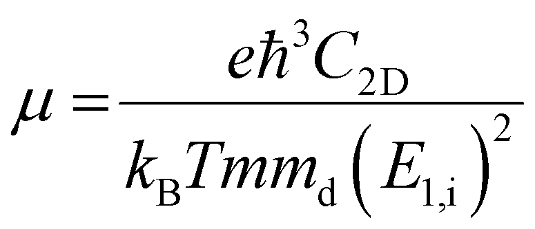
To further estimate the carrier transport properties of MMOs, we calculate their acoustic phonon-limited carrier mobility μ based on the Takagi model within the deformation potential approximation:51,52
 | (5) |
 is the average effective mass (m⊥ is the effective mass perpendicular to the transport direction); C2D is the elastic modulus of the 2D sheet, determined by varying the lattice parameter l along the transport direction via ΔE/S0 = C2D(Δl/l)2/2 (ΔE is the energy change of the system under lattice deformation Δl, S0 is the area of the 2D sheet); the term E1,i represents the deformation potential constant of the valence band maximum (VBM) for a hole or the conduction band minimum (CBM) for an electron along the transport direction, defined by ΔV/(Δl/l) (ΔV is the band edge shift under lattice deformation). All data are calculated using a strain step of 0.5%. The temperature considered in the mobility calculations is 300 K. The present carrier mobility calculation has been evidenced to be not only computationally efficient but also physically reasonable.53,54
The mobilities of electrons and holes calculated by the HSE06 functional are given in Table 3 and schematically shown in Fig. 3. At first glance, the mobilities of electrons ranging from 4.46 to 8541 cm2 V−1 s−1 are substantially larger than those of holes (3.37–990.93 cm2 V−1 s−1). Also note that the carrier mobility shows rather pronounced anisotropy with large longitudinal/horizontal ratio up to 115 (see Table S3, ESI†). This feature could be utilized to enhance the device performance by controlling the direction of carrier transport. Generally speaking, the carrier mobilities of most MMOs are in the order of magnitude of hundreds of cm2 V−1 s−1, which is comparable with those of common 2D materials like phosphorene and MoS2.53,55 More importantly, five monolayers of InO, SnOT2, TiO2, MoO3, SnO and GeO exhibit outstanding electron mobilities above 1000 cm2 V−1 s−1 and even reach up to 8540 cm2 V−1 s−1 for InO, implying that MMOs should be promising candidates for high-speed electronic devices. Our present results, taking MoO3 monolayer as a representative (1466 and 61.86 cm2 V−1 s−1 for electrons, and 698.56 and 50.78 cm2 V−1 s−1 for holes along x and y directions, respectively), are in good agreement with previous theoretical values (1608.80 and 37.52 cm2 V−1 s−1 for electrons, and 800.57 and 25.56 cm2 V−1 s−1 for holes along x and y directions, respectively).29 The 2D elastic contant (C2D) is attained by a quadratic fitting of the total energy versus strain (Fig. S11, ESI†) and the deformation potential constant (E1,i) is calculated by the linear fitting of the CBM (VBM)–strain relation (Fig. S12, ESI†). Furthermore, electronic properties of MMOs containing heavy elements (Hf, Pt, W) are calculated by considering spin–orbit coupling, as displayed in Fig. S13 and Table S4 (ESI†). The results show that electonic properties, including the bandgap, carrier effective mass, deformation potential and carrier mobility, are little influenced by the spin–orbit coupling. For example, after inclusion of the spin–orbit coupling effect, the bandgaps and carrier mobilities change only slightly by 0.03–0.05 eV and 2–40 cm2 V−1 s−1, respectively. Similarly, the electronic properties of MMOs are calculated by using the DFT+U method with Hubbard U parameters of 2.0 eV for Hf, 4.8 eV for Mo, 6.2 eV for W, 5.1 eV for Ni, 3.0 eV for Pt, and 4.2 eV for Ti.38,55–58 The results indicate that the Coulomb interaction results in changes of 0.06–0.25 eV for the band gaps, compared with the values of HSE06 calculation. Meanwhile, carrier mobilities calculated by using the DFT+U method range from 6.89 to 1784.39 cm2 V−1 s−1, a similar trend as calculated by using the HSE06 functional (see Fig. S14 and Table S5, ESI†).
| Materials | m e x | m e y | E 1x | E 1y | C x | C y | μ e x | μ e y |
|---|---|---|---|---|---|---|---|---|
| m 0 | eV | J m−2 | cm2 V−1 s−1 | |||||
| MoOH2 | 6.12 | 0.46 | 10.22 | 3.37 | 253.73 | 238.05 | 5.01 | 579.88 |
| WOH2 | 7.00 | 0.38 | 7.18 | 7.94 | 284.37 | 289.63 | 10.13 | 153.68 |
| NiOT2 | 0.78 | 0.98 | 2.72 | 3.41 | 141.77 | 144.29 | 597.75 | 306.19 |
| PtOT2 | 1.05 | 6.74 | 7.06 | 2.92 | 118.29 | 126.51 | 17.85 | 17.36 |
| InO | 0.33 | 0.10 | 2.47 | 3.76 | 100.44 | 103.51 | 5915.33 | 8540.85 |
| GeOT2 | 0.36 | 0.36 | 8.59 | 8.69 | 175.40 | 175.84 | 386.01 | 378.14 |
| SnOT2 | 0.37 | 0.37 | 2.68 | 2.91 | 151.70 | 152.76 | 3262.75 | 2797.24 |
| SnOH2 | 0.31 | 0.31 | 3.10 | 2.96 | 159.49 | 169.41 | 3563.53 | 4150.41 |
| TiO2 | 2.43 | 3.11 | 7.21 | 2.44 | 104.21 | 85.02 | 6.31 | 24.75 |
| MoO3 | 0.80 | 0.56 | 2.15 | 11.62 | 178.65 | 150.01 | 1466.35 | 61.86 |
| Mo2O5 | 4.28 | 3.66 | 0.50 | 1.72 | 91.36 | 10.79 | 454.00 | 5.32 |
| WO3 | 0.80 | 0.57 | 5.31 | 8.94 | 197.75 | 198.13 | 264.03 | 133.57 |
| W2O5 | 2.08 | 3.96 | 1.54 | 2.65 | 117.09 | 17.54 | 175.24 | 4.64 |
| GeO | 0.41 | 1.74 | 4.34 | 0.50 | 44.79 | 46.78 | 144.29 | 2684.25 |
| SnO | 0.38 | 1.41 | 3.90 | 0.36 | 60.04 | 15.46 | 294.55 | 2473.65 |
| SnO-1 | 0.42 | 0.42 | 3.26 | 3.26 | 40.73 | 40.73 | 444.10 | 444.10 |
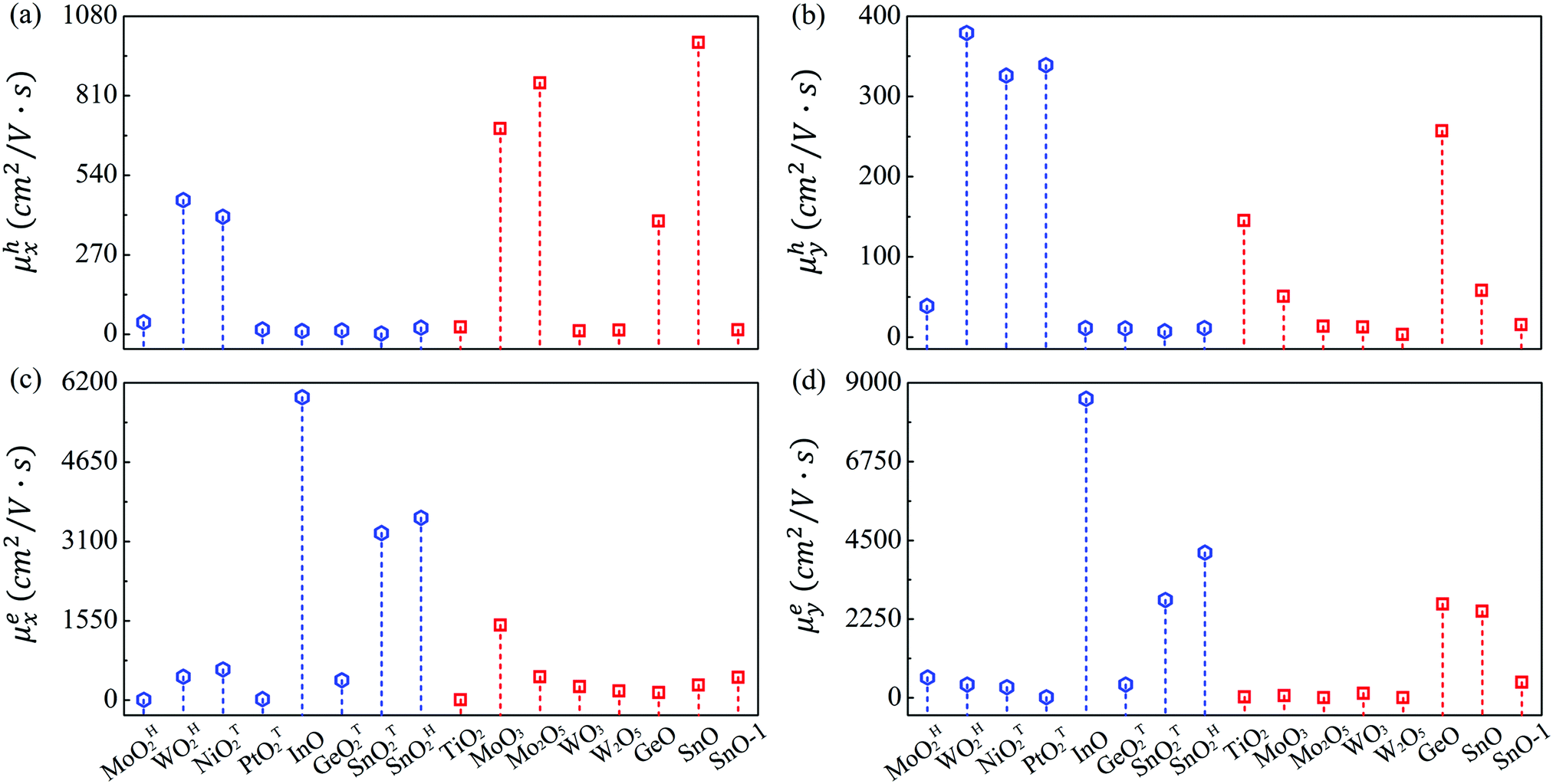 | ||
| Fig. 3 Computed carrier mobility of (a) and (b) holes, and (c) and (d) electrons along the x and y directions. The blue hexagonal and red squares indicate 2D hexagonal and orthorhombic lattice structures, respectively. | ||
Since the experimentally synthesized metal oxide sheets could be multilayer rather than monolayer, we calculate the carrier mobilities of InO bilayer and trilayer. As given in Table S6 (ESI†), multilayer InO sheets still retain ultrahigh carrier mobility up to 7490 cm2 V−1 s−1, rather close to 8540 cm2 V−1 s−1 for InO monolayer. Our results indicate that layered metal oxides hold great promise for the next-generation 2D electronic devices. The high carrier mobility of the 2D metal oxides can be attributed to their relatively small effective mass, large elastic modulus, and small deformation potential constant. These systems show large C2D values up to 290 J m−2, approaching the value of graphene (330 J m−2). In these stiff sheets, the acoustic phonons possess a large group velocity, leading to the small amplitude of lattice waves and weak scattering with charge carriers. The deformation potential constant E1,i is another important factor for carrier mobility. It approximates the strength of electron–phonon coupling and is determined by the band edge shift under lattice variation due to acoustic phonons. E1,i for MMOs could be as low as 0.36 eV, comparable with 0.15 eV of phosphorene,53 which is able to significantly promote the carrier mobility.
Optical absorption properties of monolayer metal oxides
Semiconductors with wide bandgaps can serve as potential visible-blind ultraviolet photodetectors. To this end, we computed optical absorption coefficients of several MMOs with wide bandgap in the ultraviolet region (i.e., wavelength from 10 nm to 400 nm), as shown in Fig. 4 and Fig. S15 (ESI†). Mostly, the optical absorption coefficients can reach as high as 105 cm−1, comparable to that of zincblende, rock salt and wurtzite AlN.43,59 The majority of MMOs exhibit outstanding optical adsorption properties at far ultraviolet (wavelength range of 122–200 nm). In particular, the optical absorption coefficient of ZrOT2 monolayer exhibits a value of nearly 106 cm−1 at a wavelength of ∼69 nm. Prototype devices of ultraviolet detectors made up of h-BN and group-IV chalcogenide sheets have been demonstrated in previous experiments.60–62 The h-BN based deep ultraviolet optical sensor showed very good response to ultraviolet light with wavelengths below 254 nm.63 The detector by group-IV chalcogenide films (such as SnS2) exhibited a remarkable photoresponse above 300 nm, dependence of photocurrent on optical power and wavelength, fast-response, and excellent photo-switch and long-term stability.64,65 By analogy, the present monolayer MMOs with wide bandgap could be promising functional materials for ultraviolet detectors.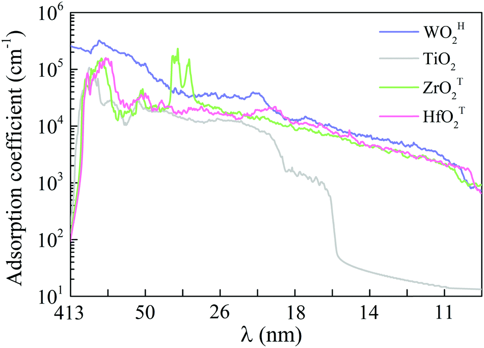 | ||
| Fig. 4 Optical absorption coefficients in the ultraviolet wavelength region for monolayer WOH2, TiO2, ZrOT2 and HfOT2. λ is the wavelength. | ||
Conclusion
We have theoretically explored the atomic structures, energetic stability, electronic and optical properties of 18 monolayer metal oxides. Among them, the most stable structures of 9 monolayer metal oxides are predicted from the unbiased particle-swarm optimization while structures of the other 9 monolayer metal oxides can be simply exfoliated from the bulk counterparts. All 18 monolayer metal oxides are energetically favorable with negative formation energies of −4.27 to −0.47 eV per atom, suggesting high experimental feasibility for the synthesis or mechanical exfoliation of the monolayers. Many of these monolayer metal oxides are wide bandgap semiconductors with chemical inertness, and some entail high carrier mobility up to 8540 cm2 V−1 s−1 as well as pronounced in-plane anisotropy of the carrier mobility with large longitudinal/horizontal ratio up to 115. Moreover, the computed band gaps and band edge positions of monolayer TiO2, GeO, SnO, SnO-1, ZrOT2 and HfOT2 suggest their potential applications as functional photocatalysts for water splitting at acidic or neutral environments. Several monolayer metal oxides also exhibit notable absorption spectra in the ultraviolet wavelength region, with adsorption coefficients above 105 cm−1. Hence, these monolayer metal oxides with band gaps in the range of 1.22–6.48 eV may serve as functional 2D materials in visible light or ultraviolet photodetectors, as well as high-temperature and high-power electronic devices for electron and hole transport.Computational methods
Density functional theory (DFT) calculations66 were performed by using the Vienna ab initio simulation package 5.4.67 More specifically, we used the planewave basis set with an energy cutoff of 500 eV,68 the projector augmented wave (PAW) potentials,69 and the generalized gradient approximation parameterized by Perdew, Burke and Ernzerhof (PBE) for the exchange–correlation functional.70 Since the conventional GGA functional like PBE tends to underestimate the band gaps, a hybrid functional (HSE06) was used to compute the electronic structures and optical properties of the 18 metal oxide sheets. The convergence criterion of total energy was set to 10−7 eV. The geometry optimization was considered to be successful when the residual force on each atom was less than 0.01 eV Å−1. Uniform k-point meshes with spacing of ∼0.015 Å−1 were adopted to sample the 2D Brillouin zones. A vacuum region of 15 Å was added to the vertical direction to avoid interactions between the neighboring layers. The Grimme's DFT-D3 scheme71 was adopted to describe the long-range vdW interactions for computing the interlayer cohesive energy and O2 adsorption energy. Phonon dispersion analysis was performed by using the Phonopy code72 interfaced with the density functional perturbation theory (DFPT) as implemented in VASP.73In total, 18 monolayer metal oxides were considered in this work – MxOy (M = Zr, Hf, Mo, W, Ni, Pt, In, Ge and Sn; x = 1, 2; y = 1, 2, 3, 5). Since bulk NiOT2, PtOT2, SnOT2 (the superscript “T” indicates T phase74), TiO2, MoO3, Mo2O5, W2O5, SnO and SnO-1 exhibit layered structures,37,38 their monolayer sheets could be obtained via mechanical exfoliation. For these systems, we can simply take a monolayer from the corresponding bulk crystal as the initial structure. For MoOH2, WOH2, InO, GeOT2, SnOH2, WO3, GeO, ZrOT2 and HfOT2 (the superscript “H” indicates H phase75), we employed the particle-swarm optimization (PSO) method as implemented in CALYPSO code,76,77 to seek the most stable monolayer structures. As a global optimization method, the PSO algorithm has been successfully used to predict many stable structures of 2D materials.78–80 In our PSO search, the population size was set to 30, and the number of generations was maintained at 30. The required structural relaxations were performed by using the PBE functional, implemented in VASP 5.4 code.
Conflicts of interest
There are no conflicts to declare.Acknowledgements
This work was supported by Science Challenge Project (TZ2018004), the National Natural Science Foundation of China (11574040, 21803002), and the Fundamental Research Funds for the Central Universities of China (DUT17LAB19). Y. G. is supported by China Scholarship Council (CSC 201706060138). We acknowledge the computing resources from the Supercomputing Center of Dalian University of Technology and the University of Nebraska Holland Computing Center.References
- Y. Pan, L. Zhang, L. Huang, L. Li, L. Meng, M. Gao, Q. Huan, X. Lin, Y. Wang, S. Du, H.-J. Freund and H.-J. Gao, Small, 2014, 10, 2215–2225 CrossRef CAS PubMed.
- Z. Sun, A. Martinez and F. Wang, Nat. Photonics, 2016, 10, 227 CrossRef CAS.
- K. S. Novoselov, A. K. Geim, S. V. Morozov, D. Jiang, Y. Zhang, S. V. Dubonos, I. V. Grigorieva and A. A. Firsov, Science, 2004, 306, 666 CrossRef CAS PubMed.
- L. Li, Y. Yu, G. J. Ye, Q. Ge, X. Ou, H. Wu, D. Feng, X. H. Chen and Y. Zhang, Nat. Nanotechnol., 2014, 9, 372 CrossRef CAS PubMed.
- K. Novoselov, Nat. Mater., 2007, 6, 720 CrossRef CAS PubMed.
- Y. Guo, S. Zhou, Y. Bai and J. Zhao, ACS Appl. Mater. Interfaces, 2017, 9, 12013–12020 CrossRef CAS PubMed.
- X. Yu, T. J. Marks and A. Facchetti, Nat. Mater., 2016, 15, 383 CrossRef CAS PubMed.
- I. Ferain, C. A. Colinge and J.-P. Colinge, Nature, 2011, 479, 310 CrossRef CAS PubMed.
- M.-G. Kim, M. G. Kanatzidis, A. Facchetti and T. J. Marks, Nat. Mater., 2011, 10, 382 CrossRef CAS PubMed.
- A. Zavabeti, J. Z. Ou, B. J. Carey, N. Syed, R. Orrell-Trigg, E. L. H. Mayes, C. Xu, O. Kavehei, A. P. O’Mullane, R. B. Kaner, K. Kalantar-zadeh and T. Daeneke, Science, 2017, 358, 332 CrossRef CAS PubMed.
- J. You, C.-C. Chen, L. Dou, S. Murase, H.-S. Duan, S. A. Hawks, T. Xu, H. J. Son, L. Yu, G. Li and Y. Yang, Adv. Mater., 2012, 24, 5267–5272 CrossRef CAS PubMed.
- K. An, Q. Zhang, S. Alayoglu, N. Musselwhite, J.-Y. Shin and G. A. Somorjai, Nano Lett., 2014, 14, 4907–4912 CrossRef CAS PubMed.
- W. He, W. Xu, Q. Peng, C. Liu, G. Zhou, S. Wu, M. Zeng, Z. Zhang, J. Gao, X. Gao, X. Lu and J. M. Liu, J. Phys. Chem. C, 2016, 120, 9949–9957 CrossRef CAS.
- M. Gutowski, J. E. Jaffe, C.-L. Liu, M. Stoker, R. I. Hegde, R. S. Rai and P. J. Tobin, Appl. Phys. Lett., 2002, 80, 1897–1899 CrossRef CAS.
- L. Wang and T. Sasaki, Chem. Rev., 2014, 114, 9455–9486 CrossRef CAS PubMed.
- S. Balendhran, J. Deng, J. Z. Ou, S. Walia, J. Scott, J. Tang, K. L. Wang, M. R. Field, S. Russo, S. Zhuiykov, M. S. Strano, N. Medhekar, S. Sriram, M. Bhaskaran and K. Kalantar-zadeh, Adv. Mater., 2013, 25, 109–114 CrossRef CAS PubMed.
- N. D. Arora, J. R. Hauser and D. J. Roulston, IEEE Trans. Electron Devices, 1982, 29, 292–295 Search PubMed.
- Y. C. Song, Y. H. Kang, J. Y. Jung, S. Y. Nam, J. Lim, S. C. Yoon, H. C. Dong and C. Lee, Chem. Mater., 2012, 24, 3517–3524 CrossRef.
- H. Huang, H. Gong, C. L. Chow, J. Guo, T. J. White, M. S. Tse and O. K. Tan, Adv. Funct. Mater., 2011, 21, 2680–2686 CrossRef CAS.
- M. Tadatsugu, N. Yuki and M. Toshihiro, Appl. Phys. Express, 2013, 6, 044101 CrossRef.
- Y. Choi, G. H. Kim, W. H. Jeong, H. J. Kim, B. D. Chin and J.-W. Yu, Thin Solid Films, 2010, 518, 6249–6252 CrossRef CAS.
- D. Spiehl, M. Häming, H. M. Sauer, K. Bonrad and E. Dörsam, IEEE Trans. Electron Devices, 2015, 62, 2871–2877 CAS.
- J. Leppäniemi, O.-H. Huttunen, H. Majumdar and A. Alastalo, Adv. Mater., 2015, 27, 7168–7175 CrossRef PubMed.
- U. Betz, M. Kharrazi Olsson, J. Marthy, M. F. Escolá and F. Atamny, Surf. Coat. Technol., 2006, 200, 5751–5759 CrossRef CAS.
- J. A. Reyes-Retana and F. Cervantes-Sodi, Sci. Rep., 2016, 6, 24093 CrossRef CAS PubMed.
- C. Kamal, A. Chakrabarti and M. Ezawa, Phys. Rev. B, 2016, 93, 125428 CrossRef.
- J. Du, C. Xia, Y. Liu, X. Li, Y. Peng and S. Wei, Appl. Surf. Sci., 2017, 401, 114–119 CrossRef CAS.
- W.-Z. Xiao, G. Xiao and L.-L. Wang, J. Chem. Phys., 2016, 145, 174702 CrossRef PubMed.
- W. B. Zhang, Q. Qu and K. Lai, ACS Appl. Mater. Interfaces, 2017, 9, 1702–1709 CrossRef CAS PubMed.
- F. Haque, T. Daeneke, K. Kalantar-zadeh and J. Z. Ou, Nano-Micro Lett., 2017, 10, 23 CrossRef PubMed.
- J. Tao and L. Guan, Sci. Rep., 2017, 7, 44568 CrossRef CAS PubMed.
- F. Li and Z. Chen, Nanoscale, 2013, 5, 5321–5333 RSC.
- C. C. Leong, H. Pan and S. K. Ho, Phys. Chem. Chem. Phys., 2016, 18, 7527–7534 RSC.
- L. Seixas, A. S. Rodin, A. Carvalho and A. H. C. Neto, Phys. Rev. Lett., 2016, 116, 206803 CrossRef CAS PubMed.
- H. Sten, S. Mikkel, P. Mohnish, D. Thorsten, S. S. Per, F. H. Nicki, N. G. Morten, T. Daniele, M. L. Peter, C. R.-J. Anders, G. Jakob, W. J. Karsten, M. Jens Jørgen, O. Thomas and S. T. Kristian, 2D Mater., 2018, 5, 042002 CrossRef.
- A. Ziletti, A. Carvalho, D. K. Campbell, D. F. Coker and A.H. Castro Neto, Phys. Rev. Lett., 2015, 114, 046801 CrossRef CAS PubMed.
- L. C. P. Villars, American Society of Metals, Cleveland, OH, 1985 Search PubMed.
- K. Persson, https://materialsproject.org/.
- H. Peelaers and C G. V. d. Walle, J. Phys.: Condens. Matter, 2014, 26, 305502 CrossRef CAS PubMed.
- Y. Cai, G. Zhang and Y.-W. Zhang, Sci. Rep., 2014, 4, 6677 CrossRef CAS PubMed.
- G. Gabriella, K. Jiří, F.-A. Felix and M. Angelos, J. Phys.: Condens. Matter, 2012, 24, 424216 CrossRef PubMed.
- B. Mortazavi and T. Rabczuk, Energies, 2018, 11, 1573 CrossRef.
- E. Monroy, F. Omnès and F. Calle, Semicond. Sci. Technol., 2003, 18, R33 CrossRef CAS.
- J. L. Hudgins, G. S. Simin, E. Santi and M. A. Khan, IEEE Trans. Power Electron., 2003, 18, 907–914 CrossRef.
- P. G. Neudeck, R. S. Okojie and C. Liang-Yu, Proc. IEEE, 2002, 90, 1065–1076 CrossRef.
- T. P. Chow and R. Tyagi, IEEE Trans. Electron Devices, 1994, 41, 1481–1483 CrossRef CAS.
- J. Xing, E. Guo and H. Lu, Sci. China: Phys., Mech. Astron., 2011, 54, 1416–1419 CAS.
- J. Seol, G. Lee and S. Hahm, IEEE Sens. J., 2018, 18, 4477–4481 Search PubMed.
- C. Chin-Hsiang, T. Yu-Hsuan, T. Sung-Yi and C. Chung-Fu, Jpn. J. Appl. Phys., 2011, 50, 04DG19 CrossRef.
- I. E. Castelli, D. D. Landis, K. S. Thygesen, S. Dahl, I. Chorkendorff, T. F. Jaramillo and K. W. Jacobsen, Energy Environ. Sci., 2012, 5, 9034–9043 RSC.
- S. Bruzzone and G. Fiori, Appl. Phys. Lett., 2011, 99, 222108 CrossRef.
- S. Takagi, A. Toriumi, M. Iwase and H. Tango, IEEE Trans. Electron Devices, 1994, 41, 2357–2362 CrossRef CAS.
- J. Qiao, X. Kong, Z.-X. Hu, F. Yang and W. Ji, Nat. Commun., 2014, 5, 4475 CrossRef CAS PubMed.
- Y. Guo, S. Zhou, J. Zhang, Y. Bai and J. Zhao, 2D Mater., 2016, 3, 025008 CrossRef.
- K. Kaasbjerg, K. S. Thygesen and A.-P. Jauho, Phys. Rev. B: Condens. Matter Mater. Phys., 2013, 87, 235312 CrossRef.
- Z. Xie, S. Lin and Z. Wang, Ceram. Int., 2018, 44, 15912–15917 CrossRef CAS.
- Y.-F. Zhang, H. Ren and Z.-T. Hou, J. Magn. Magn. Mater., 2015, 375, 61–64 CrossRef CAS.
- D. Wang, Z.-P. Liu and W.-M. Yang, ACS Catal., 2018, 8, 7270–7278 CrossRef CAS.
- Z.-Y. Jiao, S.-H. Ma and J.-F. Yang, Solid State Sci., 2011, 13, 331–336 CrossRef CAS.
- F. Xia, H. Wang, D. Xiao, M. Dubey and A. Ramasubramaniam, Nat. Photonics, 2014, 8, 899 CrossRef CAS.
- K. Watanabe, T. Taniguchi and H. Kanda, Nat. Mater., 2004, 3, 404 CrossRef CAS PubMed.
- J. Wang, H. Fang, X. Wang, X. Chen, W. Lu and W. Hu, Small, 2017, 13, 1700894 CrossRef PubMed.
- M. Sajjad, W. M. Jadwisienczak and P. Feng, Nanoscale, 2014, 6, 4577–4582 RSC.
- Y. Tao, X. Wu, W. Wang and J. Wang, J. Mater. Chem. C, 2015, 3, 1347–1353 RSC.
- J.-J. Wu, Y.-R. Tao, Y. Wu and X.-C. Wu, Sens. Actuators, B, 2016, 231, 211–217 CrossRef CAS.
- W. Kohn and L. J. Sham, Phys. Rev., 1965, 140, A1133–A1138 CrossRef.
- G. Kresse and J. Furthmüller, Phys. Rev. B: Condens. Matter Mater. Phys., 1996, 54, 11169–11186 CrossRef CAS.
- P. E. Blöchl, Phys. Rev. B: Condens. Matter Mater. Phys., 1994, 50, 17953–17979 CrossRef.
- G. Kresse and D. Joubert, Phys. Rev. B: Condens. Matter Mater. Phys., 1999, 59, 1758–1775 CrossRef CAS.
- J. P. Perdew, K. Burke and M. Ernzerhof, Phys. Rev. Lett., 1996, 77, 3865–3868 CrossRef CAS PubMed.
- S. Grimme, J. Antony, S. Ehrlich and H. Krieg, J. Chem. Phys., 2010, 132, 154104 CrossRef PubMed.
- A. Togo, F. Oba and I. Tanaka, Phys. Rev. B: Condens. Matter Mater. Phys., 2008, 78, 134106 CrossRef.
- S. Baroni, S. de Gironcoli, A. Dal Corso and P. Giannozzi, Rev. Mod. Phys., 2001, 73, 515–562 CrossRef CAS.
- M. Acerce, D. Voiry and M. Chhowalla, Nat. Nanotechnol., 2015, 10, 313 CrossRef CAS PubMed.
- X. Fan, P. Xu, D. Zhou, Y. Sun, Y. C. Li, M. A. T. Nguyen, M. Terrones and T. E. Mallouk, Nano Lett., 2015, 15, 5956–5960 CrossRef CAS PubMed.
- Y. Wang, M. Miao, J. Lv, L. Zhu, K. Yin, H. Liu and Y. Ma, J. Chem. Phys., 2012, 137, 224108 CrossRef PubMed.
- Y. Wang, J. Lv, L. Zhu and Y. Ma, Phys. Rev. B: Condens. Matter Mater. Phys., 2010, 82, 094116 CrossRef.
- Y. Guo, Q. Wu, Y. Li, N. Lu, K. Mao, Y. Bai, J. Zhao, J. Wang and X. C. Zeng, Nanoscale Horiz., 2019 10.1039/c8nh00216a.
- X. Luo, J. Yang, H. Liu, X. Wu, Y. Wang, Y. Ma, S. H. Wei, X. Gong and H. Xiang, J. Am. Chem. Soc., 2011, 133, 16285–16290 CrossRef CAS PubMed.
- V. S. Bhadram, H. Liu, E. Xu, T. Li, V. B. Prakapenka, R. Hrubiak, S. Lany and T. A. Strobel, Phys. Rev. Mater., 2018, 2, 011602 CrossRef.
Footnote |
| † Electronic supplementary information (ESI) available. See DOI: 10.1039/c8nh00273h |
| This journal is © The Royal Society of Chemistry 2019 |