
Efficient hole transfer from monolayer WS2 to ultrathin amorphous black phosphorus†
Matthew Z.
Bellus
a,
Zhibin
Yang
b,
Peymon
Zereshki
a,
Jianhua
Hao
 b,
Shu Ping
Lau
b and
Hui
Zhao
*a
b,
Shu Ping
Lau
b and
Hui
Zhao
*a
aDepartment of Physics and Astronomy, The University of Kansas, Lawrence, Kansas 66045, USA. E-mail: huizhao@ku.edu
bDepartment of Applied Physics, The Hong Kong Polytechnic University, Hung Hom Kowloon, Hong Kong, People's Republic of China
First published on 2nd October 2018
Abstract
The newly developed van der Waals materials allow fabrication of multilayer heterostructures. Early efforts have mostly focused on heterostructures formed by similar materials. More recently, however, attempts have been made to expand the types of materials, such as topological insulators and organic semiconductors. Here we introduce an amorphous semiconductor to the material library for constructing van der Waals heterostructures. Samples composed of 2 nm amorphous black phosphorus synthesized by pulsed laser deposition and monolayer WS2 obtained by mechanical exfoliation were fabricated by dry transfer. Photoluminescence measurements revealed that photocarriers excited in WS2 of the heterostructure transfer to amorphous black phosphorus, in the form of either energy or charge transfer, on a time scale shorter than the exciton lifetime in WS2. Transient absorption measurements further indicate that holes can efficiently transfer from WS2 to amorphous black phosphorus. However, interlayer electron transfer in either direction was found to be absent. The lack of electron transfer from amorphous black phosphorus to WS2 is attributed to the localized electronic states in the amorphous semiconductor. Furthermore, we show that a hexagonal BN bilayer can effectively change the hole transfer process.
Conceptual insightsWe introduce an amorphous semiconductor to the material library for constructing van der Waals heterostructures. Since 2014, van der Waals heterostructures have been one of the most dynamic research topics in nanoscience and nanotechnology. Previous efforts have mostly been focused on combining two materials with similar lattices, such as different types of transition metal dichalcogenides. However, heterostructures combining materials with different lattice structures can potentially allow integration of vastly different properties. Here we explore an extreme example by combining a crystalline monolayer with an amorphous ultrathin film. We fabricate heterostructures composed of a 2 nm amorphous black phosphorus layer and a monolayer of WS2. Time-integrated photoluminescence and time-resolved transient absorption measurements both revealed that holes excited in WS2 can efficiently transfer to amorphous black phosphorus on an ultrafast time scale. Furthermore, we show that a hexagonal BN bilayer can effectively control the hole transfer process. These results establish amorphous black phosphorus as a building block for van der Waals heterostructures, provide new information for understanding interlayer charge transfer, and allow electrical connections to amorphous materials by van der Waals interfaces. |
1 Introduction
Recently, two-dimensional (2D) materials have drawn considerable attention for both fundamental research and applications due to their novel electronic and optical properties.1–5 One of the intriguing aspects of these materials is that they can form multilayer heterostructures via van der Waals interlayer interaction.6 Unlike ionic and covalent bonds, van der Waals interaction does not have atomic-level correspondence. This is a significant advantage over traditional heterostructures that can only be formed by materials with similar lattice structures. Since lattice mismatch is no longer a constraint, a large number of materials can be chosen from to assemble multilayers with certain properties. Hence, this new approach can produce a vast number of new materials for many applications, and can potentially transform material discovery.7,8 The interfaces in such structures are atomically sharp and the junctions can be as thin as two atomic layers – both reaching the ultimate limit.Since 2013, the study of van der Waals heterostructures has gained significant momentum. The majority of the efforts have been devoted to heterobilayers formed by transition metal dichalcogenides (TMDs) and graphene or by two types of TMDs. Combining graphene with TMD is beneficial for optoelectronic applications,9–12 since the former can serve as electrodes13 while the latter, the light absorption or emission layer.14 Study of TMD–TMD heterobilayers can provide valuable information on van der Waals interlayer coupling, and allow tuning of the optical and transport properties of these materials.15–24 In these van der Waals heterostructures, the two materials have similar lattice structures. Layer-coupled states can form, which can help integrate electronic and optical properties of the two materials. For example, layer-coupled states could be responsible for the observed ultrafast interlayer charge transfer in TMD–TMD heterobilayers.25
The removal of lattice-matching requirements invites inclusion of materials with different lattice properties to form heterostructures. In principle, combining 2D materials with different lattice structures (and thus likely different properties) can produce heterostructures with widely tunable properties. Demonstration of high-performance van der Waals heterostructures of materials with significantly different lattice structures will expand the material library and vastly increase the possible material combinations. Very recently, a number of 2D materials with different lattice structures have been used to successfully form heterostructures with TMD and graphene, including phosphorene,26–29 GaTe,30 Bi2Se2,31 CrI3,32 and even organic materials.33–37
Here we introduce a noncrystalline semiconductor, namely amorphous black phosphorus (aBP), to the 2D heterostruture library. Amorphous semiconductors are of great importance in the electronics industry. They are an interesting class of materials, as their amorphous structure omits one of the most fundamental characteristics utilized in solid state physics, crystallinity. The lack of long-range periodicity often leads to very fuzzy electronic states and poor electronic performance compared to their crystalline counterparts. However, low fabrication costs make this type of material highly desirable for applications that do not require superior performance. Most notably, amorphous silicon has been widely used for common photovoltaic devices38 and thin-film transistors.39 Amorphous In–Ga–Zn–O has shown promise for transparent thin-film transistors with reported mobilities exceeding 10 cm2 V−1 s−1.40 Additionally, amorphous SiO2 is widely used as a gate dielectric in the electronics industry. Amorphous materials have also been used as reaction catalysts, with amorphous iron being used to aid in the hydrogenation of carbon monoxide,41 and amorphous metal-oxides as an oxygen evolution reaction catalyst.42
In this work, we fabricate heterostructures of monolayer WS2 and 2 nm aBP, and study their charge carrier dynamics. Recently, ultrathin films of aBP have been successfully synthesized by some of us, along with other collaborators.43 We found that in WS2/aBP heterostructures, holes excited in WS2 transfer to aBP on an ultrafast time scale. Electrons, on the other hand, do not transfer, either from WS2 to aBP or in the opposite direction. The charge transfer results in extended lifetime of photoexcited electrons in WS2. We also show that a hexagonal BN (hBN) bilayer can slow down the hole transfer. These results introduce amorphous semiconductors to the library of building blocks for van der Waals heterostructures, provide a new ingredient for understanding the mechanisms of interlayer charge transfer, and offer a method to make electrical connections to amorphous materials through other 2D crystalline materials.
2 Experimental
2.1 Sample fabrication
Amorphous black phosphorus ultrathin films were synthesized on Si/SiO2 by pulsed laser deposition. A BP crystal was used as the target. The growth temperature was set at 150 °C and the base pressure of the chamber was evacuated to 1.5 × 10⁻⁷ Torr. The nominal thickness of the film is 2 nm, according to previously established synthesis conditions.43The heterostructure samples were made by mechanically exfoliating and subsequently transferring monolayer flakes of WS2 onto the aBP-covered substrate. In order to create reasonable control conditions, we first transferred flakes of hBN with varying thicknesses onto regions of the aBP substrates. This is done by mechanically exfoliating flakes of hBN from bulk crystals onto PDMS substrates. The hBN flakes are then transferred onto the aBP-covered substrate. Next, monolayer WS2 flakes were similarly exfoliated onto PDMS substrates and identified by optical contrast. Using the same method as with hBN, they were transferred to the aBP sample, with different regions of the same WS2 flake overlapping both the hBN layers and the aBP substrate. After the WS2 was transferred, the samples were annealed for 2 h at 75 °C in an Ar environment held at a base pressure of 3 Torr. This is to help the van der Waals materials adhere better to the aBP. Next, to help preserve the aBP surface from degrading in the ambient conditions of our measurements, the samples were spin coated by a thin layer of PMMA.
2.2 Photoluminescence spectroscopy
The PL spectroscopy measurements were carried out under 405 nm continuous-wave laser excitation. The laser beam was focused by a microscope objective lens at normal incident. The laser spot is about 1 μm in full width at half maximum, and is located at the central part of a desired sample region. The power of the laser was controlled by a combination of a half-wave plate and a polarizer. The PL from the sample was collected by the same objective lens and directed into a spectrometer, which is equipped with a thermoelectrically cooled charge-coupled-device camera. To prevent unwanted light from reaching the spectrometer and affecting the measurement, a set of filters was placed before the spectrometer.2.3 Transient absorption measurements
In the transient absorption setup, a Ti:sapphire laser generates 100 fs pulses with a central wavelength tunable from 750 to 850 nm and a repetition rate of 80 MHz. Part of this beam was used to pump an optical parametric oscillator, which outputs a signal pulse tunable from 1100 to 1580 nm. The spectral range can be further extended by second harmonic generation of each output by using a beta barium borate crystal. Depending on the configuration, two of these pulses were used as pump and probe pulses.In each configuration, the pump and probe beams were linearly polarized along perpendicular directions. A beamsplitter was used to combine the two beams, which were sent to a microscope objective lens and focused to the sample to spot sizes of 1–2 μm in full-width at half-maximum. The reflected probe was collected and collimated by the same objective lens and directed into a biased silicon photodiode, the output of which was measured by a lock-in amplifier that is synchronized with a mechanical chopper that modulates the pump intensity at about 2 kHz. We measured the differential reflection, which is defined as ΔR/R0 = (R − R0)/R0, where R and R0 are the reflectivities of the probe by the sample with and without the presence of the pump beam, respectively.
3 Results and discussion
3.1 Sample and photoluminescence
Fig. 1(a) shows an optical microscope image of the sample studied. A uniform 2 nm aBP layer was deposited on a Si/SiO2 substrate, as shown as the pinkish colored background. To study effects of potential charge transfer between WS2 and aBP, we first transferred a thick hBN flake on aBP (outlined by the white line). It contains more than 15 layers. We then transferred monolayer (ML) WS2 (outlined by blue) near the edge of the hBN flake. The region directly on aBP forms the heterostructure sample, while that on hBN serves as an isolated WS2 ML for comparison, since the thick hBN layer is expected to block the interactions between WS2 and aBP effectively.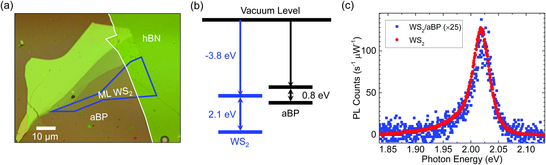 | ||
| Fig. 1 (a) Optical microscope images of the WS2/aBP sample. ML WS2 is outlined by blue and hBN by white. Part of the WS2 is directly on top of aBP, while the rest is on the hBN flake. (b) The expected band alignment of ML WS2 and aBP. (c) Photoluminescence spectra of ML WS2 directly on aBP (blue squares, multiplied by 25) and on hBN (referred to as WS2, red circles). | ||
From first-principle calculations, the electron affinity and the ionization potential of ML WS2 are −3.8 and −5.9 eV, respectively,44 as schematically shown in Fig. 1(b). Based on previous measurements, the optical bandgap of 2 nm aBP is about 0.8 eV.43 However, information on the electron affinity and ionization potential of aBP is still missing. To speculate the nature of the band alignment of the WS2-aBP heterostructure, one could use the values of crystalline BP as a reference. The bandstructure of crystalline BP is highly sensitive to thickness. Hence, one should use the values that best represent the 2 nm thick aBP, which correlates to about 3 layers. The calculated electron affinity of trilayer BP is about −4 eV.45 Using the 2 nm bandgap of aBP of 0.8 eV, an ionization potential of −4.8 eV could be inferred. Given that this value is about 1.1 eV higher than that of WS2, it appears safe to assume that the valence band maximum (VBM) of aBP is above that of WS2. However, since the electron affinities of the two materials are similar, the band alignment of WS2/aBP could be either type-II, as indicated in Fig. 1(b), or type-I with the conduction band minimum (CBM) of aBP below that of WS2. In the following discussions, we will present evidence that the alignment is indeed type-II.
The sample was characterized by using photoluminescence (PL) spectroscopy. A continuous-wave 405 nm laser was focused through a 100× objective lens onto the sample. When the laser spot was placed on the WS2 region on hBN, a strong PL peak at about 2.02 eV was observed (red circles). The PL yield, peak energy, and lineshape are all consistent with previous reports.46–49 This confirms the ML thickness of the WS2 and the effectiveness of the thick hBN layer separating WS2 and aBP. In the rest of these discussions, we will refer to this region of the sample as ML WS2. With the laser spot moved to the region of WS2 that is directly on top of aBP, there is significant quenching of the PL, by about a factor of 25 (blue squares). This quenching indicates that charge or energy transfer occurred from WS2 to aBP. Without such transfer, excitons would be expected to stay in WS2 and recombine, contributing to the PL signal. The large quenching factor suggests that such transfer occurs on a time scale that is much shorter than the exciton lifetime in an individual WS2 ML.
3.2 Ultrafast hole transfer from WS2 to aBP
The PL quenching of WS2 by aBP can originate from charge transfer or energy transfer from WS2 to aBP. In the former case, one type of carrier (likely the holes) transfers to aBP. Although the excited electrons reside in WS2, they are separated from the holes and hence cannot recombine with them and contribute to PL. In energy transfer, both electrons and holes transfer to aBP, which also results in a reduction of WS2 PL yield. To resolve the transfer dynamics and probe the physics mechanisms involved, we performed a transient absorption measurement in reflection geometry.First, we studied photocarrier dynamics in the ML WS2 region. Carriers are injected by a 3.2 eV pump pulse with a peak fluence of 0.46 μJ cm−2. With an absorption coefficient of 0.72 × 10⁶ m−1,14 this corresponds to an injected areal carrier density of 4.37 × 1010 cm−2. The red circles in Fig. 2(a) show the differential reflection signal of a 2.0 eV probe, which is tuned to the A-exciton resonance of ML WS2. The rise of the signal can be fit by the integral of a Gaussian function with a full width at half maximum of 0.37 ps, as indicated by the solid curve in the inset. Since the width of the pump and probe pulses are both about 0.25 ps at the sample location (due to the chirp introduced by the objective lens), this value is close to the instrumental response time. This suggests that the pump-injected electron–hole pairs produce a peak differential reflection signal at the A-exciton resonance on a time scale shorter than the instrumental response time, which is consistent with previous reports.50–52 The decay of the signal can be fit by a bi-exponential function, ΔR/R0(t) = A1![[thin space (1/6-em)]](https://www.rsc.org/images/entities/char_2009.gif) exp(−t/τ1) + A2exp(−t/τ2) + B. The black curve over the symbols shows that the fit is satisfactory, with parameters of A1 = 1.51 × 10⁻³, A2 = 1.19 × 10⁻³, B = 0.08 × 10⁻³, τ1 = 0.59 ± 0.1 ps, and τ2 = 13 ± 1 ps. The bi-exponential dynamics and these time constants are both reasonably consistent with previous reports on ML WS2.50–52 The short time constant of τ1 can be attributed to formation of excitons from the injected electron–hole pairs;50 while the long time constant τ2 indicates the lifetime of excitons.51,52 By increasing the pump fluence, we can confirm that these time constants are independent of the injected carrier density, while the signal magnitude is proportional to the density (see ESI,† Fig. S1). To probe the possible contributions from the aBP layer underneath hBN to the signal, we repeated the measurement with the laser spots located at a region not covered by WS2. The results are shown by the gray triangles in Fig. 2. The lack of a detectable signal is expected,53 since the probe photon energy is much higher than the bandgap of 0.8 eV of the aBP layer.
exp(−t/τ1) + A2exp(−t/τ2) + B. The black curve over the symbols shows that the fit is satisfactory, with parameters of A1 = 1.51 × 10⁻³, A2 = 1.19 × 10⁻³, B = 0.08 × 10⁻³, τ1 = 0.59 ± 0.1 ps, and τ2 = 13 ± 1 ps. The bi-exponential dynamics and these time constants are both reasonably consistent with previous reports on ML WS2.50–52 The short time constant of τ1 can be attributed to formation of excitons from the injected electron–hole pairs;50 while the long time constant τ2 indicates the lifetime of excitons.51,52 By increasing the pump fluence, we can confirm that these time constants are independent of the injected carrier density, while the signal magnitude is proportional to the density (see ESI,† Fig. S1). To probe the possible contributions from the aBP layer underneath hBN to the signal, we repeated the measurement with the laser spots located at a region not covered by WS2. The results are shown by the gray triangles in Fig. 2. The lack of a detectable signal is expected,53 since the probe photon energy is much higher than the bandgap of 0.8 eV of the aBP layer.
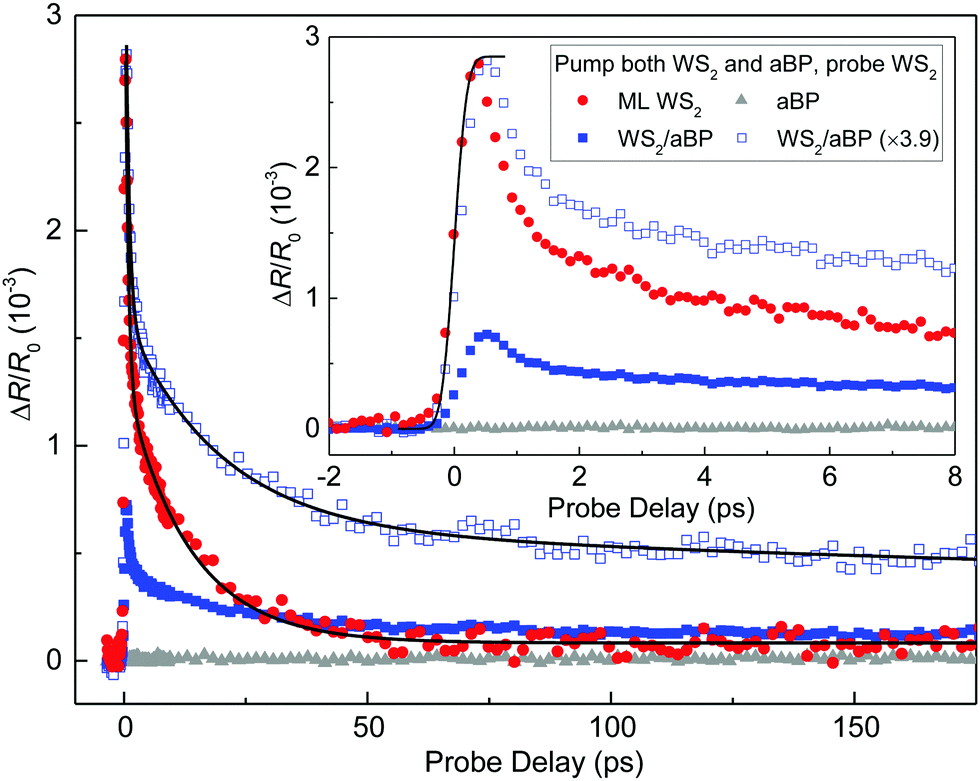 | ||
| Fig. 2 Time-resolved differential reflection measurements with a 3.2 eV pump and a 2.0 eV probe. Solid symbols represent results from different regions of the same sample. Open symbols are scaled for better comparison. The inset provides a closer look at the data near zero probe delay. | ||
We next repeated the measurement by moving the laser spots to the region of WS2/aBP. Without interlayer transfer, one would expect a similar signal since the same density of carriers was injected in WS2 and will produce a signal with the same time evolution, while carriers injected in aBP will not contribute to the signal. However, as shown by the blue solid squares in Fig. 2(a), we observed a signal that is a few times smaller and decays at a slower rate. To better compare this signal with that from the ML WS2 region, it was multiplied by 3.9, as shown by the blue open squares. Clearly, the majority of the signal decays slower than ML WS2. The significant differences in both the magnitude and the dynamics of the two signals strongly suggest that there is substantial interlayer transfer from WS2 to aBP.
Close examination of the signal from the heterostructure revealed that the scaled signal can be fit by a tri-exponential function, ΔR/R0(t) = A1exp(−t/τ1) + A2exp(−t/τ2) + A3exp(−t/τ3) (black curve), with parameters of A1, A2, and A3 of 2.4, 1.0, and 0.6 × 10⁻³, and τ1, τ2, and τ3 of 0.7 ± 0.1, 19.6 ± 2, and 697 ± 150 ps. The sub-ps component contributes to about 60% of the total signal, which is similar to the ML WS2 data. It can be attributed to the same origin of exciton formation. The other two time constants show that the carrier lifetime in WS2 is significantly extended in the heterostructure. Power-dependence measurement also confirms that dynamics is independent of the injected carrier density and the signal magnitude is proportional to the density (see ESI,† Fig. S2).
The possible candidates for interlayer transfer include energy transfer and charge transfer. The energy transfer can be achieved by either a Fröster mechanism,54 where elimination of one exciton in WS2 induces an exciton or electron–hole pair in aBP, or a Dexter mechanism,55,56 where an exciton moves from WS2 to aBP. In both cases, however, the decay of the signal should be faster than ML WS2 since the energy transfer provides an additional channel for reducing the carrier density in WS2. This contradicts the data. On the other hand, charge transfer (either electrons or holes) from WS2 to aBP would leave one type of carrier in WS2, causing a smaller but long-living signal since their recombination will be suppressed by charge separation. Both these features are consistent with the data. Given the large valence band offset between WS2 and crystalline BP [Fig. 1(b)], we expect the transferred carriers to be the holes.
Based on this interpretation and the pronounced PL quenching shown in Fig. 1(c), the hole transfer from WS2 to aBP occurs on a time scale much shorter than the exciton lifetime in ML WS2. The reduced differential reflection signal of the heterostructure in comparison to WS2 suggests that the transfer occurs on a time scale comparable to or much shorter than the pulse width of about 0.3 ps. Otherwise, the initial peak of the signal should be similar between the two regions, and there would be an additional decay component that is shorter than 13 ps. Once the holes transferred, the electrons in WS2 are separated from the holes, and thus have an extended lifetime of about 700 ps. The extended carrier lifetime due to charge separation is consistent with previous observations in various type-II van der Waals heterostructures.17,18,57–59 Finally, we attribute the τ2 process to the recombination of excitons in WS2, with holes that do not transfer. It is known that interfacial contaminations60 can separate the two layers and block interlayer transfer. In the measurement, the region of the sample excited by the laser spots inevitably contains parts with a relatively poor interface. Excitons in these regions recombine efficiently due to the lack of charge transfer, producing this WS2-like process.
3.3 Lack of electron transfer from aBP to WS2
The lack of electron transfer from WS2 to aBP appears to suggest that the CBM of WS2 is lower than that of aBP, as plotted in Fig. 1(b). Therefore, it is interesting to study whether electrons in aBP can transfer to WS2, which is allowed by the band alignment. In the measurement summarized in Fig. 2, the aBP layer was also excited. However, since the probe senses carriers in WS2 and cannot distinguish between electrons and holes, it is difficult to isolate potential contributions from the electrons transferred from aBP.To better study the potential transfer of electrons from aBP to WS2, we performed another set of measurements where only aBP is pumped and probed. Here, a 1.55 eV pump was used to inject carriers in aBP, which are probed by a 0.8 eV pulse that is tuned to its bandgap. We first studied the aBP sample. The differential reflection with a pump fluence of about 50 μJ cm−2 is on the order of 5 × 10⁻⁵, as shown by the gray triangles in Fig. 3. This is reasonably consistent with our recent measurements on similar samples.53 As shown in the inset, the signal raises to a peak quickly. The solid line in the inset is the integral of a Gaussian function with a FWHM of about 0.3 ps. The decay of the signal was fit by a bi-exponential function with a background, ΔR/R0(t) = A0 + A1exp(−t/τ1) + A2exp(−t/τ2), with the parameters of A0, A1, and A2 of 2.4, 1.6, 1.3 × 10⁻⁵, and τ1, and τ2 of 2.9 ± 0.6 and 244 ± 50 ps, respectively. We can attribute the τ1 process to thermalization or exciton formation, and τ2 to photocarrier lifetime in aBP. The background is likely induced by trapping of carriers by defects or thermal effects. The most important finding in this set of measurements is that, the signal obtained from the WS2/aBP heterostructure region is very similar to that of aBP, as shown by the blue squares in Fig. 3. By fitting the data with the same function, we found that for the heterostructure, A0, A1, and A2 are 1.9, 1.5, and 1.5 × 10⁻⁵, respectively, with τ1 and τ2 of 2.7 ± 0.6 and 226 ± 50 ps.
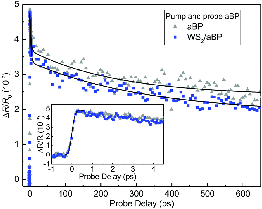 | ||
| Fig. 3 Time-resolved differential reflection measurements with a 1.55 eV pump and a 0.8 eV probe. The inset provides a closer look at the data near zero probe delay. | ||
The observation that WS2 does not introduce noticeable changes in the carrier dynamics in aBP is solid evidence that electrons excited in aBP cannot transfer to WS2 during their lifetime in aBP: If electrons could transfer from aBP to WS2, such an additional channel would cause a change of the signal. That is, the signal would have a fast-decay component, due to loss of electrons to WS2, followed by a very slow component due to the extended lifetime of the holes that are separated from the electrons. Since the signals from the two samples are very similar, we can conclude that electron transfer does not occur in the time scale studied.
The lack of electron transfer from aBP to WS2 indicates that although efficient charge transfer can occur from the crystalline to amorphous layers, the opposite transfer is inefficient. This can be attributed to the amorphous nature of aBP. Due to the lack of a long-range lattice, electron states in aBP are expected to be largely localized. The localization of the electron wavefunction can prohibit transfer to WS2 even if there are lower energy states available in WS2. It is also possible that aBP does not have a well-defined band edge, and hence there exist conduction band states below WS2.
3.4 Control of charge transfer by hBN
Having demonstrated the ultrafast hole transfer from WS2 to aBP and the lack of electron transfer from aBP to WS2, we next explored control of charge transfer by using a thin hBN barrier. We first exfoliated a thin hBN flake onto PDMS and then transferred it on top of aBP. Fig. 4(a) shows the green-channel microscope image of this flake, which clearly shows step-like contrasts with regions of 4.2% and 8.3%, as indicated in the figure. Previously, it has been shown that these contrasts correspond to monolayer and bilayer hBN flakes, respectively.61,62 We next transferred a WS2 ML flake partially on the bilayer hBN regions. The black triangles in Fig. 4(c) show the PL spectrum from part of the WS2 flake on bilayer hBN under 405 nm excitation. The main peak is slightly shifted to the low energy side compared to WS2/aBP (blue squares). Its peak is about 3 times higher than that of WS2/aBP, and is thus about 8 times lower than that of WS2 ML [Fig. 4(c)]. This feature shows that the bilayer hBN can slow down the hole transfer from WS2 to aBP despite its ultrasmall thickness. However, the quenching factor of 8 compared to WS2 ML shows that the hole transfer is still rather efficient. It is interesting to note that a new peak on the low-energy side of the main WS2 peak was observed in WS2/bilayer-hBN/aBP, whose origin is subject to further investigations.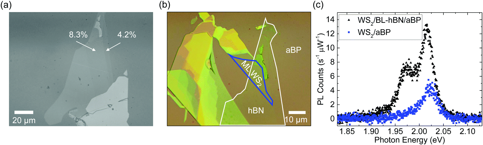 | ||
| Fig. 4 (a) The green-channel image of the hBN flake on aBP before the WS2 flake was transferred. The regions with contrasts of 4.2% and 8.3% are identified as monolayer and bilayer, respectively. (b) Optical microscope images of the sample after a WS2 monolayer was transferred partially on aBP and partially on the bilayer region of hBN. (c) Photoluminescence spectra of ML WS2 directly on aBP (blue symbols) and on bilayer hBN (black). | ||
4 Conclusions
In summary, we have shown that ultrafast and efficient charge transfer can occur from a monolayer crystal to an amorphous semiconducting ultrathin film. We have fabricated heterostructures of monolayer WS2 and 2 nm amorphous black phosphorus. Significant photoluminescence quenching of WS2 induced by the amorphous black phosphorus layer indicates efficient excitation transfer from WS2 to amorphous black phosphorus. The photocarrier dynamics in the heterostructure as well as the individual component layers of WS2 and amorphous black phosphorus were studied by transient absorption measurements in reflection geometry. By selectively pumping and probing each layer, we found evidence that holes injected in WS2 transfer to amorphous black phosphorus on an ultrashort time scale on the order of 100 fs or shorter. On the other hand, electrons in neither WS2 nor amorphous black phosphorus can transfer to the other layer. We attribute the lack of electron transfer from amorphous black phosphorus to WS2 to the localized nature of electronic states in amorphous materials. Furthermore, we show that a hBN bilayer can effectively change the hole transfer process. These results introduce amorphous black phosphorus as a building block for van der Waals heterostructures, reveal new information for understanding interlayer charge transfer, and provide a method to electrically connect to amorphous materials by van der Waals interfaces.Conflicts of interest
There are no conflicts to declare.Acknowledgements
This work was supported by the National Science Foundation of the USA (DMR-1505852) and the Research Grants Council of Hong Kong (Projects: PolyU 153271/16P and 153039/17P).References
- E. Gibney, Nature, 2015, 522, 274–276 CrossRef CAS PubMed.
- A. H. C. Neto and K. Novoselov, Rep. Prog. Phys., 2011, 74, 082501 CrossRef.
- Q. H. Wang, K. Kalantar-Zadeh, A. Kis, J. N. Coleman and M. S. Strano, Nat. Nanotechnol., 2012, 7, 699–712 CrossRef CAS PubMed.
- S. Z. Butler, S. M. Hollen, L. Cao, Y. Cui, J. A. Gupta, H. R. Gutiérrez, T. F. Heinz, S. S. Hong, J. Huang, A. F. Ismach, E. Johnston-Halperin, M. Kuno, V. V. Plashnitsa, R. D. Robinson, R. S. Ruoff, S. Salahuddin, J. Shan, L. Shi, M. G. Spencer, M. Terrones, W. Windl and J. E. Goldberger, ACS Nano, 2013, 7, 2898 CrossRef CAS PubMed.
- Z. Lin, A. McCreary, N. Briggs, S. Subramanian, K. H. Zhang, Y. F. Sun, X. F. Li, N. J. Borys, H. T. Yuan, S. K. Fullerton-Shirey, A. Chernikov, H. Zhao, S. McDonnell, A. M. Lindenberg, K. Xiao, B. J. LeRoy, M. Drndic, J. C. M. Hwang, J. Park, M. Chhowalla, R. E. Schaak, A. Javey, M. C. Hersam, J. Robinson and M. Terrones, 2D Mater., 2016, 3, 042001 CrossRef.
- A. K. Geim and I. V. Grigorieva, Nature, 2013, 499, 419–425 CrossRef CAS PubMed.
- Y. Liu, N. O. Weiss, X. Duan, H.-C. Cheng, Y. Huang and X. Duan, Nat. Rev. Mater., 2016, 1, 16042 CrossRef CAS.
- K. S. Novoselov, A. Mishchenko, A. Carvalho and A. H. C. Neto, Science, 2016, 353, 461 CrossRef CAS PubMed.
- W. J. Yu, Y. Liu, H. Zhou, A. Yin, Z. Li, Y. Huang and X. Duan, Nat. Nanotechnol., 2013, 8, 952–958 CrossRef CAS PubMed.
- D. D. Fazio, I. Goykhman, D. Yoon, M. Bruna, A. Eiden, S. Milana, U. Sassi, M. Barbone, D. Dumcenco, K. Marinov, A. Kis and A. C. Ferrari, ACS Nano, 2016, 10, 8252–8262 CrossRef PubMed.
- W. J. Yu, Q. A. Vu, H. Oh, H. G. Nam, H. L. Zhou, S. Cha, J. Y. Kim, A. Carvalho, M. Jeong, H. Choi, A. H. C. Neto, Y. H. Lee and X. F. Duan, Nat. Commun., 2016, 7, 13278 CrossRef CAS PubMed.
- L. Britnell, R. M. Ribeiro, A. Eckmann, R. Jalil, B. D. Belle, A. Mishchenko, Y.-J. Kim, R. V. Gorbachev, T. Georgiou, S. V. Morozov, A. N. Grigorenko, A. K. Geim, C. Casiraghi, A. H. C. Neto and K. S. Novoselov, Science, 2013, 340, 1311–1314 CrossRef CAS PubMed.
- S. V. Morozov, K. S. Novoselov, M. I. Katsnelson, F. Schedin, D. C. Elias, J. A. Jaszczak and A. K. Geim, Phys. Rev. Lett., 2008, 100, 016602 CrossRef CAS PubMed.
- H.-L. Liu, C.-C. Shen, S.-H. Su, C.-L. Hsu, M.-Y. Li and L.-J. Li, Appl. Phys. Lett., 2014, 105, 201905 CrossRef.
- M. H. Chiu, C. D. Zhang, H. W. Shiu, C. P. Chuu, C. H. Chen, C. Y. S. Chang, C. H. Chen, M. Y. Chou, C. K. Shih and L. J. Li, Nat. Commun., 2015, 6, 7666 CrossRef CAS PubMed.
- H. Fang, C. Battaglia, C. Carraro, S. Nemsak, B. Ozdol, J. S. Kang, H. A. Bechtel, S. B. Desai, F. Kronast, A. A. Unal, G. Conti, C. Conlon, G. K. Palsson, M. C. Martin, A. M. Minor, C. S. Fadley, E. Yablonovitch, R. Maboudian and A. Javey, Proc. Natl. Acad. Sci. U. S. A., 2014, 111, 6198–6202 CrossRef CAS PubMed.
- X. Hong, J. Kim, S. F. Shi, Y. Zhang, C. Jin, Y. Sun, S. Tongay, J. Wu, Y. Zhang and F. Wang, Nat. Nanotechnol., 2014, 9, 682–686 CrossRef CAS PubMed.
- F. Ceballos, M. Z. Bellus, H. Y. Chiu and H. Zhao, ACS Nano, 2014, 8, 12717–12724 CrossRef CAS PubMed.
- P. Rivera, J. R. Schaibley, A. M. Jones, J. S. Ross, S. Wu, G. Aivazian, P. Klement, K. Seyler, G. Clark, N. J. Ghimire, J. Yan, D. G. Mandrus, W. Yao and X. Xu, Nat. Commun., 2015, 6, 6242 CrossRef CAS PubMed.
- C. H. Lee, G. H. Lee, A. M. van der Zande, W. Chen, Y. Li, M. Han, X. Cui, G. Arefe, C. Nuckolls, T. F. Heinz, J. Guo, J. Hone and P. Kim, Nat. Nanotechnol., 2014, 9, 676–681 CrossRef CAS PubMed.
- P. Rivera, K. L. Seyler, H. Y. Yu, J. R. Schaibley, J. Q. Yan, D. G. Mandrus, W. Yao and X. D. Xu, Science, 2016, 351, 688–691 CrossRef CAS PubMed.
- J. R. Schaibley, P. Rivera, H. Y. Yu, K. L. Seyler, J. Q. Yan, D. G. Mandrus, T. Taniguchi, K. Watanabe, W. Yao and X. D. Xu, Nat. Commun., 2016, 7, 13747 CrossRef CAS PubMed.
- W. G. Xu, W. W. Liu, J. F. Schmidt, W. J. Zhao, X. Lu, T. Raab, C. Diederichs, W. B. Gao, D. V. Seletskiy and Q. H. Xiong, Nature, 2017, 541, 62 CrossRef CAS PubMed.
- A. T. Hanbicki, H.-J. Chuang, M. R. Rosenberger, C. S. Hellberg, S. V. Sivaram, K. M. McCreary, I. I. Mazin and B. T. Jonker, ACS Nano, 2018, 12, 4719–4726 CrossRef CAS PubMed.
- Y. Wang, Z. Wang, W. Yao, G. B. Liu and H. Y. Yu, Phys. Rev. B, 2017, 95, 115429 CrossRef.
- J. Sun, H. W. Lee, M. Pasta, H. T. Yuan, G. Y. Zheng, Y. M. Sun, Y. Z. Li and Y. Cui, Nat. Nanotechnol., 2015, 10, 980 CrossRef CAS PubMed.
- M. Q. Huang, S. M. Li, Z. F. Zhang, X. Xiong, X. F. Li and Y. Q. Wu, Nat. Nanotechnol., 2017, 12, 1148 CrossRef CAS PubMed.
- J. Shim, S. Oh, D. H. Kang, S. H. Jo, M. H. Ali, W. Y. Choi, K. Heo, J. Jeon, S. Lee, M. Kim, Y. J. Song and J. H. Park, Nat. Commun., 2016, 7, 13413 CrossRef CAS PubMed.
- D.-H. Kwak, H.-S. Ra, M.-H. Jeong, A.-Y. Lee and J.-S. Lee, Adv. Mater. Interfaces, 2018, 5, 1800671 CrossRef.
- F. Wang, Z. X. Wang, K. Xu, F. M. Wang, Q. S. Wang, Y. Huang, L. Yin and J. He, Nano Lett., 2015, 15, 7558–7566 CrossRef CAS PubMed.
- A. Vargas, F. Z. Liu, C. Lane, D. Rubin, I. Bilgin, Z. Hennighausen, M. DeCapua, A. Bansil and S. Kar, Sci. Adv., 2017, 3, e1601741 CrossRef PubMed.
- D. Zhong, K. L. Seyler, X. Y. Linpeng, R. Cheng, N. Sivadas, B. Huang, E. Schmidgall, T. Taniguchi, K. Watanabe, M. A. McGuire, W. Yao, D. Xiao, K. M. C. Fu and X. D. Xu, Sci. Adv., 2017, 3, e1603113 CrossRef PubMed.
- L. Niu, X. F. Liu, C. X. Cong, C. Y. Wu, D. Wu, T. R. Chang, H. Wang, Q. S. Zeng, J. D. Zhou, X. L. Wang, W. Fu, P. Yu, Q. D. Fu, S. Najmaei, Z. H. Zhang, B. I. Yakobson, B. K. Tay, W. Zhou, H. T. Jeng, H. Lin, T. C. Sum, C. Jin, H. Y. He, T. Yu and Z. Liu, Adv. Mater., 2015, 27, 7800–7808 CrossRef CAS PubMed.
- H. C. Cheng, G. M. Wang, D. H. Li, Q. Y. He, A. X. Yin, Y. Liu, H. Wu, M. N. Ding, Y. Huang and X. F. Duan, Nano Lett., 2016, 16, 367–373 CrossRef CAS PubMed.
- X. Liu, J. Gu, K. Ding, D. J. Fan, X. E. Hu, Y. W. Tseng, Y. H. Lee, V. Menon and S. R. Forrest, Nano Lett., 2017, 17, 3176–3181 CrossRef CAS PubMed.
- Y. Huang, F. W. Zhuge, J. X. Hou, L. Lv, P. Luo, N. Zhou, L. Gan and T. Y. Zhai, ACS Nano, 2018, 12, 4062–4073 CrossRef CAS PubMed.
- T. Kafle, B. Kattel, S. D. Lane, T. Wang, H. Zhao and W. L. Chan, ACS Nano, 2017, 11, 10184–10192 CrossRef CAS PubMed.
- A. Shah, P. Torres, R. Tscharner, N. Wyrsch and H. Keppner, Science, 1999, 285, 692–698 CrossRef CAS PubMed.
- P. G. Lecomber, W. E. Spear and A. Ghaith, Electron. Lett., 1979, 15, 179–181 CrossRef CAS.
- K. Nomura, H. Ohta, A. Takagi, T. Kamiya, M. Hirano and H. Hosono, Nature, 2004, 432, 488–492 CrossRef CAS PubMed.
- K. S. Suslick, S. B. Choe, A. A. Cichowlas and M. W. Grinstaff, Nature, 1991, 353, 414–416 CrossRef CAS.
- R. D. L. Smith, M. S. Prevot, R. D. Fagan, Z. P. Zhang, P. A. Sedach, M. K. J. Siu, S. Trudel and C. P. Berlinguette, Science, 2013, 340, 60–63 CrossRef CAS PubMed.
- Z. Yang, J. Hao, S. Yuan, S. Lin, H. M. Yau, J. Dai and S. P. Lau, Adv. Mater., 2015, 27, 3748–3754 CrossRef CAS PubMed.
- Y. Z. Guo and J. Robertson, Appl. Phys. Lett., 2016, 108, 233104 CrossRef.
- Y. Cai, G. Zhang and Y. W. Zhang, Sci. Rep., 2014, 4, 6677 CrossRef CAS PubMed.
- Z. Ye, T. Cao, K. O'Brien, H. Zhu, X. Yin, Y. Wang, S. G. Louie and X. Zhang, Nature, 2014, 513, 214–218 CrossRef CAS PubMed.
- B. Zhu, H. Zeng, J. Dai, Z. Gong and X. Cui, Proc. Natl. Acad. Sci. U. S. A., 2014, 111, 11606–11611 CrossRef CAS PubMed.
- W. J. Zhao, Z. Ghorannevis, L. Q. Chu, M. L. Toh, C. Kloc, P. H. Tan and G. Eda, ACS Nano, 2013, 7, 791–797 CrossRef CAS PubMed.
- N. Peimyoo, J. Z. Shang, C. X. Cong, X. N. Shen, X. Y. Wu, E. K. L. Yeow and T. Yu, ACS Nano, 2013, 7, 10985–10994 CrossRef CAS PubMed.
- F. Ceballos, Q. Cui, M. Z. Bellus and H. Zhao, Nanoscale, 2016, 8, 11681–11688 RSC.
- C. Mai, Y. G. Semenov, A. Barrette, Y. F. Yu, Z. H. Jin, L. Y. Cao, K. W. Kim and K. Gundogdu, Phys. Rev. B: Condens. Matter Mater. Phys., 2014, 90, 041414 CrossRef.
- J. He, D. He, Y. Wang, Q. Cui, F. Ceballos and H. Zhao, Nanoscale, 2015, 7, 9526 RSC.
- M. Z. Bellus, Z. B. Yang, J. H. Hao, S. P. Lau and H. Zhao, 2D Mater., 2017, 4, 025063 CrossRef.
- F. J. M. Hoeben, P. Jonkheijm, E. W. Meijer and A. Schenning, Chem. Rev., 2005, 105, 1491–1546 CrossRef CAS PubMed.
- D. L. Dexter, J. Chem. Phys., 1953, 21, 836–850 CrossRef CAS.
- C. B. Murphy, Y. Zhang, T. Troxler, V. Ferry, J. J. Martin and W. E. Jones, J. Phys. Chem. B, 2004, 108, 1537–1543 CrossRef CAS.
- F. Ceballos, M. Z. Bellus, H. Y. Chiu and H. Zhao, Nanoscale, 2015, 7, 17523–17528 RSC.
- B. Peng, G. Yu, X. Liu, B. Liu, X. Liang, L. Bi, L. Deng, T. C. Sum and K. P. Loh, 2D Mater., 2016, 3, 025020 CrossRef.
- H. M. Zhu, J. Wang, Z. Z. Gong, Y. D. Kim, J. Hone and X. Y. Zhu, Nano Lett., 2017, 17, 3591–3598 CrossRef CAS PubMed.
- S. J. Haigh, A. Gholinia, R. Jalil, S. Romani, L. Britnell, D. C. Elias, K. S. Novoselov, L. A. Ponomarenko, A. K. Geim and R. Gorbachev, Nat. Mater., 2012, 11, 764–767 CrossRef CAS PubMed.
- D. Golla, K. Chattrakun, K. Watanabe, T. Taniguchi, B. J. LeRoy and A. Sandhu, Appl. Phys. Lett., 2013, 102, 161906 CrossRef.
- R. Gorbachev, I. Riaz, R. Nair, R. Jalil, L. Britnell, B. Belle, E. Hill, K. Novoselov, K. Watanabe, T. Taniguchi, A. Geim and P. Blake, Small, 2011, 7, 465–468 CrossRef CAS PubMed.
Footnote |
| † Electronic supplementary information (ESI) available. See DOI: 10.1039/c8nh00234g |
| This journal is © The Royal Society of Chemistry 2019 |