
Copper(I) sulfide: a two-dimensional semiconductor with superior oxidation resistance and high carrier mobility†
Yu
Guo‡
ab,
Qisheng
Wu‡
bc,
Yunhai
Li
c,
Ning
Lu
d,
Keke
Mao
be,
Yizhen
Bai
a,
Jijun
Zhao
*a,
Jinlan
Wang
 *cf and
Xiao Cheng
Zeng
*bg
*cf and
Xiao Cheng
Zeng
*bg
aKey Laboratory of Materials Modification by Laser, Ion and Electron Beams (Dalian University of Technology), Ministry of Education, Dalian, Liaoning 116024, China. E-mail: zhaojj@dlut.edu.cn
bDepartment of Chemistry, University of Nebraska–Lincoln, Lincoln, Nebraska 68588, USA. E-mail: xzeng1@unl.edu
cSchool of Physics, Southeast University, Nanjing, Jiangsu 211189, China. E-mail: jlwang@seu.edu.cn
dAnhui Province Key Laboratory of Optoelectric Materials Science and Technology, Department of Physics, Anhui Normal University, Wuhu, Anhui 241000, China
eSchool of Energy and Environment Science, Anhui University of Technology, Maanshan, Anhui 243032, China
fSynergetic Innovation Center for Quantum Effects and Applications (SICQEA), Hunan Normal University, Changsha, Hunan 410081, China
gDepartment of Chemical & Biomolecular Engineering and Department of Mechanical & Materials Engineering, University of Nebraska–Lincoln, Lincoln, Nebraska 68588, USA
First published on 19th September 2018
Abstract
Two-dimensional (2D) semiconductors with suitable direct band gaps, high carrier mobility, and excellent open-air stability are especially desirable for material applications. Herein, we show theoretical evidence of a new phase of a copper(I) sulfide (Cu2S) monolayer, denoted δ-Cu2S, with both novel electronic properties and superior oxidation resistance. We find that both monolayer and bilayer δ-Cu2S have much lower formation energy than the known β-Cu2S phase. Given that β-Cu2S sheets have been recently synthesized in the laboratory (Adv. Mater.2016, 28, 8271), the higher stability of δ-Cu2S than that of β-Cu2S sheets suggests a high possibility of experimental realization of δ-Cu2S. Stability analysis indicates that δ-Cu2S is dynamically and thermally stable. Notably, δ-Cu2S exhibits superior oxidation resistance, due to the high activation energy of 1.98 eV for the chemisorption of O2 on δ-Cu2S. On its electronic properties, δ-Cu2S is a semiconductor with a modest direct band gap (1.26 eV) and an ultrahigh electron mobility of up to 6880 cm2 V−1 s−1, about 27 times that (246 cm2 V−1 s−1) of the β-Cu2S bilayer. The marked difference between the electron and hole mobilities of δ-Cu2S suggests easy separation of electrons and holes for solar energy conversion. Combination of these novel properties makes δ-Cu2S a promising 2D material for future applications in electronics and optoelectronics with high thermal and chemical stability.
Conceptual insightsCopper sulfides have been extensively studied owing to their high abundance, easy preparation, and outstanding chemical and physical properties. Here we report a hitherto unreported 2D copper(I) sulfide, namely, a δ-Cu2S monolayer. The δ-Cu2S monolayer is a semiconductor with a desirable direct band gap of 1.26 eV, close to that of bulk silicon, as well as a high electron mobility of up to 6880 cm2 V−1 s−1, about 27 times that of the β-Cu2S bilayer (246 cm2 V−1 s−1, measured value). Unlike many other 2D modest-band-gap semiconductors which have relatively low chemical stability, notably, the δ-Cu2S monolayer exhibits superior oxidation resistance, as demonstrated by the high activation energy of 1.98 eV for the chemisorption of O2 on δ-Cu2S. Another novel feature of the δ-Cu2S solid is that it has much lower formation energy than the previously known β-Cu2S solid, suggesting a high likelihood of achieving a δ-Cu2S monolayer in the laboratory. |
Introduction
Copper sulfide (Cu2−xS, 0 ≤ x ≤ 1) nanomaterials have been extensively studied owing to their high abundance, easy preparation, and excellent chemical and physical properties.1–4 In the laboratory, Cu2−xS can be synthesized using various methods, e.g., the colloidal solution process, the wet chemical method, and the facile solvothermal method.5–8 Among many Cu2−xS nanomaterials, Cu2S (chalcocite) is known for its excellent optical and electronic properties with potential applications in lithium storage,9 high-capacity cathode materials in lithium secondary batteries,10 photocatalysts,11 and absorbers in photovoltaic conversions.12–14 Bulk Cu2S solids are usually classified as α (stable above 425 °C), β (high chalcocite; stable between 105 and 425 °C) and γ (low chalcocite; the first solid–liquid hybrid phase, and stable below 105 °C) phases,15 respectively. Phase transition between the high and low chalcocite phases could be achieved by heating with an electron beam at relatively low temperature.5,16,17Two-dimensional (2D) materials have attracted extensive attention due largely to many of their novel properties which are not seen in their bulk counterparts.18–23 Very recently, 2D β-Cu2S sheets with thicknesses down to 1.8 nm have been synthesized and proven to exist as a hybrid solid–liquid phase.8,24,25 The temperature (−15 °C) for high chalcocite to low chalcocite transition is much lower than that of the bulk counterpart (105 °C), rendering 2D β-Cu2S sheets available for room-temperature applications.8 Similarly, the transition temperature from β-Cu2S to γ-Cu2S also decreases with decreasing nanoparticle size.26 In addition, Cu2S sheets exhibit higher photo-activity for solar energy conversion than their bulk counterpart.27 A previous theoretical calculation predicted that a β-Cu2S bilayer is the thinnest stable layer as the two layers are strongly bonded, evidenced by the large binding energy between the layers (0.93 eV per Cu2S unit).24 Moreover, the β-Cu2S bilayer exhibits a direct band gap of 0.9 eV at the high-symmetry point Γ,8 implying that the β-Cu2S bilayer could be a promising candidate for electronic and optical applications.
Although the solid–liquid phase is quite interesting,8,15,24 it also indicates meta-stability and rapid diffusion of atoms, which may degrade the material's performance. In this article, we predict a new phase of a Cu2S monolayer, denoted δ-Cu2S, based on global structural search and first-principles calculations. Our computation indicates that the δ-Cu2S monolayer and bilayer are semiconductors with modest direct band gaps and ultrahigh electron mobilities of up to 6880 cm2 V−1 s−1 and 5786 cm2 V−1 s−1, respectively. The latter is more than one order of magnitude higher than that of the bilayer β phase (246 cm2 V−1 s−1). Our computation also shows that δ-Cu2S is dynamically and thermally stable, and chemically inert upon oxidation. In particular, the superior oxidation resistance of δ-Cu2S, due to the high activation energy (1.98 eV) for the chemisorption of O2 on this 2D sheet, is the distinct feature compared with many ultrathin 2D materials with poor chemical stability in open air.28–31 A well-known example is black phosphorus whose 2D counterpart – phosphorene – is hydrophilic and can be easily oxidized in air moisture with a low activation energy of 0.70 eV.32 Oxidation of phosphorene leads to higher contact resistance, lower carrier mobility, and possible mechanical degradation and breakdown.29,32,33
Results and discussion
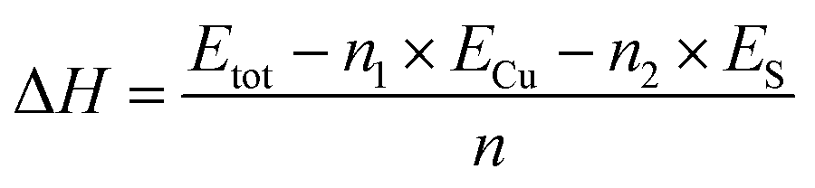
After a systematic structural search, hundreds of structures were generated using the CALYPSO code. Four representative low-lying structures are shown in Fig. S1 (ESI†), and their stability analyses are presented in Fig. S2 and Table S1 (ESI†). The δ-Cu2S monolayer is identified as the most stable 2D structure. Fig. 1a presents the optimized structure of δ-Cu2S, with a tetragonal structure and lateral isotropy. The unit cell of δ-Cu2S has four Cu and two S atoms, with each Cu atom being bonded with five Cu atoms and two S atoms, and each S atom being bonded with four Cu atoms. As shown in Fig. 1a, the optimized 2D layered structure has a lattice constant (a) of 5.02 Å and a thickness (h) of 2.55 Å along the z direction, with average Cu–S and Cu–Cu bond lengths of 2.22 Å and 2.57 Å, respectively (see Table 1). To gain insight into the chemical bond of δ-Cu2S, we calculated the electron localization function (ELF).34–36 As displayed in Fig. 1b, the electrons are mainly localized around S atoms and absent in the middle region between Cu and S atoms, indicating the distinct feature of ionic bonding. In addition, Bader charge analysis37,38 shows a substantial number of electrons, i.e., 0.32 e donated from each Cu atom to S atoms (Table 1).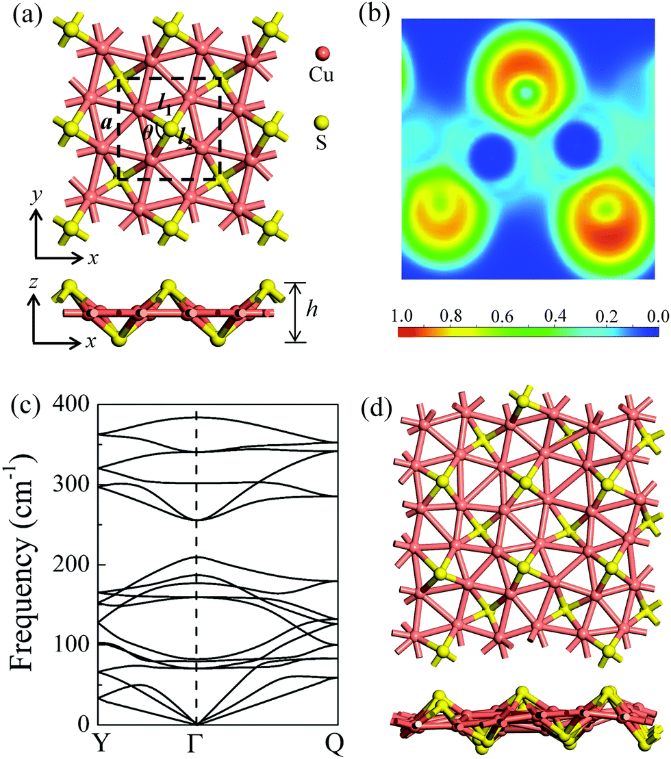 | ||
| Fig. 1 (a) The atomic structures of δ-Cu2S from top and side views, respectively. The unit cell is denoted by dashed lines. a, l1, l2, θ and h represent the lattice constant, the Cu–Cu and Cu–S bond lengths, the Cu–S–Cu bond angle, and the layer thickness along the z direction, respectively. (b) Electron localization functions (ELFs); ELF = 1 (red) and 0 (blue) indicate the accumulated and vanishing electron densities, respectively. (c) Phonon dispersion of δ-Cu2S. High-symmetry points of the first Brillouin zone are Y (0, 0.5, 0), Γ (0, 0, 0) and Q (0.5, 0.5, 0), as shown in Fig. 4b. (d) Snapshots of the equilibrium structures of the Cu2S monolayer at 800 K after 10 ps ab initio molecular dynamics simulation. Cu and S atoms are shown in pink and yellow colors, respectively. | ||
| a (Å) | l 1 (Å) | l 2 (Å) | θ (°) | h (Å) | Q Cu (e) |
|---|---|---|---|---|---|
| 5.02 | 2.57 | 2.22 | 70.76 | 2.55 | 0.32 |
| Material | Carrier type | m (m0) | E 1 (eV) | C (J m−2) | μ (cm2 V−1 s−1) |
|---|---|---|---|---|---|
| δ-Monolayer | Holes | 4.28 | 1.79 | 40.59 | 14.54 |
| Electrons | 0.21 | 1.71 | 40.59 | 6880.17 | |
| δ-Bilayer | Holes | 0.23 | 4.28 | 94.99 | 2107.74 |
| Electrons | 0.16 | 3.66 | 94.99 | 5786.28 | |
| β-Bilayer (armchair) | Holes | 0.98 | 4.79 | 63.99 | 79.68 |
| Electrons | 0.49 | 5.07 | 63.99 | 222.09 | |
| β-Bilayer (zigzag) | Holes | 0.59 | 5.00 | 65.78 | 109.37 |
| Electrons | 0.47 | 5.35 | 65.78 | 246.51 | |
To evaluate the energetic stability of δ-Cu2S, we first calculated the formation energy ΔH defined as
 | (1) |
Since the experimentally synthesized δ-Cu2S sheets could be multilayer rather than monolayer, we also considered several high-symmetry stacking configurations for δ-Cu2S monolayers. We found that the AA stacking in Fig. 4b is the most stable bilayer configuration with an interlayer binding energy of −0.08 eV per atom, comparable with that of graphene and phosphorene (around −0.06 eV per atom) bilayers.39,40 According to eqn (1), the formation energy (−0.13 eV per atom) for the δ-Cu2S bilayer is also much lower than that of the β-Cu2S bilayer, again suggesting the likelihood of the synthesis of the δ-Cu2S bilayer.
The dynamic stability of δ-Cu2S is confirmed by the absence of imaginary frequencies in computed phonon dispersion (Fig. 1c). We also performed Born–Oppenheimer molecular dynamics (BOMD) simulations to examine the thermal stability of the 2D structure at elevated temperature. The BOMD simulations show that the δ-Cu2S monolayer can maintain its structural integrity even up to 800 K for 10 ps (Fig. 1d), indicating its exceeding stability even above room temperature. At a temperature of 900 K, the planar structure is highly distorted within 10 ps of BOMD simulation (Fig. S4d, ESI†). Furthermore, for both Cu and S atoms, we calculated the mean-square-diffusion distance,8 defined as 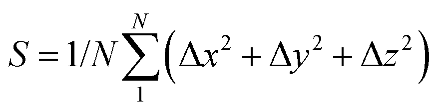 , where N is the number of atoms for each element, and Δx, Δy and Δz are the differences of Cartesian coordinates for the same atom at the beginning and end of the BOMD simulation. As shown in Fig. 2, the mean-square-diffusion distances for Cu and S atoms remain almost unchanged with time t. At a temperature of 800 K, the S atoms diffuse a bit more than the Cu atoms since the Cu atoms are covered by the S atoms (see Fig. 1a). The computed time-dependent mean-square-diffusion distances of the Cu and S atoms indicate that the δ-Cu2S monolayer is still in the solid phase at 800 K, contrary to the hybrid solid–liquid phase of bulk β-Cu2S at room temperature.8 This result further supports that the δ-Cu2S monolayer exhibits higher structural stability than the β-Cu2S monolayer at room temperature.
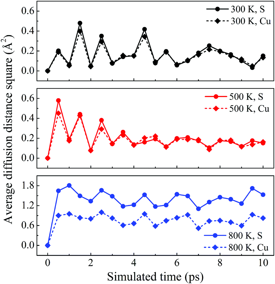 | ||
| Fig. 2 Average diffusion distance squares as functions of simulated time for δ-Cu2S at 300 K, 500 K and 800 K from top to bottom panels, respectively. | ||
To examine the chemical stability of the δ-Cu2S monolayer in an open-air environment, we investigated the physisorption and chemisorption of an O2 molecule on the surface of a 2D sheet, and computed the dissociative oxidation pathway. The interaction between O2 and the monolayer is described by the binding energy (Ebind) defined as follows:
| Ebind = Etot − Eδ − EO2 | (2) |
Fig. 3 illustrates the adsorption configurations and dissociation process for an O2 molecule, initially physisorbed on the δ-Cu2S, turning into two oxygen atoms chemisorbed on the monolayer. In the initial stage of physisorption, the O2 molecule is located about 3.7 Å above the surface of δ-Cu2S with a binding energy of −0.09 eV. As the O2 molecule approaches the 2D sheet, the O–O bond is elongated to 1.65 Å in the transition state. The O2 molecule undergoes a transition from physisorption to chemisorption by overcoming an activation energy (Ea) of 1.98 eV, suggesting an extremely slow oxidation rate at room temperature. This activation energy is even greater than that calculated for a MoS2 monolayer (1.59 eV),41 which already exhibits relatively high resistance to O2 chemisorption. Thus, the δ-Cu2S monolayer is expected to be a superior oxidation-resistant material, as the MoS2 monolayer. Note that we considered several other adsorption sites for O2 and selected the initial and final structures with the lowest binding energy to simulate the oxidation process of δ-Cu2S (see S4 (ESI†) for details).
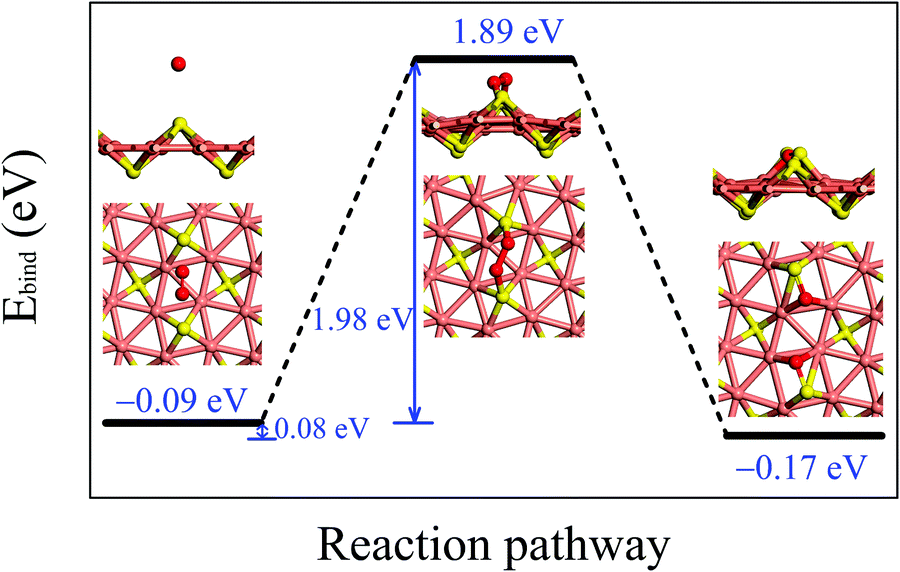 | ||
| Fig. 3 Reaction pathway for an O2 molecule to dissociate into two O atoms on the δ-Cu2S monolayer. The black line segments indicate the energy levels of the initial, transition, and final states, respectively, with the corresponding atomic structures (top and side views) given next to the energy levels. The blue numbers give (from left to right) the binding energy of the initial state, the heat of reaction, the activation energy, and the binding energies of the transition and final states, respectively. The O, S and Cu atoms are painted in red, yellow and pink, respectively. | ||
The bonding energy of O2 is often overestimated by DFT/PBE calculations. If we adopt the experimental value of O2 bonding energy (5.16 eV)42 instead of the DFT value, the binding energy (Ebind*) could be redefined as:
| Ebind* = Etot − Eδ − 2 × EO − Ebond | (3) |
To characterize the thermal stability of the oxidized products, we defined the heat of reaction as follows:
| EH = Ephysbind − Echembind | (4) |
The electronic band structure and local density of states (LDOS) of the δ-Cu2S monolayer were computed using the HSE06 functional (Fig. 4a). The HSE06 computation suggests that δ-Cu2S possesses a modest direct band gap of 1.26 eV at the Γ point, 0.24 eV smaller than the HSE06 bandgap of 1.50 eV for bilayer β-Cu2S (Fig. S3, ESI†). The LDOS analysis reveals that the edges of the valence bands are dominated by the 3d orbitals of the Cu atoms, while the conduction band edges stem mainly from the 3d orbitals of the Cu atoms and partially from the 3p orbitals of the S atoms. Hence, the Cu atoms make the major contribution to both the valence band maximum (VBM) and the conduction band minimum (CBM). Meanwhile, the substantial overlap of the LDOS near the Fermi level implies strong hybridization between the orbitals of the Cu and S atoms. The computed carrier effective masses are 4.28 m0 for holes and 0.21 m0 for electrons, respectively. The relatively small effective mass of the electrons suggests that the carriers are rather mobile in the 2D sheet. Moreover, the large difference in effective masses can be exploited to separate the electrons and holes for solar energy conversion.
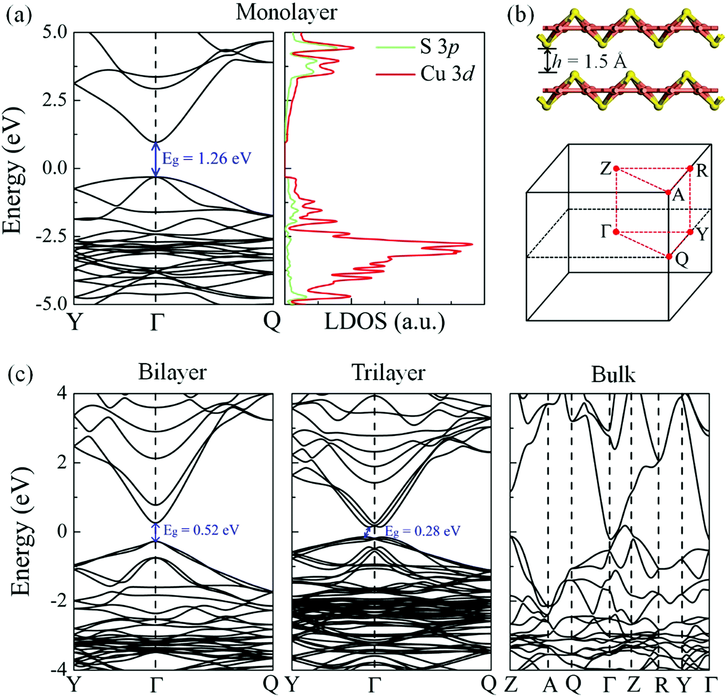 | ||
| Fig. 4 (a) Electronic band structure (left panel) and local density of states (LDOS, right panel) of the monolayer δ-Cu2S sheet. Green and red lines in LDOS represent contributions from S 3p and Cu 3d states, respectively. (b) Atomic structure of the layers of δ-Cu2S and Brillouin zone of the bulk counterpart. (c) Electronic band structures of bilayer, trilayer and bulk δ-Cu2S, respectively. Eg is the band gap denoted by a solid arrow. The Fermi levels are set to zero. | ||
Strain engineering offers a useful way to tune the electronic properties and performance of 2D atomic crystals. For example, a linear decrease in the optical band gap of MoS2 with strain has been experimentally confirmed via photoluminescence.43,44 To examine the strain effect on the band gap of the δ-Cu2S monolayer, we computed the electronic band structures of the δ-Cu2S monolayer under various biaxial strains up to ±3% (see Fig. S7 (ESI†) for details). The results indicate that the band gap of the δ-Cu2S monolayer linearly increases from 1.07 eV to 1.55 eV under a strain of −3% to 3%, which is similar to the strain effect on MoS2. The direct character and dispersion (see Fig. S7 and S8, ESI†) are preserved. For the multilayered system, as the layer thickness increases, the band gap decreases monotonically. Consequently, the δ-Cu2S bilayer and trilayer preserve the semiconducting behavior, with band gaps of 0.52 eV (direct) and 0.28 eV (indirect), while bulk δ-Cu2S is metallic. Furthermore, the δ-Cu2S bilayer possesses much smaller carrier effective masses of 0.23 m0 for holes and 0.16 m0 for electrons, compared with those of the β-Cu2S bilayer (0.56–0.98 m0 for holes and 0.47–0.49 m0 for electrons), as listed in Table 1, implying easy transport of carriers in the δ-Cu2S bilayer.
To further characterize the electron transport properties of the δ-Cu2S monolayer, we calculated their acoustic phonon-limited carrier mobility μ, based on the Takagi model within the deformation potential approximation:45–47
 | (5) |
 is the average effective mass (m⊥ is the effective mass perpendicular to the transport direction), and C2D is the elastic modulus of the 2D sheet, determined by the lattice parameter l along the transport direction via ΔE/S0 = C2D(Δl/l)2/2 (ΔE is the energy change of the system under lattice deformation Δl, and S0 is the area of unit cell). The term E1 represents the deformation potential constant of the VBM for a hole, or the CBM for an electron along the transport direction, defined by ΔV/(Δl/l) (ΔV is the band edge shift under lattice deformation). All data are calculated using a strain step of 0.5%. The temperature used in the mobility calculations is 300 K. The present carrier mobility calculation has been demonstrated to be physically reasonable and computationally efficient.48–50
As listed in Table 1, the electron mobility of the δ-Cu2S monolayer can reach as high as 6880 cm2 V−1 s−1, about five times that of phosphorene (1140 cm2 V−1 s−1).48 Its high carrier mobility is attributed to its small effective mass, large elastic modulus, and small deformation potential constant. The δ-Cu2S monolayer shows C2D values up to 40.59 J m−2, larger than that of phosphorene (28.94 J m−2 along the armchair direction),48 resulting in small-amplitude lattice waves and weak scattering with charge carriers. The deformation potential constant E1 is another important factor for carrier mobility. It approximately describes the strength of electron–phonon coupling and is determined by the band edge shift under lattice variation due to acoustic phonons. Here, E1 is as low as 1.71 eV, contributing to the ultra-high carrier mobility. The high electron mobility demonstrates that the δ-Cu2S monolayer is a good candidate for 2D electronic devices. Furthermore, the carrier mobility of electrons is three orders of magnitude larger than that of holes (14 cm2 V−1 s−1). The substantial difference between the transport behavior of electrons and holes could be beneficial to controlling the carrier transport, and separating the carriers to promote the device performance. More importantly, the electron mobility of the δ-Cu2S bilayer is as high as 5786 cm2 V−1 s−1, about 25 times that of the β-Cu2S bilayer (222 cm2 V−1 s−1 along the armchair direction and 246 cm2 V−1 s−1 along the zigzag direction). The high mobility of the δ-Cu2S bilayer also stems from the small carrier effective masses (∼0.16 m0), relatively small deformation potential constant (∼3.03 eV), and large elastic modulus (∼95 J m−2). The hole mobility of the δ-Cu2S bilayer (up to 2107 cm2 V−1 s−1) is notably higher than that of the monolayer counterpart as well as that (79–109 cm2 V−1 s−1) of the β-Cu2S bilayer. Therefore, the δ-Cu2S monolayer and bilayer exhibit more prominent carrier transport properties than the β-Cu2S bilayer, making layered δ-Cu2S a very promising candidate for future applications in electronic devices.
Conclusions
We have predicted a new phase of a Cu2S monolayer (δ-Cu2S) and explored its atomic structure, bonding character, structural, thermal and chemical stabilities, and electronic properties. In particular, δ-Cu2S sheets are energetically more favorable than recently synthesized 2D β-Cu2S sheets, and exhibit excellent dynamical and thermal stabilities. Importantly, the dissociation and chemisorption of O2 on δ-Cu2S are kinetically hampered by the relatively high activation energy of 1.98 eV, suggesting that δ-Cu2S can better withstand oxidation in ambient air. δ-Cu2S has a modest direct band gap of 1.26 eV, and an ultrahigh electron mobility of up to 6880 cm2 V−1 s−1. The large difference between the electron and hole mobilities can be valuable for the efficient separation of electrons and holes for solar conversion applications. Furthermore, the δ-Cu2S bilayer possesses lower formation energy and much higher carrier mobility (∼5786 cm2 V−1 s−1) than the β-Cu2S bilayer. Given that the β-Cu2S sheets have been recently synthesized in the laboratory, it is expected that δ-Cu2S sheets can be fabricated in the near future. In view of the combination of their novel electronic properties and superior oxidation resistance, δ-Cu2S sheets may play an even more important role in future 2D electronic devices than β-Cu2S sheets.Computational methods
First-principles calculations were performed using the Vienna ab initio simulation package (VASP 5.4),51 with the plane-wave basis set with an energy cutoff of 500 eV, the projector augmented wave potentials (PAW),52,53 and the generalized gradient approximation parameterized by Perdew, Burke and Ernzerhof (GGA-PBE) for the exchange–correlation functional.54 The convergence criteria for total energy and residual force on each atom were set to 10−7 eV and 0.01 eV Å−1, respectively. For a unit cell of a 2D δ-Cu2S system, the Brillouin zone was sampled with a Γ-centered 16 × 16 × 1 Monkhorst−Pack55k-point grid. Note that the standard GGA functional tends to underestimate the band gaps; thus a hybrid functional (HSE06)56 was also used to compute the electronic band structures of δ-Cu2S. The climbing-image nudged elastic band (CI-NEB) method57 was employed to investigate the adsorption kinetics of the O2 molecule, and to determine the activation energy for chemisorption. To this end, a 3 × 3 × 1 supercell containing 18 S atoms and 36 Cu atoms was built. Five images were used to calculate the reaction path. The intermediate image of each CI-NEB simulation was relaxed until the perpendicular forces were less than 0.02 eV Å−1. The DFT-D3 method58 was used to take into account the long-range van der Waals (vdW) interactions in the O2 adsorption and layered systems.To examine the dynamical stability of the δ-Cu2S monolayer, phonon dispersion was computed using the Phonopy code based on the density functional perturbation theory (DFPT)59 as incorporated with VASP. The Born–Oppenheimer molecular dynamics (BOMD) simulations with the PAW method and the PBE functional were carried out to assess the thermal stabilities of the predicted δ-Cu2S. In the BOMD simulations, the initial configuration of δ-Cu2S with a 3 × 3 × 1 supercell was annealed at several temperatures. Each BOMD simulation in the NVT ensemble lasted for 10 ps with a time step of 1.0 fs, and the temperature was controlled using the Nosé–Hoover method.59
The particle-swarm optimization (PSO) method implemented in the CALYPSO code60,61 was employed to search for low-energy structures of 2D (Cu2S)n (n = 1–4) monolayer sheets. As an unbiased global optimization method, the PSO algorithm has successfully predicted a variety of 2D structures with high stability.62–67 In our PSO search, both the population size and the number of generation were set to 30. The required structural relaxations were performed using the PBE functional, as implemented in the VASP 5.4 code.51
Conflicts of interest
There are no conflicts to declare.Acknowledgements
This work was supported by the National Natural Science Foundation of China (11574040, 21525311, 21373045, 21773027, 21403005, 21803002), the Fundamental Research Funds for the Central Universities of China (DUT16LAB01, DUT17LAB19), the National Key Research and Development Program of China (No. 2017YFA0204800), and the Jiangsu 333 project (BRA2016353). Y. G. is supported by the China Scholarship Council (CSC, 201706060138). Q. W. is supported by CSC (201606090079) and the Scientific Research Foundation of Graduate School of Southeast University (YBJJ1720). X. C. Z. is supported by the National Science Foundation (NSF) through the Nebraska Materials Research Science and Engineering Center (MRSEC) (Grant No. DMR-1420645). We acknowledge the computing resource from the Supercomputing Center of Dalian University of Technology, the University of Nebraska Holland Computing Center and the National Supercomputing Center in Tianjin.References
- Y. Xie, L. Carbone, C. Nobile, V. Grillo, S. D’Agostino, F. Della Sala, C. Giannini, D. Altamura, C. Oelsner, C. Kryschi and P. D. Cozzoli, ACS Nano, 2013, 7, 7352–7369 CrossRef CAS PubMed.
- J. M. Luther, P. K. Jain, T. Ewers and A. P. Alivisatos, Nat. Mater., 2011, 10, 361 CrossRef CAS PubMed.
- S.-W. Hsu, K. On and A. R. Tao, J. Am. Chem. Soc., 2011, 133, 19072–19075 CrossRef CAS PubMed.
- Y. Zhao, H. Pan, Y. Lou, X. Qiu, J. Zhu and C. Burda, J. Am. Chem. Soc., 2009, 131, 4253–4261 CrossRef CAS PubMed.
- H. Zheng, J. B. Rivest, T. A. Miller, B. Sadtler, A. Lindenberg, M. F. Toney, L.-W. Wang, C. Kisielowski and A. P. Alivisatos, Science, 2011, 333, 206 CrossRef CAS PubMed.
- S. He, G.-S. Wang, C. Lu, J. Liu, B. Wen, H. Liu, L. Guo and M.-S. Cao, J. Mater. Chem. A, 2013, 1, 4685–4692 RSC.
- B. Zhao, G. Shao, B. Fan, W. Zhao, Y. Xie and R. Zhang, J. Mater. Chem. A, 2015, 3, 10345–10352 RSC.
- B. Li, L. Huang, G. Zhao, Z. Wei, H. Dong, W. Hu, L.-W. Wang and J. Li, Adv. Mater., 2016, 28, 8271–8276 CrossRef CAS PubMed.
- R. Cai, J. Chen, J. Zhu, C. Xu, W. Zhang, C. Zhang, W. Shi, H. Tan, D. Yang, H. H. Hng, T. M. Lim and Q. Yan, J. Phys. Chem. C, 2012, 116, 12468–12474 CrossRef CAS.
- F. Han, W.-C. Li, D. Li and A.-H. Lu, ChemElectroChem, 2014, 1, 733–740 CrossRef CAS.
- Y. Kim, K. Y. Park, D. M. Jang, Y. M. Song, H. S. Kim, Y. J. Cho, Y. Myung and J. Park, J. Phys. Chem. C, 2010, 114, 22141–22146 CrossRef CAS.
- R. L. N. Chandrakanthi and M. A. Careem, Thin Solid Films, 2002, 417, 51–56 CrossRef CAS.
- G. Liu, T. Schulmeyer, J. Brötz, A. Klein and W. Jaegermann, Thin Solid Films, 2003, 431-432, 477–482 CrossRef CAS.
- M. Ashry and S. A. Fayek, Renewable Energy, 2001, 23, 441–450 CrossRef CAS.
- L.-W. Wang, Phys. Rev. Lett., 2012, 108, 085703 CrossRef PubMed.
- S.-H. Lee, Y. Jung and R. Agarwal, Nat. Nanotechnol., 2007, 2, 626 CrossRef CAS PubMed.
- M. H. R. Lankhorst, B. W. S. M. M. Ketelaars and R. A. M. Wolters, Nat. Mater., 2005, 4, 347 CrossRef CAS PubMed.
- K. S. Novoselov, A. K. Geim, S. V. Morozov, D. Jiang, Y. Zhang, S. V. Dubonos, I. V. Grigorieva and A. A. Firsov, Science, 2004, 306, 666 CrossRef CAS PubMed.
- Y. Liu, N. O. Weiss, X. Duan, H.-C. Cheng, Y. Huang and X. Duan, Nat. Rev. Mater., 2016, 1, 16042 CrossRef CAS.
- M. Xu, T. Liang, M. Shi and H. Chen, Chem. Rev., 2013, 113, 3766–3798 CrossRef CAS PubMed.
- M. Li, J. Dai and X. C. Zeng, Nanoscale, 2015, 7, 15385–15391 RSC.
- Y. Hong, J. Zhang and X. C. Zeng, Nanoscale, 2018, 10, 4301–4310 RSC.
- L. Ma, M.-G. Ju, J. Dai and X. C. Zeng, Nanoscale, 2018, 10, 11314–11319 RSC.
- F. B. Romdhane, O. Cretu, L. Debbichi, O. Eriksson, S. Lebègue and F. Banhart, Small, 2015, 11, 1253–1257 CrossRef PubMed.
- S. Rauf, K. TaeWan, M. Jihun and K. Sang-Woo, Nanotechnology, 2017, 28, 505601 CrossRef PubMed.
- J. B. Rivest, L.-K. Fong, P. K. Jain, M. F. Toney and A. P. Alivisatos, J. Phys. Chem. Lett., 2011, 2, 2402–2406 CrossRef CAS.
- K. Anuar, Z. Zainal, M. Z. Hussein, N. Saravanan and I. Haslina, Sol. Energy Mater. Sol. Cells, 2002, 73, 351–365 CrossRef CAS.
- C.-G. Andres, V. Leonardo, P. Elsa, O. I. Joshua, K. L. Narasimha-Acharya, I. B. Sofya, J. G. Dirk, B. Michele, A. S. Gary, J. V. Alvarez, W. Z. Henny, J. J. Palacios and S. J. V. D. Z. Herre, 2D Mater., 2014, 1, 025001 CrossRef.
- O. I. Joshua, A. S. Gary, S. J. V. D. Z. Herre and C.-G. Andres, 2D Mater., 2015, 2, 011002 CrossRef.
- A. Ziletti, A. Carvalho, D. K. Campbell, D. F. Coker and A.H. Castro Neto, Phys. Rev. Lett., 2015, 114, 046801 CrossRef CAS PubMed.
- Y. Guo, S. Zhou, Y. Bai and J. Zhao, J. Chem. Phys., 2017, 147, 104709 CrossRef PubMed.
- Y. Guo, S. Zhou, Y. Bai and J. Zhao, ACS Appl. Mater. Interfaces, 2017, 9, 12013–12020 CrossRef CAS PubMed.
- J.-S. Kim, Y. Liu, W. Zhu, S. Kim, D. Wu, L. Tao, A. Dodabalapur, K. Lai and D. Akinwande, Sci. Rep., 2015, 5, 8989 CrossRef CAS PubMed.
- A. Savin, R. Nesper, S. Wengert and T. F. Fässler, Angew. Chem., Int. Ed., 1997, 36, 1808–1832 CrossRef CAS.
- A. Savin, O. Jepsen, J. Flad, O. K. Andersen, H. Preuss and H. G. von Schnering, Angew. Chem., Int. Ed., 1992, 31, 187–188 CrossRef.
- A. D. Becke and K. E. Edgecombe, J. Chem. Phys., 1990, 92, 5397–5403 CrossRef CAS.
- R. F. W. Bader, Acc. Chem. Res., 1985, 18, 9–15 CrossRef CAS.
- J. Hernández-Trujillo and R. F. W. Bader, J. Phys. Chem. A, 2000, 104, 1779–1794 CrossRef.
- G. Gabriella, K. Jiří, F.-A. Felix and M. Angelos, J. Phys.: Condens. Matter, 2012, 24, 424216 CrossRef PubMed.
- Y. Cai, G. Zhang and Y.-W. Zhang, Sci. Rep., 2014, 4, 6677 CrossRef CAS PubMed.
- S. Kc, R. C. Longo, R. M. Wallace and K. Cho, J. Appl. Phys., 2015, 117, 135301 CrossRef.
- J. G. Speight, Lange's handbook of chemistry, McGraw-Hill, New York, 2005 Search PubMed.
- H. J. Conley, B. Wang, J. I. Ziegler, R. F. Haglund, Jr., S. T. Pantelides and K. I. Bolotin, Nano Lett., 2013, 13, 3626–3630 CrossRef CAS PubMed.
- A. R. Klots, A. K. M. Newaz, B. Wang, D. Prasai, H. Krzyzanowska, J. Lin, D. Caudel, N. J. Ghimire, J. Yan, B. L. Ivanov, K. A. Velizhanin, A. Burger, D. G. Mandrus, N. H. Tolk, S. T. Pantelides and K. I. Bolotin, Sci. Rep., 2014, 4, 6608 CrossRef CAS PubMed.
- G. Fiori and G. Iannaccone, Proc. IEEE, 2013, 101, 1653–1669 CAS.
- S. Bruzzone and G. Fiori, Appl. Phys. Lett., 2011, 99, 222108 CrossRef.
- S. Takagi, A. Toriumi, M. Iwase and H. Tango, IEEE Trans. Electron Devices, 1994, 41, 2357–2362 CrossRef CAS.
- J. Qiao, X. Kong, Z.-X. Hu, F. Yang and W. Ji, Nat. Commun., 2014, 5, 4475 CrossRef CAS PubMed.
- G. Yu, Z. Si, Z. Junfeng, B. Yizhen and Z. Jijun, 2D Mater., 2016, 3, 025008 CrossRef.
- W. Zhang, Z. Huang, W. Zhang and Y. Li, Nano Res., 2014, 7, 1731–1737 CrossRef CAS.
- G. Kresse and J. Furthmüller, Phys. Rev. B: Condens. Matter Mater. Phys., 1996, 54, 11169–11186 CrossRef CAS.
- G. Kresse and D. Joubert, Phys. Rev. B: Condens. Matter Mater. Phys., 1999, 59, 1758–1775 CrossRef CAS.
- P. E. Blöchl, Phys. Rev. B: Condens. Matter Mater. Phys., 1994, 50, 17953–17979 CrossRef.
- J. P. Perdew, K. Burke and M. Ernzerhof, Phys. Rev. Lett., 1996, 77, 3865–3868 CrossRef CAS PubMed.
- H. J. Monkhorst and J. D. Pack, Phys. Rev. B: Condens. Matter Mater. Phys., 1976, 13, 5188–5192 CrossRef.
- J. Heyd, G. E. Scuseria and M. Ernzerhof, J. Phys. Chem. C, 2003, 118, 8207–8215 CrossRef CAS.
- G. Mills, H. Jónsson and G. K. Schenter, Surf. Sci., 1995, 324, 305–337 CrossRef CAS.
- L. A. Burns, Á. V. Mayagoitia, B. G. Sumpter and C. D. Sherrill, J. Chem. Phys., 2011, 134, 084107 CrossRef PubMed.
- S. Baroni, S. de Gironcoli, A. Dal Corso and P. Giannozzi, Rev. Mod. Phys., 2001, 73, 515–562 CrossRef CAS.
- Y. Wang, M. Miao, J. Lv, L. Zhu, K. Yin, H. Liu and Y. Ma, J. Phys. Chem. C, 2012, 137, 224108 CrossRef PubMed.
- Y. Wang, J. Lv, L. Zhu and Y. Ma, Phys. Rev. B: Condens. Matter Mater. Phys., 2010, 82, 094116 CrossRef.
- Q. Wu, W. W. Xu, B. Qu, L. Ma, X. Niu, J. Wang and X. C. Zeng, Mater. Horiz., 2017, 4, 1085–1091 RSC.
- Y. Ma, A. Kuc and T. Heine, J. Am. Chem. Soc., 2017, 139, 11694–11697 CrossRef CAS PubMed.
- Y. Li, Y. Liao and Z. Chen, Angew. Chem., Int. Ed., 2014, 53, 7248–7252 CrossRef CAS PubMed.
- X. Wu, J. Dai, Y. Zhao, Z. Zhuo, J. Yang and X. C. Zeng, ACS Nano, 2012, 6, 7443–7453 CrossRef CAS PubMed.
- X. Luo, J. Yang, H. Liu, X. Wu, Y. Wang, Y. Ma, S.-H. Wei, X. Gong and H. Xiang, J. Am. Chem. Soc., 2011, 133, 16285–16290 CrossRef CAS PubMed.
- F. Ma, Y. Jiao, G. Gao, Y. Gu, A. Bilic, Z. Chen and A. Du, Nano Lett., 2016, 16, 3022–3028 CrossRef CAS PubMed.
Footnotes |
| † Electronic supplementary information (ESI) available. See DOI: 10.1039/c8nh00216a |
| ‡ Y. G. and Q. W. contributed equally to this work. |
| This journal is © The Royal Society of Chemistry 2019 |