
Wrinkling of two-dimensional materials: methods, properties and applications
Wenjun
Chen
 a,
Xuchun
Gui
*a,
Leilei
Yang
a,
Hai
Zhu
b and
Zikang
Tang
c
a,
Xuchun
Gui
*a,
Leilei
Yang
a,
Hai
Zhu
b and
Zikang
Tang
c
aState Key Laboratory of Optoelectronic Materials and Technologies, School of Electronics and Information Technology, Sun Yat-sen University, Guangzhou, 510275, P. R. China. E-mail: guixch@mail.sysu.edu.cn
bState Key Laboratory of Optoelectronic Materials and Technologies, School of Physics, Sun Yat-Sen University, Guangzhou 510275, P. R. China
cInstitute of Applied Physics and Materials Engineering, University of Macau, Avenida da Universidade, Taipa, Macau, P. R. China
First published on 14th November 2018
Abstract
Recently, two-dimensional (2D) materials, including graphene, its derivatives, metal films, MXenes and transition metal dichalcogenides (TMDs), have been widely studied because of their tunable electronic structures and special electrical and optical properties. However, during the fabrication of these 2D materials with atomic thickness, formation of wrinkles or folds is unavoidable to enable their stable existence. Meaningfully, it is found that wrinkled structures simultaneously impose positive changes on the 2D materials. Specifically, the architecture of wrinkled structures in 2D materials additionally induces excellent properties, which are of great importance for their practical applications. In this review, we provide an overview of categories of 2D materials, which contains formation and fabrication methods of wrinkled patterns and relevant mechanisms, as well as the induced mechanical, electrical, thermal and optical properties. Furthermore, these properties are modifiable by controlling the surface topography or even by dynamically stretching the 2D materials. Wrinkling offers a platform for 2D materials to be applied in some promising fields such as field emitters, energy containers and suppliers, field effect transistors, hydrophobic surfaces, sensors for flexible electronics and artificial intelligence. Finally, the opportunities and challenges of wrinkled 2D materials in the near future are discussed.
 Wenjun Chen | Wenjun Chen obtained his PhD majoring in condensed matter physics from Sun Yat-sen University in 2018. He currently works as a postdoctoral researcher at Tsinghua-Berkeley Shenzhen Institute (TBSI), Tsinghua University. His research focus is on preparation of 2D materials and heterostructures based on 2D materials and their applications in flexible sensors. |
 Xuchun Gui | Xuchun Gui graduated from Tsinghua University (Beijing, China) with a PhD degree in Materials Science and Engineeing in 2011. He joined Sun Yat-Sen University as an assistant professor in 2011, and was appointed an associate professor in 2014. His current research interests are the synthesis of carbon nanomaterials and 2D materials, and their use in energy storage, flexible devices and sensors. |
1. Introduction
Graphene, the first important two-dimensional (2D) material with honeycomb crystal lattices, was successfully separated from bulk graphite via mechanical exfoliation in 2004.1 In contrast to graphite, excellent mechanical, electrical, optical and thermal properties have been found in graphene.2–6 With potentially promising applications, graphene opens up an avenue for the research of 2D materials, specifically graphene derivatives,7–9 monoelemental membranes,10–13 polymer thin films,14–16 MXenes (where M = transition metal and X = C or N),17–22 transition metal dichalcogenides (TMDs),23–27 metal oxides and hydroxides.28–31 These materials with ultrathin thickness induce new properties in comparison to the corresponding bulk materials. Intrinsically, graphene with a zero band gap exhibits electrically metallic behaviors. 2D materials beyond graphene with different lattice structures and extended energy gaps further motivate the rapid development of these materials in electronic devices.32–34 For example, manufacture of high-performance devices based on heterojunctions has been achieved due to the easy synthesis and combination of different 2D materials.35–38 In some cases of applications, the preparation of flat 2D materials is anticipated. But it has been revealed that exactly flat 2D materials do not exist when the length in one dimension exceeds a critical value, which is 10 nm for graphene, for instance.39 Essentially, the self-folding phenomenon of graphene to form wrinkles is a balance between the adhesion energy and bending strain energy of a 2D material. Experimentally, methods such as micromechanical exfoliation, chemical vapor deposition (CVD), chemical intercalation and exfoliation are commonly used for the preparation of large-area and high-quality 2D materials. During the synthesis and transfer procedures, wrinkled structures form randomly and unavoidably.40 In addition, 2D materials are not able to stand freely without any support substrates in practical applications. Thus, they need to be transferred onto target substrates. The interactions between 2D materials and substrates also could result in the formation of wrinkled structures.41–43It is appealing that 2D materials with rough structures exhibit many novel physical properties and trigger to distinguishing application trends, in comparison to their flat counterparts. The wrinkled structures lead to the distortion of the intrinsic lattice structures. Wrinkle engineering is also an effective tool for tuning the electronic properties, such as the planar mobility of electrons44 and energy gap of 2D materials.45 Wrinkles further affect the thermal diffusivity because the thermal transmission is dependent on the electron transfer.46 In addition, wrinkles greatly improve the flexibility including bending, twist and stretchability.47 Therefore, in recent years, efforts have been made to seek methods for highly controllable wrinkling of 2D materials. In comparison to random wrinkles, 1D or 2D wrinkled patterns can be fabricated by transferring 2D materials onto some target substrates, such as substrates with ordered microstructures,48 pre-stretched polymers49 and thermally induced shrinkable substrates.50 The formation of these ordered wrinkles relies on the morphology or deformation state of the supporting substrates. And the interactions at the liquid–gas interfaces also can initiate the self-assembly of wrinkled graphene.47,51 Based on the wrinkle architecture, the mechanical, electrical and thermal properties of the 2D materials can be tuned facilely. What's more important, the high stretchability of 2D materials realizes the dynamic tunability of these properties by stretching. Flexible electronics based on wrinkled structures have drawn much attention for application in wearable electronic devices, artificial skins, panel displays, touch apparatus, health surveillance and environmental monitoring.33,52–55 Apart from their high-performance operation, some electronic devices are endowed with waterproof and anti-oxidation properties by constructing roughened structures.56–59 In these cases, flexible energy sources and electrodes are also requested. Microstructured 2D materials with ultralow height, high optical transmittance, great stretchability and convenient integration are expected to fulfill the requirements in the future.
Here, we provide a comprehensive overview paying attention to the recent progress in 2D materials with wrinkled structures, including the formation methods and mechanism, structural features, induced outstanding properties and potential applications (Fig. 1). The highly controllable methods of growth or target substrate molding, mechanical stress, and self-assembly for fabrication of patterned 2D materials are specifically described. We also focus on the improvement of isotropic and anisotropic flexibility and electrical conductivity introduced by the wrinkled patterns. These properties optimize the applications of 2D graphene, MXenes, TMDs, metals, and polymers in field emitters, energy containers and suppliers, field effect transistors, hydrophobic surfaces, sensors and other wearable devices. Finally, we discuss the opportunities and challenges of wrinkled 2D materials in the near future.
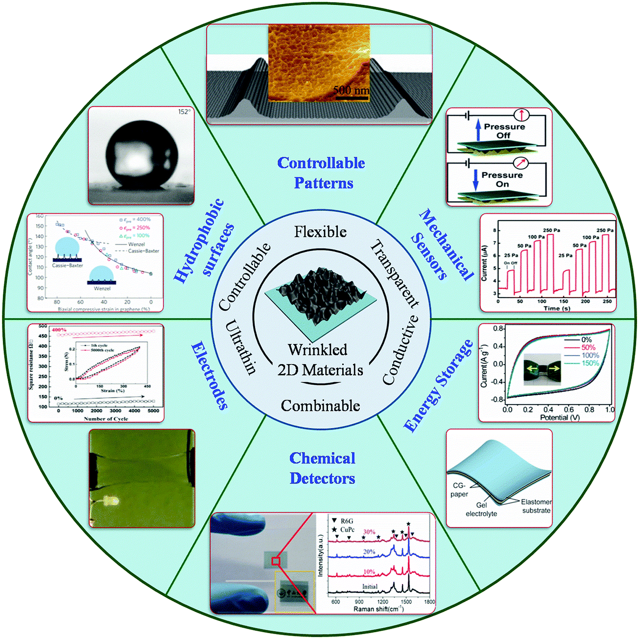 | ||
| Fig. 1 Overview diagram of wrinkled 2D materials demonstrating the features and applications. Figures of wrinkled 2D materials:58 Copyright 2017, Wiley-VCH Verlag GmbH & Co. KGaA, Weinheim. Figures of controllable patterns:60,61 Copyright 2014, Wiley-VCH Verlag GmbH & Co. KGaA, Weinheim. Copyright 2013, American Chemical Society. Figure of mechanical sensors:62 Copyright 2014, Wiley-VCH Verlag GmbH & Co. KGaA, Weinheim. Figures of hydrophobic surfaces:49 Copyright 2013, Macmillan Publishers Limited. Electrodes figure:63 Copyright 2016, Wiley-VCH Verlag GmbH & Co. KGaA, Weinheim. Figure of energy storage:64 Copyright 2014, Macmillan Publishers Limited. Figures of chemical detection:58 Copyright 2017, Wiley-VCH Verlag GmbH & Co. KGaA, Weinheim. | ||
2. Formation of wrinkles in 2D materials
In this section, based on the preparation methods and transfer processes of 2D materials, the approaches on controllable wrinkling in 2D materials will be discussed in detail. We also focus on the morphology and formation mechanism of these wrinkled structures. Eventually, some achievements in fabrication of wrinkles in 2D materials via various processes are summarized, as shown in Table 1.| Processes | Materials/substrates | Height, width, the aspect ratio or other characteristics | Controllability | Ref. | |
|---|---|---|---|---|---|
| Fabrication | Mechanical exfoliation | Graphene | ∼3 nm in height, ∼10 nm in width | Uncontrollable | 78 |
| MoS2 | ∼200 and ∼600 nm in height on SiO2 and Si3N4 substrates respectively | Uncontrollable | 42 | ||
| Talc | ∼2 nm in height | Uncontrollable | 73 | ||
| CVD synthesis | Graphene on Cu foils | Induced by grain boundaries, ∼4 nm in height | Uncontrollable | 98 | |
| Graphene on Cu foils | Induced by rough morphology, 1–5 nm in height, 5–25 nm in width | Controllable | 100 | ||
| MoS2 on Au foils | Induced by different thermal expansion coefficients, >1 nm in height | Uncontrollable | 86 | ||
| Transfer | Graphene on SiO2 | Wedging transfer, 3.3 ± 0.4 nm in height, 6.8 ± 2.2 nm in height | Uncontrollable | 127 | |
| Graphene on SiO2/Si | Polymer-supported transfer, 10–40 nm in height | Uncontrollable | 123 | ||
| Suspended GO on TiO2 islands | ∼200 nm in height, 0.8–4.2 μm in wavelength | Controllable | 128 | ||
| Graphene on organic solutions | 10–200 nm in height, the aspect ratio ∼0.1 | Controllable | 47 | ||
| GO on microstructured substrate | From hundreds of nanometers to micrometers in height | Controllable | 62 and 161 | ||
| CdS on pre-stretched substrates | 0.5–1 μm in height, 1–3.5 μm in wavelength | Controllable | 171 | ||
| ReSe2 on pre-stretched substrates | ∼100 nm in height, ∼1 μm in wavelength | Controllable | 183 | ||
| Graphene on thermally induced shrinkable substrates | ∼1.8 μm in height, ∼1.1 μm in width via uniaxial shrinkage; 2.5–3.3 μm in height, 1.3–1.7 μm in width via biaxial shrinkage | Controllable | 190 | ||
2.1 During the fabrication processes of 2D materials
Whatever method is used to prepare 2D materials, wrinkled structures are spontaneously formed in the samples. But the formation mechanism is different. For the samples fabricated by micromechanical exfoliation, the random formation of steps and wrinkles is due to the inhomogeneous breakage of layered van der Waals forces. For the samples fabricated by chemical vapor deposition (CVD), the rough topography of the growth substrates and the thermal stress during the cooling process jointly induced the formation of wrinkles in 2D materials. Additionally, it should not be neglected that crumpled and hierarchical structures of 2D materials can be easily obtained and controlled by the universal preparation method of chemical intercalation and exfoliation.65 The following sections mainly focus on the formation of wrinkles in 2D materials, which are prepared by micromechanical exfoliation and CVD.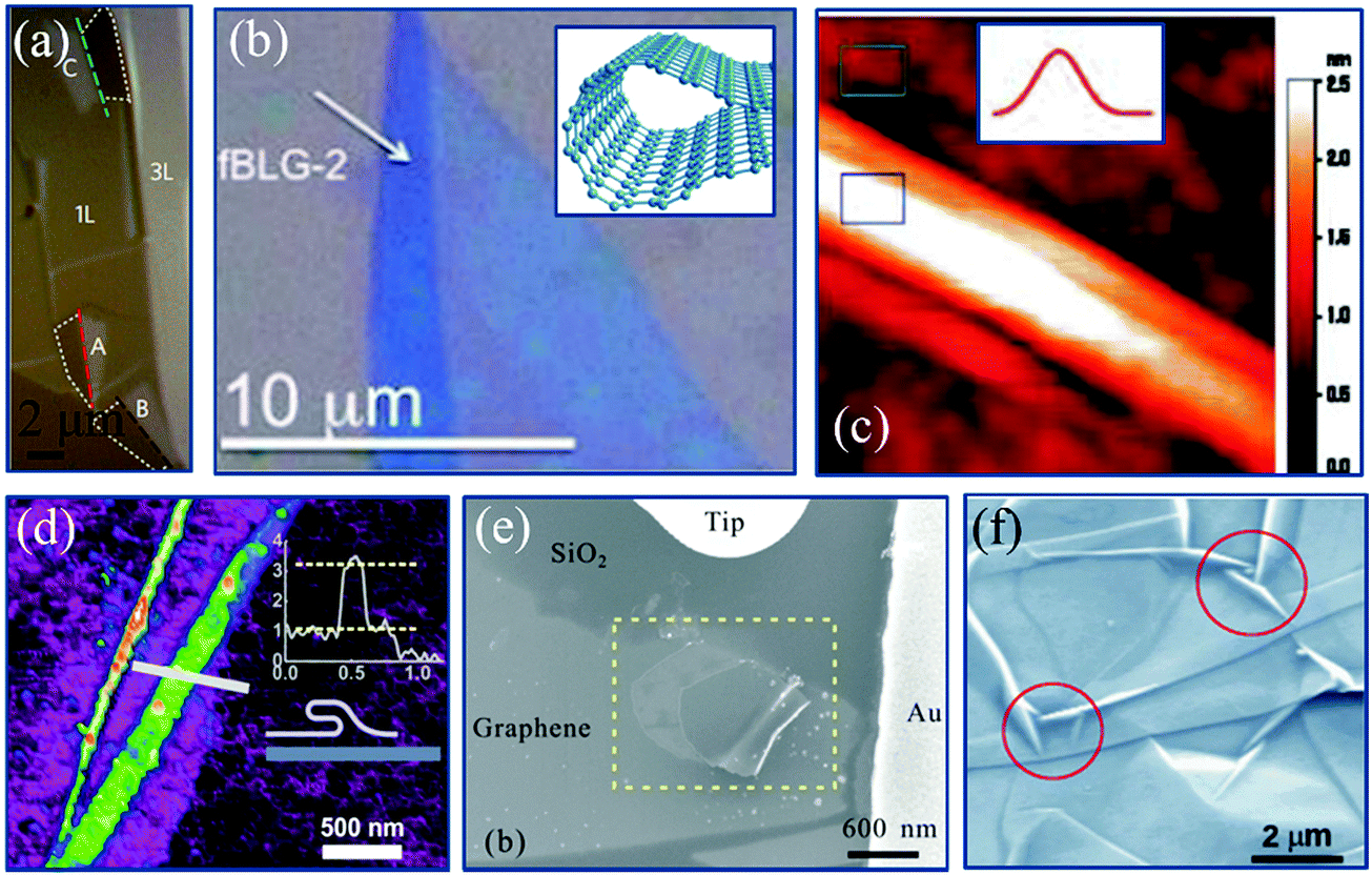 | ||
| Fig. 2 (a) Optical microscopy image of exfoliated MoS2.70 Copyright 2014, Macmillan Publishers Limited. (b) Optical microscopy image of scrolled graphene after exfoliation.76 Copyright 2012, American Chemical Society. Inset is the schematic of the graphene scroll.81 Copyright 2012, American Chemical Society. (c) Constant-current STM topograph of a graphene wrinkle.78 Copyright 2009, American Chemical Society. Inset is the schematic of the wrinkle.82 Copyright 2012, American Chemical Society. (d) AFM characterization of exfoliated 2D talc.73 Copyright 2015, IOP Publishing Ltd. (e) SEM image of curved graphene formed by mechanical manipulation.79 Copyright 2010, American Chemical Society. (f) Suspended exfoliated graphene.80 Copyright 2010, American Physical Society. | ||
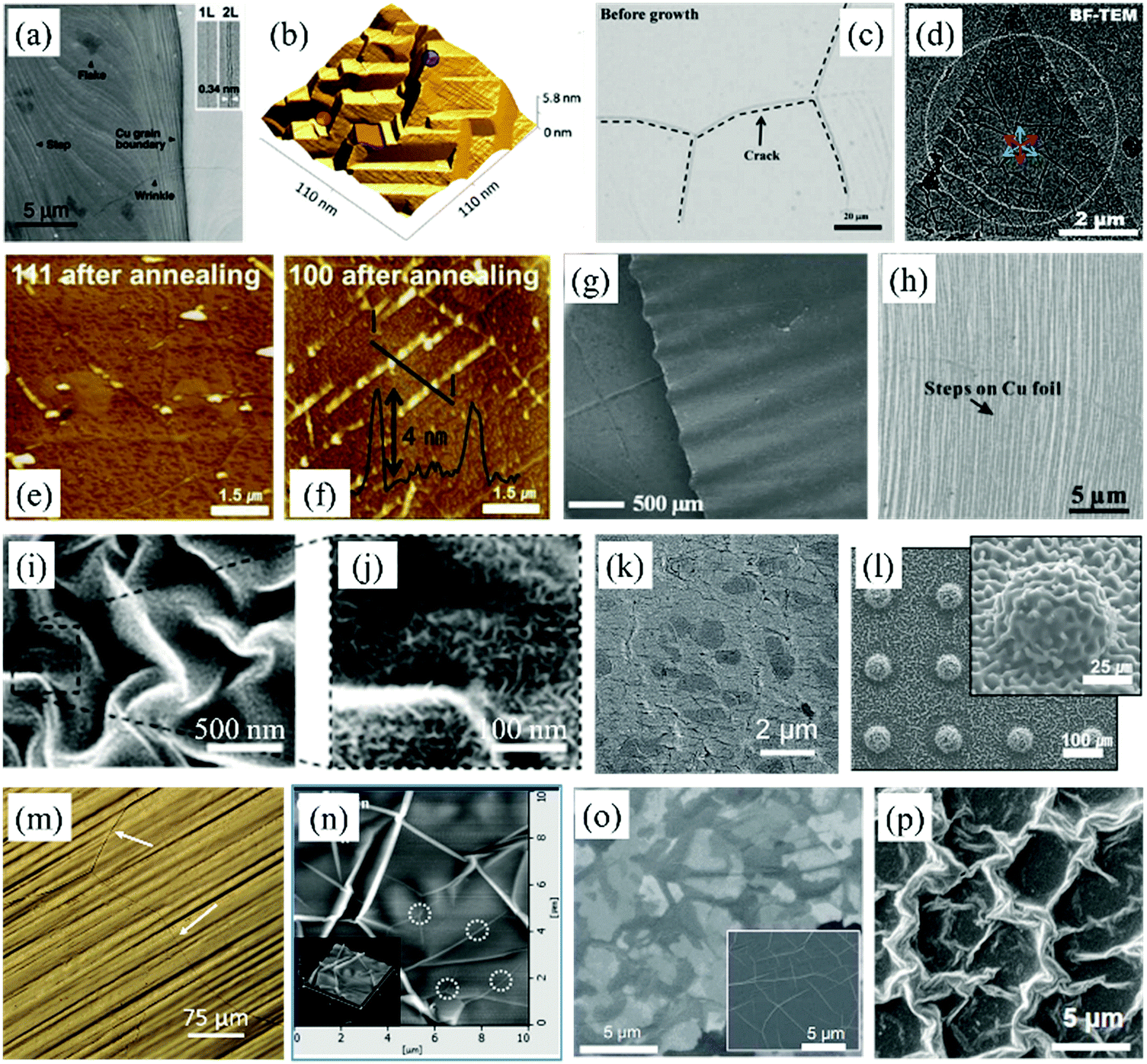 | ||
| Fig. 3 (a) SEM image of graphene on Cu foil.92 Copyright 2009, American Association for the Advancement of Science. (b) STM topography of a Cu substrate with steps.96 Copyright 2011, American Chemical Society. (c) Optical microscopy image of cracks on Ni foil after reduction.97 Copyright 2009, Wiley-VCH Verlag GmbH & Co. KGaA, Weinheim. (d) TEM image of MoS2.86 Copyright 2014, American Chemical Society. AFM image of graphene grown on (e) Cu(111) and (f) Cu(100) domain.98 Copyright 2013, The Royal Society of Chemistry. (g) SEM image of wrinkled graphene on a PDMS substrate.99 Copyright 2013, American Chemical Society. (h) SEM image of graphene grown on an orderly rough Cu substrate.100 Copyright 2011, American Chemical Society. (i) Low-magnification and (j) high-magnification image of crumpled MoS2 on a PS substrate.57 Copyright 2017, American Chemical Society. (k) SEM image of a graphene film grown on CNTs.102 Copyright 2016, Wiley-VCH Verlag GmbH & Co. KGaA, Weinheim. (l) SEM image of a hierarchically structured graphene array on PDMS.105 Copyright 2016, Wiley-VCH Verlag GmbH & Co. KGaA, Weinheim. (m) Optical microscopy image of graphene grown on Cu foil by CVD.47 Copyright 2016, American Chemical Society. (n) DFM image of graphene prepared on a Ni substrate.97 Copyright 2009, Wiley-VCH Verlag GmbH & Co. KGaA, Weinheim. (o) SEM images of graphene synthesized on thin and thick Ni foils (inset).113 Copyright 2009, Macmillan Publishers Limited. (p) SEM image of CVD-grown buckled MoS2 on a graphene substrate.114 Copyright 2016, American Chemical Society. | ||
Attempts have been made to construct parallel graphene wrinkles by synthesis of the samples on a Cu foil substrate with parallel wrinkle structures (Fig. 3g and h).99–101 Using this method, the distribution, namely, the distance between two wrinkles, can be tuned from hundreds of nanometers to hundreds of micrometers based on the target applications. Moreover, more and more patterns of wrinkles in 2D materials can be conveniently designed just by changing the surface topography of the growth substrates. Even MoS2 nanoflowers with the height of hundreds of nanometers have been prepared on a pre-processed patterned Au substrate (Fig. 3i and j).57 Last but not least, graphene films can also be directly grown on carbon nanotube (CNT) networks102–104 (Fig. 3k) and the metal substrate with hemisphere arrays (Fig. 3l)105 for further applications. Therefore, synthesizing 2D materials on patterned growth substrates is an effective way for the controlled fabrication of wrinkled structures. It is worth noting that standing graphene sheets can be grown directly in the vertical direction with the assistance of an air plasma by the method of plasma-enhanced CVD (Fig. 8f).106
Some other factors also could influence the formation of wrinkles in 2D materials during the CVD growth process. In the case of graphene, it is known that carbon atoms decompose from the carbon source (such as methane), dissolve in the melting metal foil at the high temperature and bond to form graphene during the cooling process.107 Commonly, there is a difference of thermal diffusivity between the metal substrate and the grown graphene, which could lead to the formation of additional wrinkles.97,108–110 It is indicated in Fig. 3m that the direction of graphene wrinkles introduced by thermal pressure on the Cu substrate is different from each other and easily identified, compared to the parallel wrinkles that follow the morphology of the growth substrate.47 Similar wrinkled structures can be distinguished in the graphene sample prepared on Ni substrates (Fig. 3n).97 Thermally induced wrinkles are also observable in other 2D materials synthesized on metal substrates by CVD, such as h-BN.111 The negative thermal expansion coefficient of graphene results in that its length increases during the cooling process, while the substrate has an opposite effect. This thermal compression forces the graphene wrinkling.32,112 What's more, in Fig. 3o, different thicknesses of the metal catalyst affect the dissolution of carbon atoms, then lead to the different topography of the as-synthesized graphene.113 Additionally, it is widely reported that 2D MoS2 films can be directly synthesized on Si substrates. Even buckled MoS2 structures (Fig. 3p) can be grown on graphene/Si substrates to form a hierarchical structure because the graphene layer imposes effects on the shape of MoS2 crumples.114,115 Besides, it is worth mentioning that random microstructures can be observed on graphene, its derivatives and TMDs prepared by other methods such as spray and chemical exfoliation.63,116–119
2.2 During the transfer processes of 2D materials
Irrespective of whether the 2D materials are peeled off from the bulk material by micromechanical exfoliation, synthesized by CVD or prepared by other methods, transferring them onto target substrates is a necessary procedure for further expected applications. During the transfer processes, the interactions between the 2D film and the substrate could affect the formation of new wrinkles. Furthermore, the wrinkled structures are also affected by the morphology or state of the target substrates.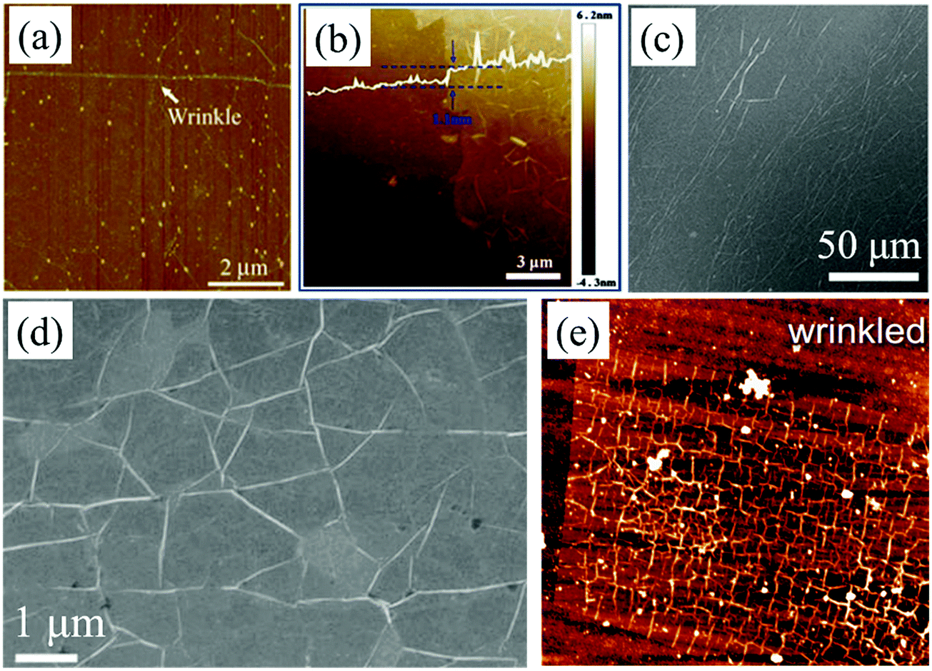 | ||
| Fig. 4 (a) AFM image of graphene transferred onto a SiO2/Si substrate.40 Copyright 2011, Tsinghua University Press and Springer-Verlag Berlin Heidelberg. (b) AFM characterization of graphene transferred onto a SiO2 substrate.87 Copyright 2013, Macmillan Publishers Limited. (c) SEM image of graphene on a polymer substrate based on the wet-transfer method.123 Copyright 2016, Wiley-VCH Verlag GmbH & Co. KGaA, Weinheim. (d) SEM image of graphene transferred onto a polycarbonate film.124 Copyright 2009, Elsevier Ltd. (e) AFM image of graphene after transfer.127 Copyright 2012, American Institute of Physics. | ||
If a 2D material is continuous and floats on aqueous solutions after etching the substrate, arbitrary target substrates, such as SiO2 (Fig. 4e), Si, quartz and polymers,47,58,60,113,125 can be used to intercalate into the liquid and “fish out” the sample onto it. This direct transfer process protects the sample from remaining impurities of the polymer support layer.47,58,60,113,125,126 During the water drain and drying procedures, the interfacial perturbation induces the formation of wrinkles with heights in the range of less than 20 nm, but which are not controllable.127 In contrast, a recent article has demonstrated that unidirectional and periodic wrinkles as high as 200 nm in graphene oxide can be acquired during its drying and solidification procedures with the assistance of a TiO2-gel-cracking process.128
The wedging transfer method is also applicable for the transfer of graphene onto the surface of other solutions, such as an ethanol/water solution with a certain concentration, to fabricate wrinkled graphene due to the interactions among the solid (graphene), liquid (ethanol solution) and air interfaces. The procedure is demonstrated in Fig. 5a.47 The height and distribution of the graphene wrinkles can be modulated just by modifying the concentration of the ethanol solutions. Essentially, the change of the surface tension at the interface is the key factor, based on which the formation of wrinkles can be controlled.129–133 It is found that the sudden decrease of the liquid surface tension from water (72.7 mN m−1) to ethanol solution (22.3 mN m−1 for pure ethanol) induces the self-organization of wrinkled graphene, based on Young's equation:47,134
γgs = γsl + γgl![[thin space (1/6-em)]](https://www.rsc.org/images/entities/char_2009.gif) cosθ cosθ |
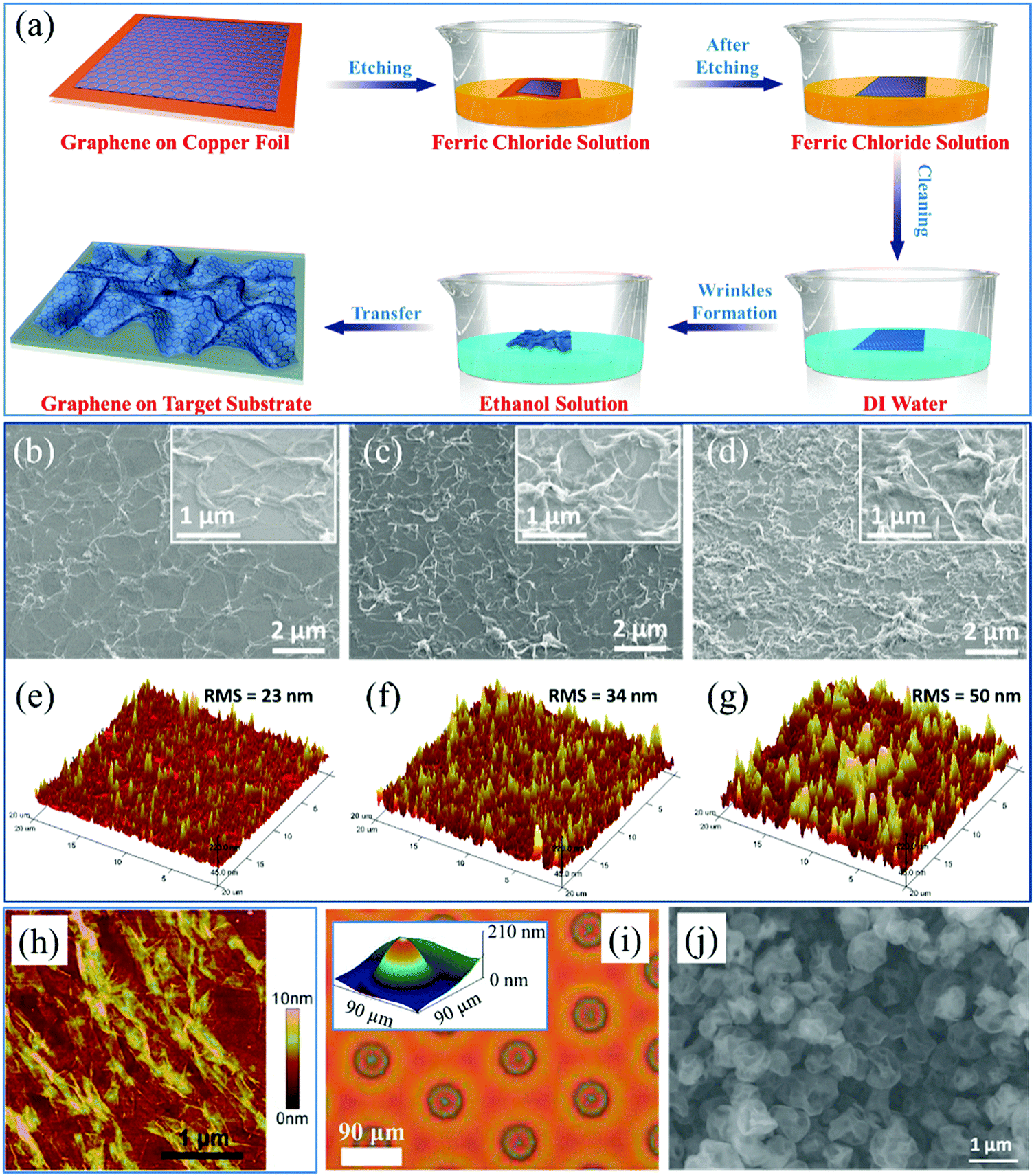 | ||
| Fig. 5 (a) Process schematics of fabrication of large-area wrinkled graphene on a solution surface.47 Copyright 2016, American Chemical Society. (b–d) SEM images of wrinkled graphene with different RMS assembled on the surface of ethanol/DI water solutions with different concentrations.47 Copyright 2016, American Chemical Society. (e), (f) and (g) 3D-view AFM images corresponding to (b), (c) and (d) respectively.47 Copyright 2016, American Chemical Society. (h) AFM image of wrinkled rGO after hydrazine vapor and thermal treatments.133 Copyright 2014, American Chemical Society. (i) AFM image of ordered protrusions on the surface of a polymer film. The inset is the 3D view.150 Copyright 2015, American Chemical Society. (j) SEM image of crumpled graphene nanosheets.121 Copyright 2015, Wiley-VCH Verlag GmbH & Co. KGaA, Weinheim. | ||
In our previous work, we indicated that Rayleigh–Bénard convection is another factor for interfacial instability, which could result in the formation of wrinkles in 2D materials. It can be quantitatively characterized by calculating the Rayleigh number Ra:136
| ΔEbending = −ΔG + WB |
| ΔG = γgl′ − γgs′ − γsl′ |
Actually, the generation of Rayleigh–Bénard convection is limited to the condition that the height to width ratio of the solution is high enough. In contrast, the Marangoni effect just happens in the thin layer or on the surface layer of liquids owing to the lateral gradient of surface tension, including that induced by the liquid flow or evaporation.136,139–144 The interfacial instability results from the fact that liquids flow from the regions with lower surface tension to that with higher surface tension. On the one hand, the liquid mass transfers along the interface between two fluids with different surface tensions. Resembling the Rayleigh number, the Marangoni number Ma is employed to study the Marangoni effect and is expressed by:139,145,146
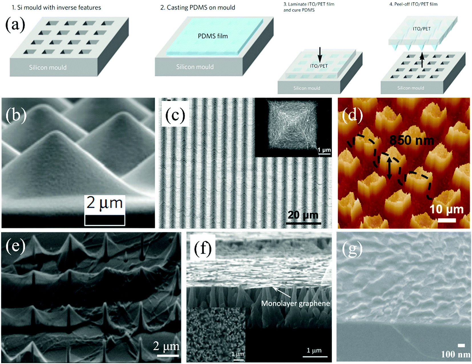 | ||
| Fig. 6 (a) Schematic of the procedure of the fabrication of a microstructured PDMS film.154 Copyright 2010, Macmillan Publishers Limited. (b) Tilted SEM image of micro pyramids on the as-fabricated PDMS film in (a) after peeling-off.154 Copyright 2010, Macmillan Publishers Limited. (c) SEM image of GO pyramids generated on the PDMS film. The inset is the high-magnification SEM image of a pyramid.62 Copyright 2014, Wiley-VCH Verlag GmbH & Co. KGaA, Weinheim. (d) 3D AFM view of GO arrays.161 Copyright 2016, Wiley-VCH Verlag GmbH & Co. KGaA, Weinheim. (e) SEM image of graphene transferred onto a Si substrate with pillar arrays.48 Copyright 2014, American Chemical Society. (f) SEM image of graphene on ZnO nanotips.166 Copyright 2012, American Institute of Physics. (g) SEM image of graphene on Si nanopillars.167 Copyright 2016, IOP Publishing Ltd. | ||
However, after the transfer onto the microstructured substrate, the 2D films do not always perfectly follow the morphology of the processed substrate and multiple wrinkled patterns can be shaped. For instance, as exhibited in Fig. 6e, a monolayer graphene film was transferred onto the Si substrate with pillar arrays by the support of a PMMA layer.48 After removing the PMMA layer, parts of the graphene were closely attached onto the Si pillars. And most of that are suspended between two corrugations with a certain distance. Graphene ripples with low height form on the flat areas of the Si substrate. The diversity of fabrication of graphene wrinkled patterns is mainly attributed to the distance between two neighboring pillars. A simple equilibrium condition is employed to interpret and is expressed by:48
| ΔE = Scξc − ErNr |
It is concluded that the formation of microstructures of 2D materials on patterned substrates dramatically relies on the morphology of the substrates. According to the simulated model mentioned above, the wrinkling of 2D films can be controlled by modifying the geometry of the target substrates.
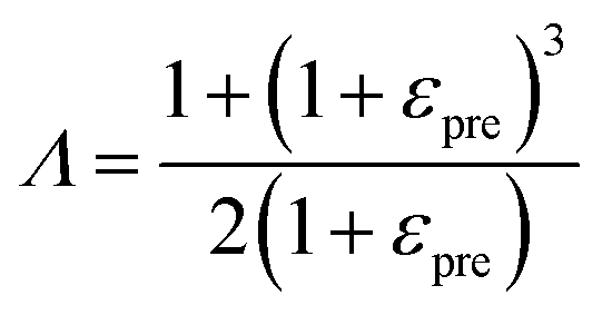
where h, E and v are the thickness, Young's modulus and Poisson's ratio of the 2D materials respectively, μ is the shear modulus of the elastomer substrate, and Λ is a parameter related to the pre-strain εpre expressed by:
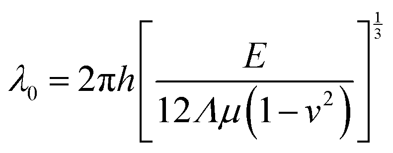
Accordingly, the features of the delaminated wrinkles are not only dependent on the intrinsic properties of the 2D materials and the stretchable substrate, but also strongly rely on the pre-strain of the substrate. During the relaxation process, compressive strain affects the fabrication of graphene wrinkles. If the tensile direction of the as-prepared wrinkled graphene on the polymer substrate is consistent with the shrinkage direction, the characteristics of the wrinkles at the present stage rely on the tension strain ε. Graphene restores its flat state when the tension reaches the pre-strain (ε = εpre) and cracks will emerge with continuously increasing strain (ε > εpre). In other words, the maximum stretchability of the wrinkled graphene is the pre-strain level of the elastomer substrate. However, the improvement of stretchability is unidirectional, that is, the stretchability of wrinkled graphene in the direction along the wrinkles is still in accordance with that of its flat counterparts. Stretching the wrinkled graphene in this direction still induces structural fractures, even though the applied tensile strain is much lower than the pre-strain level (ε < εpre).171 What's more, the flexible substrates can be stretched up to 400% in both directions (right inset of Fig. 7b), which results in the formation of 2D patterned wrinkles during the restoration of the elastic substrate, as shown in Fig. 7b.49 Equivalently, isotropic wrinkles are fabricated by the combination of two mutually perpendicular mechanical waves. The wave function of the wrinkled patterns is described as:179
where A is the maximum height of the wrinkles, λx and λy are the wavelength in two directions respectively. In the case of equally biaxial pre-strain, λx = λy, which enables the wrinkled graphene to be stretched in any directions without physical damage.

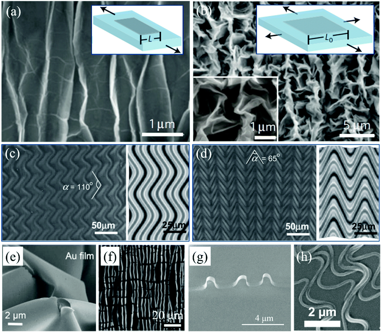 | ||
| Fig. 7 (a and b) SEM images of 1D and 2D graphene wrinkles on PDMS substrates respectively. Insets are the corresponding fabrication schematic diagrams.49 Copyright 2013, Macmillan Publishers Limited. (c and d) FEM simulations of wrinkles of polymer films formed by different strains and release sequences of the pre-stretched PDMS substrates.181 Copyright 2012, Wiley-VCH Verlag GmbH & Co. KGaA, Weinheim. (e) SEM image of wrinkled Au films under biaxial compression.182 Copyright 2016, American Chemical Society. (f) SEM image of CdS under uniaxial compression.171 Copyright 2016, Wiley-VCH Verlag GmbH & Co. KGaA, Weinheim. (g) SEM image of ReSe2 wrinkles.183 Copyright 2015, American Chemical Society. (h) SEM image of wave-like nanofibers.184 Copyright 2015, Wiley-VCH Verlag GmbH & Co. KGaA, Weinheim. | ||
Owing to this mechanical instability, it is reasonable to further devise different shrinkage sequences for the fabrication of various wrinkled patterns in 2D materials. There are two main factors to be controlled to tune the morphology. One is each pre-strain in two orthogonal directions jointly affecting the final wavelength of the wrinkles. The other is the direction-dependent relaxation order, which principally imposes its effects on the eventual direction of the wrinkles.180 The finite element method (FEM) gives simulated models to reveal the wrinkled patterns of an ethylene glycol diacrylate (EGDA) polymer thin film formed on the pre-stretched PDMS substrate after biaxial relaxation. In Fig. 7c, the larger strain (20%) is released first followed by the second relaxation of the smaller strain (10%) in the vertical direction leading to polymer wrinkles with a long wavelength and obtuse jog angles.181 In contrast, if the EDGA on PDMS with smaller pre-strain (20%) is first relaxed to its initial state followed by the release of the larger one, the obtained wrinkles possess shorter wavelength and much smaller jog angles (Fig. 7d).181 Therefore, it can be summarized that the pre-strains and release sequences in two stretching directions play synergistic roles in wrinkling of 2D materials. It is expected that much more wrinkled patterns will be acquired on the biaxially pre-stretched substrates by simultaneous and alternating multiple relaxations in two orthogonal directions. Because of the strong dependence on the properties and pre-strain states of the stretchable substrates, the wrinkled patterns cannot be transferred onto other substrates.
In recent years, theoretical feasibility and experimental facility have motivated this strain-based mechanical method to be applied for wrinkle construction in categories of 2D materials such as metal membranes (Fig. 7e),182 TMDs (Fig. 7f and g),171,183 and even 1D nanofibers (Fig. 7h).184 In addition, it is indicated that transferring a layer of thin film onto a stress-free polymer substrate followed by their repeated stretching would trigger the formation of buckled structures due to the mismatch of elastic properties such as Young's modulus and Poisson's ratio.185,186 By these methods, the corresponding physical properties of 2D materials can be effectively tuned, which significantly broaden their application fields.
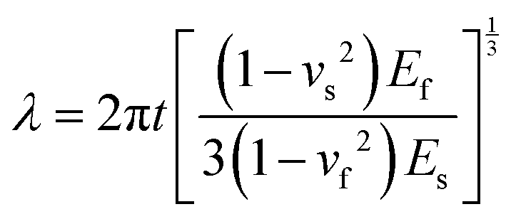
where t is the thickness of the thin film, vs and vf are the Poisson ratio of the substrate and film respectively, Es and Ef are Young's modulus of the substrate and film respectively. This mathematical model is also appropriate for other cases of wrinkle formation on hierarchical 2D materials. Accordingly, the 3D topography transformed from in-plane 2D morphology can be conveniently controlled by changing the thickness of the 2D film and the categories of the polymer substrate. 2D materials can be commonly prepared by highly controllable methods such as CVD, EB evaporation, sputter and spray techniques by which the thickness can be tuned. And different polymers possess different physical parameters such as Young's modulus, Poisson's ratio and critical temperature for mechanical deformation. It is noted that the wrinkling happens when the temperature reaches the critical one. The obtained wrinkled structures remain stable and do not release after cooling down to ambient temperature.
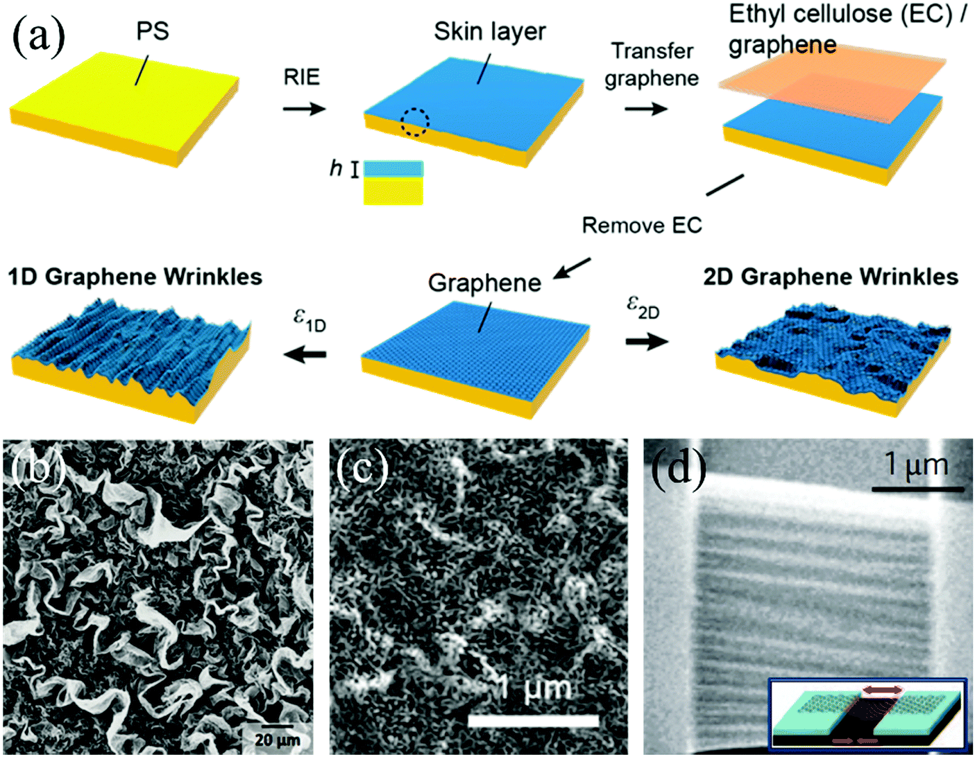
Regularly, these polymer substrates shrink biaxially to form isotropic wrinkles. As shown in Fig. 8a, isotropically wrinkled structures of graphene transferred onto a thermo-shrinkable polystyrene (PS) sheet are generated when the polymer substrate is heated above its glass transition temperature.50 1D wrinkles with a certain wavelength can be fabricated by fixing two sides of the composite sheet before the temperature rises to the critical value, which makes it retract uniaxially. Other than the natural properties of the retractable polymer substrates and 2D films, their multiple shrinkages also make important contributions to modulate the final patterns. For instance, Fig. 8b demonstrates the wrinkled topography of graphene formed by three-time shrinkage procedures, which complies with the 2D–1D–2D sequences.193 This method is also suitable for graphene composites to fabricate 3D structures (Fig. 8c).189 We conclude that controlling the shrinkage times and each corresponding direction is reasonable to manufacture much more 3D patterned surfaces in 2D materials,50,194 the height of which increases to three orders of magnitude compared with their original flat state (from several nanometers to micrometers).
 | ||
| Fig. 8 (a) Schematic of the process of fabrication of wrinkled structures on thermally induced shrinkable substrates.50 Copyright 2016, American Chemical Society. (b) SEM images of graphene crumples.193 Copyright 2016, Wiley-VCH Verlag GmbH & Co. KGaA, Weinheim. (c) SEM images of wrinkled graphene/gold nanoparticle composites.189 Copyright 2015, American Chemical Society. (d) SEM image of suspended graphene after thermal annealing.179 Copyright 2009, Macmillan Publishers Limited. | ||
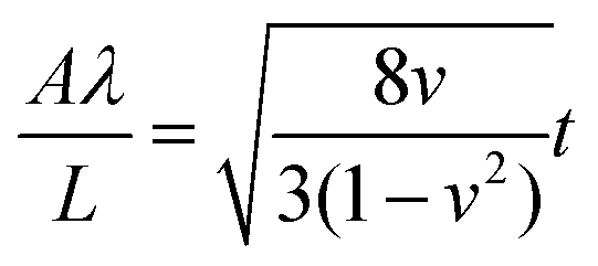
The other method for constructing thermo-induced wrinkles is not dependent on the mechanical properties but the negative thermal expansion coefficient of monolayer graphene. As illustrated in the inset of Fig. 8d, two sides of graphene are fixed, but not exactly on a substrate, and the rest suspends. With increasing temperature, uniform 1D graphene wrinkles form (Fig. 7d) under the uniaxial thermal pressure.179 The properties of the periodically suspended wrinkles are correlated with the nature of the initial thin film, which is elucidated by an equation:179,195
3. Properties
In the case of 2D materials, the structures play a very important role in their physical features including optical, mechanical, electrical and thermal properties. Different methods have been implemented to controllably fabricate 2D materials with a wrinkled structure to tune corresponding properties. The effects of mechanical, electrical and thermal properties of 2D materials imposed by the wrinkles are discussed in detail in the following sections.3.1 Mechanical properties
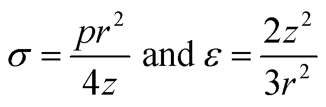
The mechanical properties of 2D materials, including stiffness, Young's modulus, breaking strength, Poisson's ratio, shearing and stretchability, are important for their realistic applications. These intrinsic properties are firstly affected by the lattice structures as well as the layer numbers. However, wrinkled patterns distort the perfect crystal structures and impose significant effects on the mechanical properties. Moreover, the wrinkled architecture can be controlled to tune the anisotropy of some properties. In addition, the mechanical nature can be conveniently modulated if the 2D materials are under deformation, specifically pressure and tension strain.where v is the Poisson ratio of graphene and taken as a constant, σ and ε are the stress and strain of graphene respectively; both are related to the applied pressure p, the vertical deflection at the center point z and the radius of the holes in the substrate r. Accordingly, σ and ε are simply given by:205
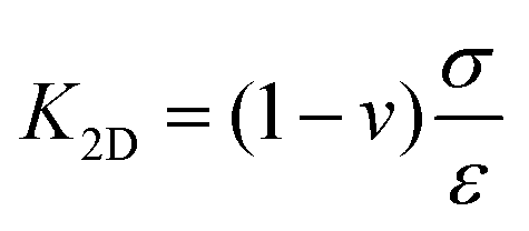
Then the in-plane Young's modulus E2D can be calculated by
Therefore, on account of the measurements of p and z, two featured mechanical properties can be calculated. Based on the nanoindentation method, it is obtained that the intrinsic Young's modulus and stiffness of flat graphene are ∼340 N m−1
 3,205 and ∼1 TPa,3,206 respectively. However, out-of-plane wrinkling induces dramatic changes in the mechanical characteristics of graphene, 2D materials beyond graphene and graphene based heterostructures, which can be tuned to improve their application potential.207 Commonly, Young's modulus and stiffness of flat 2D materials are constant and remain stable with increasing tensile strain. Namely, the σ–ε curve shows a linear correlation, as exhibited in Fig. 9c.205 But for wrinkled graphene, the non-linear elasticity (Fig. 9d) clarifies the changeable Young's modulus and stiffness during the tensioning process, because of the flattening of graphene wrinkles.205 Thus, the calculation of E2D needs to be modified to the differential form:
What's more important, the microstructures even trigger a one-order magnitude decrease of the graphene stiffness from the expected value of ∼340 N m−1 to a minimum of 20 N m−1.205 These studies offer a facile stretch-induced method to enhance the stiffness of 2D materials with wrinkled structures.61
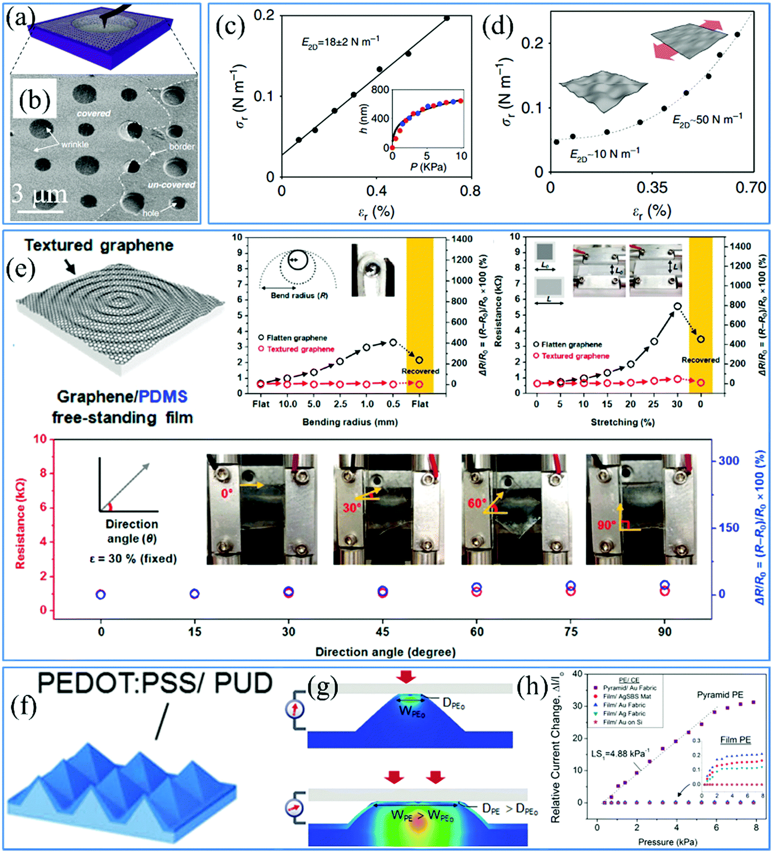 | ||
| Fig. 9 (a) Schematic illustration and (b) corresponding SEM image of graphene over a hole for nanoindentation measurements.4 Copyright 2013, American Association for the Advancement of Science. Stress–strain curve of (c) flat and (d) wrinkled graphene. The inset in (c) is the central deflection of graphene versus the applied pressure.205 Copyright 2015, Macmillan Publishers Limited. (e) Schematic of directionally uniform textured graphene and tests of its isotropic mechanical properties.209 Copyright 2016, American Chemical Society. (f) Schematics and (g) mechanism of a microstructured conductive PEDOT:PSS/PUD film and (h) its state and electrical measurements under compression.210 Copyright 2014, Wiley-VCH Verlag GmbH & Co. KGaA, Weinheim. | ||
Simultaneously, the breaking strength of graphene with the natural value of ∼42 N m−1 is significantly improved due to the existence of wrinkles.3,4 Here, another parameter related to the breaking strength, that is, stretchability is used to discuss the graphene features. Actually, there is an interplay between the stiffness and stretchability. In the study of the tensile deformation of conductive 2D materials, their electrical parameters such as resistance and current are widely employed to concretely reveal the structural modification. For instance, the resistance of graphene suddenly rises due to the emergence of fractures during the stretching process.208 It is reported in one of our previous works that a wrinkled architecture based on interfacial instability is able to enormously enhance the intrinsic stretchability of CVD-grown graphene of approximately 20% to over 100%.47 And its resistance changes slightly under a high tensile strain of 40%, which demonstrates the relaxation of graphene wrinkles without apparent physical degradation.47 Furthermore, wrinkled patterns impart anisotropic stretchability to 2D materials under elastic stretching, according to their directionality. As indicated in Fig. 9e, construction of omnidirectional graphene textures results in their isotropic stretchability, which is reflected by the unobservable changes of the resistance under the same tension strain of 30% in different stretching directions.209 For example, although 1D periodic graphene wrinkles determine the great improvement of stretchability in the direction across the wrinkle, along the wrinkle the original value is maintained.
In sum, the relevant elastic properties of 2D materials, such as Young's modulus, stiffness and stretchability, can be tuned by controlling the structure and morphology of the wrinkles in 2D materials. It cannot be ignored that wrinkles greatly promote the flexibility of 2D materials to withstand not only tensile strain, but also bending and torsion strain.47
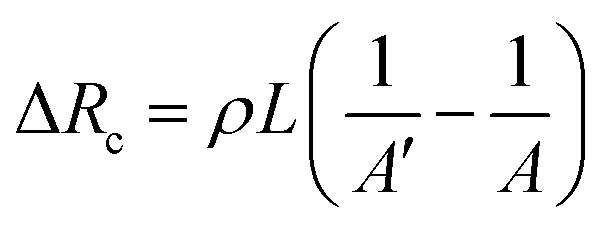
where ρ and L are the resistivity and length of the contact areas between two electrodes and both are taken as constant during the compression process, A′ and A are the contact area before and after compression. The collected electrical signals are mostly based on the change of contact areas, essentially current pathways in this case. As for 2D films with flat surfaces, applying pressures leads to slight changes in resistance owing to the changeless contact area. In contrast, two electrodes connect at the tip of the pyramids without pressure. When a small force is applied to the counter electrode, the lateral spread of the pyramids contributes to a dramatic increase in the contact area and more vertical conduction paths. Then the current responses increase with increasing applied force, as shown in Fig. 9h.210 Consequently, sharp wrinkled patterns deform easily under a smaller pressure in the elevation direction in comparison to the flat surfaces. These mechanical properties are widely used in the field of highly sensitive pressure sensors, which are reviewed in detail in Section 4.1.
3.2 Electrical properties
The lattice structures of 2D materials are expected to be exactly flat monolayers or perfectly layer-by-layer stacks. For instance, single-layer graphene has perfect in-plane hexagonal structures and its few-layer counterparts possess AB or ABC stacking lattices.211,212 As for TMDs and MXenes, multiple crystalline structures including 1T, 2H or/and α-phase have been found.213–216 Various electronic structures enrich their electrical properties and application fields. However, the lattice structures of these 2D materials are distorted by the inevitable wrinkles and external forces, which impose effects on the intrinsic electronic configuration, electron in-plane transport, band structure and so on. It is meaningful to mention that different levels of roughness of wrinkles produce contrasting electrical properties.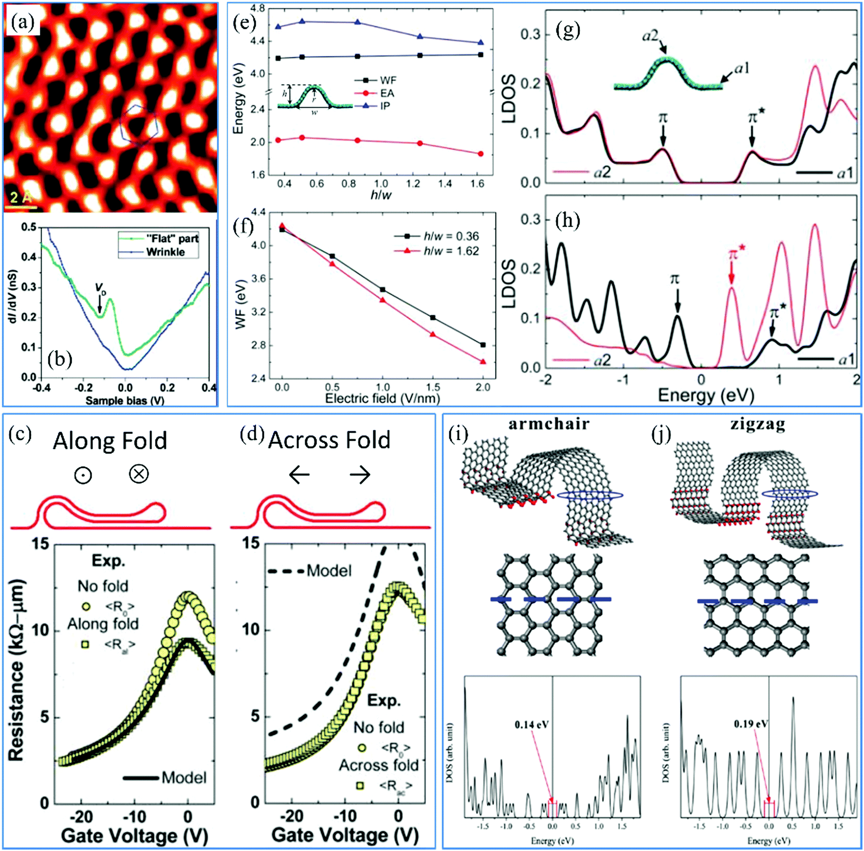 | ||
| Fig. 10 (a) Wrinkle-introduced distortion of lattice structures of graphene.78 Copyright 2009, American Chemical Society. (b) Conductance difference between the wrinkled and flat parts in the graphene film.78 Copyright 2009, American Chemical Society. Electrical conduction (c) along and (d) across the graphene fold.82 Copyright 2012, American Chemical Society. (e) Curves of work functions, electron affinities and ionization potentials versus height to width ratio respectively. Copyright 2012, American Chemical Society. (f) Work functions versus different height to width ratios. Copyright 2012, American Chemical Society. DOS of the wrinkled and flat areas of graphene (g) without and (h) with a bias voltage.224 Copyright 2012, American Chemical Society. Structural schematics and DOS along (i) armchair and (j) zigzag axes.45 Copyright 2013, American Chemical Society. | ||
Although graphene wrinkles negatively influence the mobility of carriers on the plane, it does not mean the degradation of the electrical conductance. Small ripples with a width of about 10 nm increase the resistance in both directions along and across the ripple due to the electron scattering.78 However, we have reported that the sheet resistance reduces with increasing surface roughness of graphene, which demonstrates wrinkle-introduced enhancement of conductivity. The topography of wrinkled graphene with high wrinkles is very similar to the few-layer stacking of graphene sheets (as in the schematics shown in Fig. 10c and d) and misorientations between the layers are present.82 Therefore, in the same areas of wrinkled graphene, external carriers transport multiple times and the graphene exhibits a much lower resistance (Fig. 10c) in the direction along the wrinkle, in comparison to that of flat graphene.82 The resistance across the graphene wrinkle is found to increase to a much higher extent due to the transported barrier built by the high wrinkle. However, extra current pathways are created that satisfy the motion of the current carriers between two stacking layers. The interlayer tunneling effect enhances the vertical conduction of electrons even if the height of wrinkles is up to hundreds of nanometers. Hence, it is profitable to keep the in-plane conductance of wrinkled graphene at the same level as that of its counterparts without folds (Fig. 10d).82 It is noted that if the length in one dimension of graphene is less than 5 nm, the conduction of the carriers in this direction will be confined.222 Consequently, the wrinkle-induced deformation of the intrinsic lattice structures does not degrade the electrical properties of 2D materials, but introduces many additional pathways for electron transfer.
It is supposed that there is no energy gap in the band structures of flat graphene, while semiconductive TMDs (MoS2, WS2, WSe2, MoSe2 and Mo2C) and insulated h-BN with a narrow band gap of 1–2 eV and a wide one of over 4 eV were frequently applied in devices.32 And the energy gaps can be tuned by modifying the lattice structures of the corresponding 2D crystals. Commonly, the present nanowrinkles with a height of less than 5 nm contribute to the deformation of crystalline structures under strain, which helps tune the forbidden gap of semiconductors, or even open the band gap of graphene with intrinsically metallic conduction.222 What's more, on the one hand, various energy gaps have been studied in different transport directions of external electrons (Fig. 10i and j).45 The band gap of graphene can be tuned in the small range of 0.14–0.19 eV, which is still much smaller than that of TMDs. On the other hand, graphene electrons at the location with higher curvature (small wrinkle width) possess lower energy. Then this triggers a wider band gap, which is comparable to that of TMDs.223 A recent study has found that wrinkle engineering of graphene is also a very significant way to change the band structure of molecules absorbed on its surface, according to the density functional theory simulation results.226 As for TMDs, such as WS2, wrinkles facilitate the modification of their bandgap and great enhancement of the intensity of photoluminescence.227 Actually, mechanical deformation such as tensile strain changes the bandgap as well as the optoelectronic properties of 2D materials.228–230
3.3 Thermal properties
In the case of high-quality monolayer graphene, the thermal diffusivity is found to be higher than that of any other 2D materials at ambient temperature. However, structural defects and wrinkles play active roles in thermal diffusion that the diffusivity is decreased to a lower level than the intrinsic value. Being similar to the measurement method of mechanical parameters, graphene needs to be transferred onto porous substrates in order to avoid the effects imposed by the thermal conductance at the graphene/substrate interface. But the difference is that the measured sample cannot be touched by any objects. Therefore, lasers are commonly used as the thermal source for heating the graphene. The schematic of the measurement device is illustrated in Fig. 11a and the Au-coated SiNx substrate with ordered holes is covered by the graphene membrane as shown in Fig. 11b.231 Wrinkles pose barriers to the thermal flux, which obviously degrades the thermal diffusivity of graphene (Fig. 11c).232 And the thermal diffusivity decreases with increasing surface roughness, as indicated in Fig. 11d.46 What's more, in graphene with 1D wrinkles, thermal conduction exhibits anisotropic behavior so that there is less heat flux transport across the wrinkles than that in the direction along the wrinkles. The schematics in Fig. 11e exhibit the directionality of the thermal flux. Fig. 11f further demonstrates that a much rougher morphology does not affect the thermal conductance along the wrinkles.46 But the thermal conductance in the flow direction across the wrinkles drops down synchronously. Accordingly, it is reasonable to interpret that the conductance of heat flux is dependent on the electron transport and collisions. And the electrons are collided by flexural phonons that block the thermal diffusion. Consequently, it is feasible to tune the wrinkling direction and level to control the reduction of thermal diffusion.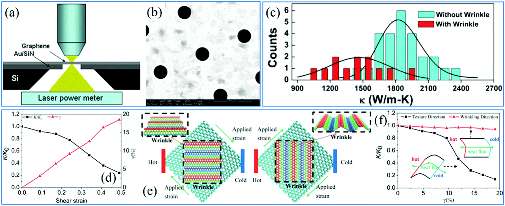 | ||
| Fig. 11 (a) Schematic illustration of a thermal measurement device and (b) SEM image of suspended graphene on an Au-coated SiNx substrate with ordered holes.231 Copyright 2010, American Chemical Society. (c) Thermal conductivity measurements of graphene with and without wrinkles. The solid curves are the Gaussian fitting of the corresponding histogram.232 Copyright 2012, IOP Publishing Ltd. (d) Relative thermal conductivity and wrinkling level versus shear strain.46 Copyright 2014, The Royal Society of Chemistry. (e) Schematics and (f) measurements of relative thermal conductivity along and across the graphene wrinkle.46 Copyright 2014, The Royal Society of Chemistry. | ||
4. Applications
Wrinkling offers a platform for 2D materials to broaden their applications in many fields. Firstly, the tunable mechanical strength enables the 2D film as the base materials to be applied in flexible electronics, which is a promising field. Particularly, the great improvement of flexibility, including stretchability, bending, torsion and compression strain, facilitates the 2D components to be integrated into flexible devices. By modifying the wrinkled patterns, it is possible to tune the relevant electrical properties and control the performance of 2D material based electronic devices. In addition, physical surface modification of 2D materials can be dependent on the construction of various wrinkled patterns. Therefore, in comparison to the flat 2D crystals, their wrinkled counterparts satisfy more realistic applications and meet the requirements for the good performance of 2D material based devices.4.1 Sensors
Several kinds of sensors based on 2D materials with ultralow thickness have become essential components integrated into electronic devices, which are widely applied in some cutting-edge fields such as artificial intelligence. Theoretically and experimentally, the wrinkled structures broaden the applications of flexible electronics because of the wrinkle-induced mechanical strength. For mechanical sensors and photodetectors, the mechanical deformation and incident lasers are collected and transformed into electrical signals for easy processing. The performance of these sensors, including the sensitivity, enhancement factor and stability, can be tuned by topographic engineering of the fundamental 2D materials. The multifunctionality of the flexible sensors is of great importance in practical detection.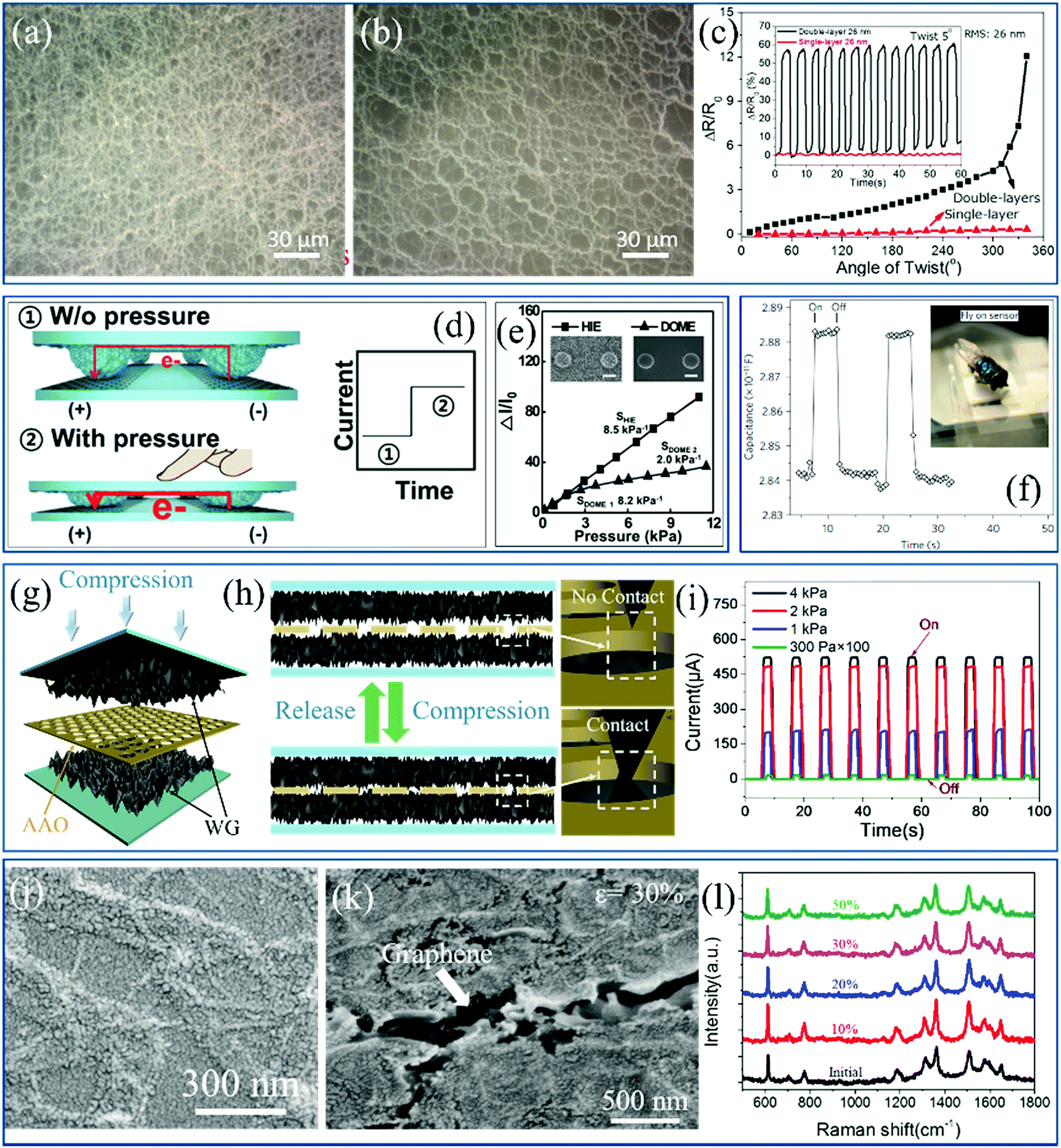 | ||
| Fig. 12 SEM image of (a) stack of double-layer and (b) single-layer wrinkled graphene and (c) detections of torsion strain by the sensors.47 Copyright 2016, American Chemical Society. (d) Mechanism schematic and (e) current changes versus the applied compressions of the traditional piezoresistive pressure sensor.105 Copyright 2016, Wiley-VCH Verlag GmbH & Co. KGaA, Weinheim. (f) Capacitance responses of a capacitive pressure sensor when detecting a fly.154 Copyright 2010, Macmillan Publishers Limited. Schematics of (g) structural engineering and (h) operating mechanism of a novel pressure sensor and (i) the current responses under differently applied compressions.126 Copyright 2017, American Chemical Society. SEM image of a wrinkled graphene/Au NPs hybrid SERS platform under (j) 0 and (k) 30% tensile strain and (l) the Raman spectra for detecting 10−6 M R6G solutions under various tensions.58 Copyright 2017, Wiley-VCH Verlag GmbH & Co. KGaA, Weinheim. | ||
Pressure sensor is another kind of mechanical device expected to be applied in flexible touch screens and robots for responding to the environmental tactile actions.62,105,129,155,160,239–241 The operating mechanism of these devices resembles the human skin in that the collected mechanical deformation is transformed into electrical signals including the changes in resistance and capacitance. The current and resistance responses generated in piezoresistive sensors are normally attributed to the change of contact areas, namely current pathways between two electrodes, as shown in Fig. 12d and e.105 Similarly, pressure induced by human touches or the gravity of objects (Fig. 12f) leads to the modification of the electrode distance in capacitance-based sensors for electrical responses.154 In both cases, wrinkled structures activate the sensors to enhance the sensitivity because a lower pressure is able to deform the wrinkles, in comparison to the 2D flat films.210 Furthermore, a new type of pressure sensor based on the combination of different 2D membranes has been reported by us. The structure is illustrated in Fig. 12g; a layer of porous and isolated anodic aluminum oxide (AAO) films is inserted between two wrinkled graphene electrodes.126 When a pressure is applied, wrinkles contact through the AAO pores to form current pathways, and are then separated after the removal of the force, as clarified in Fig. 12h.126 The simple mechanism avoids additional energy consumption at the off state of the combined sensors but also endows them with a high response sensitivity of 6.92 kPa−1 and high stability (Fig. 12i).126 This sandwich-like structure is expected to engage other 2D materials in compression detection. Subsequently, it is feasible to apply CNT membranes with a thickness of approximately 20 nm as electrodes and a photoresist blocking layer to fabricate resistive pressure sensors based on the same structure. The performance of sensors is improved to a much higher extent, including an ultrahigh sensitivity of 95.5 kPa−1, ultralow detection limit of 16 Pa and short response time of 16 ms.242 The sandwich-like model is also suitable for structural engineering of piezo-capacitive pressure sensors, which based on a layer of easily-accessible nylon netting sandwiched by two layers of graphene electrodes can even identify dynamic changes of a water droplet dropped onto the pressure sensor before being static.243 Accordingly, the operation performance of these mechanical sensors can be tuned by controlling the surface topography and scale of the used 2D materials.
Apart from the SERS platforms, other chemical sensors based on wrinkled 2D materials, such as graphene, graphene derivatives, and TMDs, are used to identify specific molecules.255–258 For instance, the absorption, even chemical bonding, of gas molecules on the detectors motivates the charge transfer and electrical responses, which are approved in the application of benchmarks or hygrometers. It has been reported that mechanical sensors based on low-dimensional carbon materials are able to detect the ambient temperature and humidity simultaneously, which fulfills the requirements of multifunctionality.259
4.2 Energy storage
Power sources such as new-type supercapacitors and batteries with small size, low thickness and mechanical strength are also needed for integration into flexible electronics. Based on the 2D materials with wrinkled structures as electrodes, the goals can be achieved. 2D films have high specific surface area and low height, which facilitates their combination with the electrochemical active materials to improve the performance. On the other hand, the supercapacitors are assured to operate stably under mechanical deformations because of the enhancement of flexibility induced by the wrinkles. In addition, the performance of the promising lithium and lithium–sulfur batteries is dramatically benefited from the high stretchability and specific surface area of wrinkled electrode materials.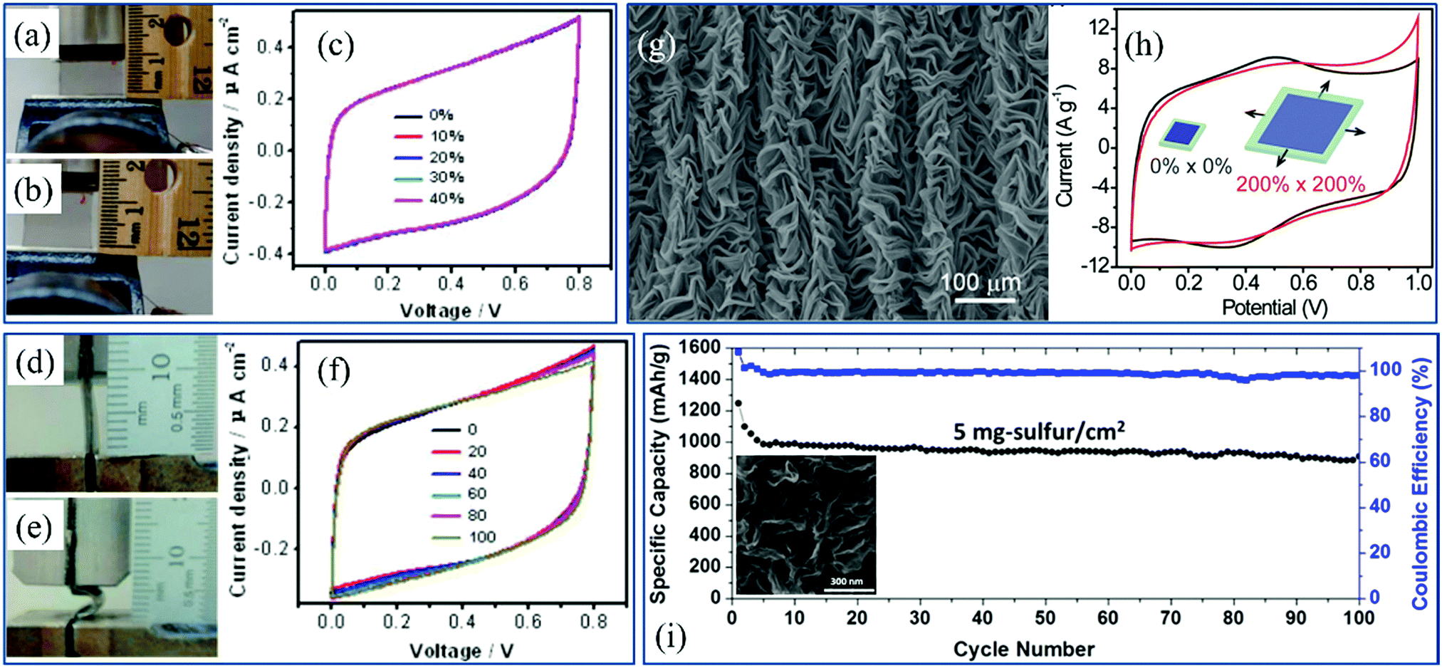 | ||
| Fig. 13 Photograph of the electrode of a supercapacitor based on wrinkled graphene (a) at the initial state and (b) under tensile strain and (c) the performance of the electrode under various tensions.99 Copyright 2013, American Chemical Society. Photograph of the electrode of a supercapacitor based on wrinkled graphene (d) at the initial state and (e) under bending strain and (f) the electrochemical performance of the electrode under various bending strains.99 Copyright 2013, American Chemical Society. (g) SEM image of wrinkled graphene and (h) the performance of wrinkled graphene based electrodes in energy storage under biaxial tensile strain.64 Copyright 2014, Macmillan Publishers Limited. (i) Cycling stability and Coulombic efficiency of the cathode of a lithium–sulfur battery based on crumpled graphene. The inset is the SEM image of crumpled graphene.272 Copyright 2015, American Chemical Society. | ||
In Li–S batteries, during the charge–discharge cycles, the production of lithium polysulfides lowers the utilization of sulfur and decreases the active materials. Thus, the existence of intermediates limits the performance and further applications of the batteries. As shown in the inset of Fig. 13i, wrinkled graphene sheets are used to coat the sulfur, the numerous nanopores offered by which enhance the specific surface area as well as the absorption of lithium polysulfides.272 And the graphene wrinkles serve as obstacles for polysulfide shuttle. Therefore, the cyclability can be improved to a much higher extent (Fig. 13i).272 With active holders and flexible supporters, batteries based on wrinkled 2D materials are promising to be applied in next-generation energy storage.
4.3 Field electron emission
The performance of field electron emission (FEE) cathodes relies not only on the materials but also on their surface morphology. High-curvature wrinkles change the band structure of 2D materials and decrease their electron affinities, which facilitates the emission of the external electrons in a vacuum and enhances the stability. Therefore, in combination with ultralow thickness, high transparency and outstanding performance, cathodes based on 2D materials and their composites are attractive emitters to be applied in FFE. Furthermore, in contrast to the traditional cathode material ITO without flexibility, the great improvement of stretchability induced by wrinkles approves the wide application of microstructured 2D materials in next-generation flexible panel displays.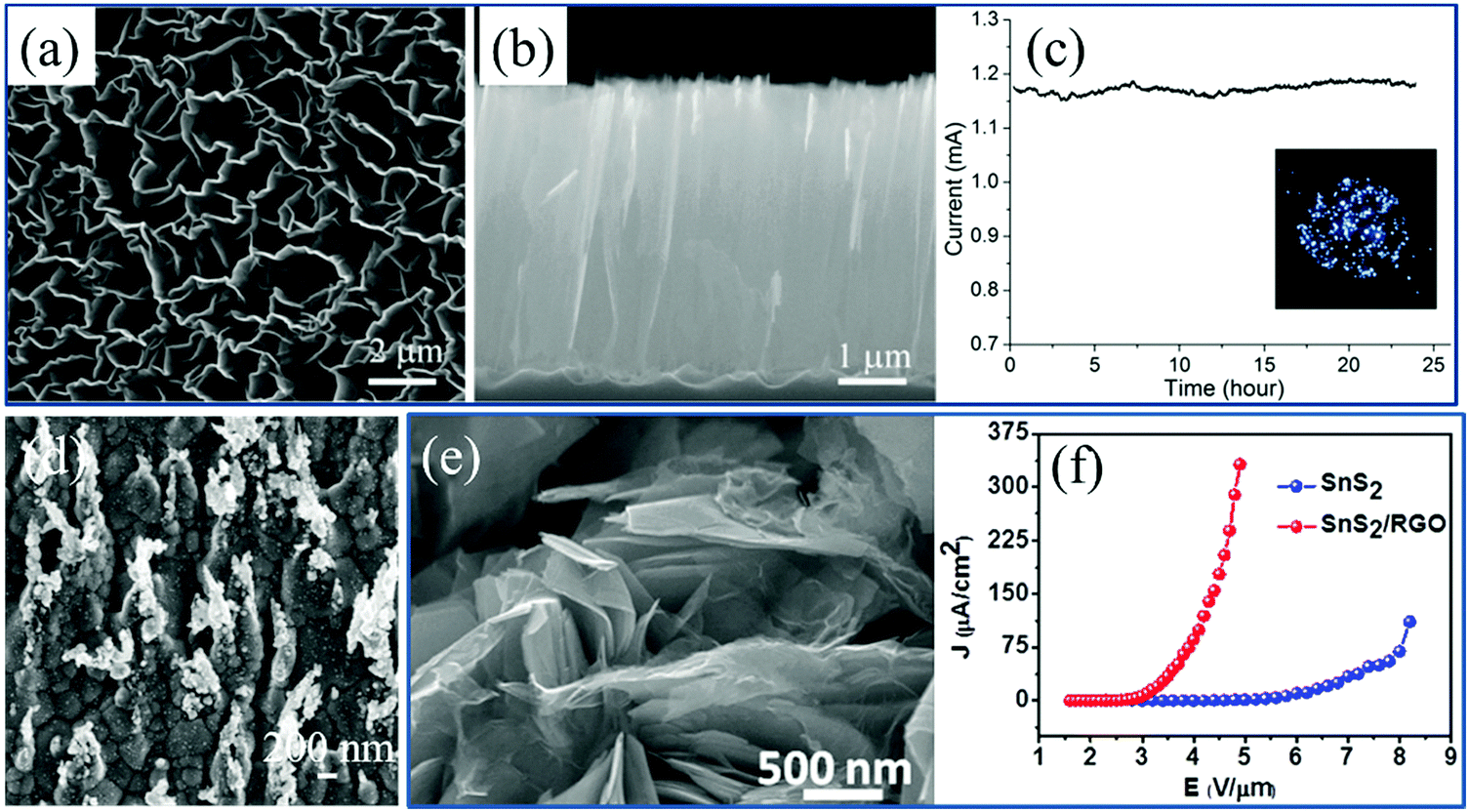 | ||
| Fig. 14 (a) Top-view, (b) side-view SEM image and (c) FEE performance of standing graphene sheets.106 Copyright 2012, IOP Publishing Ltd. (d) SEM image of MoS2 on silver nanotips.287 Copyright 2016, American Institute of Physics. (e) SEM image and (f) FEE performance of SnS2/RGO composites.281 Copyright 2014, American Institute of Physics. | ||
Enhancement factor (EF) β is a common criterion for characterizing the FFE performance of all these emitters. It can be easily calculated according to the Fowler–Nordheim equation and the slope k of the F–N plots corresponding to the current density to electric field curves:282–284
| β = −Bϕ3/2/k |
Consequently, the synergistic properties of high stretchability, low thickness, high transparency and great FEE characteristics enable the emission cathodes based on single and composite 2D materials with roughened morphology to be applied in flexible displays. The next generation of touch screens is expected to be integrated into wearable electronic devices and stably work under mechanical deformation.
4.4 Superhydrophobic surfaces
Construction of superhydrophobic surfaces on 2D materials is inspired by the surface structures of some natural plants such as lotus leaf. With the advantages of self-cleaning, anti-contamination and water immersion resistance, the improvement of hydrophobicity meets the requirement of the multifunctionality of the devices based on 2D materials. And they are found to operate normally under special and extreme circumstances. The flat layered 2D materials such as graphene and MoS2 show weak hydrophobicity, which is dependent on the layer numbers. However, the main factor for determining their wetting properties is the wrinkled structures on the surface.49 It is possible to engineer different microstructures with controllable height and distribution on the surface of 2D materials for modulating the hydrophobicity. As shown in Fig. 15a, the schematic illustrates a processed Au substrate with standing nanostructures, on which MoS2 can be directly synthesized by the method of CVD.57 After shrinkage due to the mechanical compression, the hydrophobicity of the nanoflower-like MoS2 surfaces can be greatly improved from 90° to the superhydrophobic level of more than 150° (Fig. 15b).57 What's more, the height of the MoS2 nanoflowers can be tuned in the nanoscale range, which is advantageous for the manipulation of their wetting properties. | ||
| Fig. 15 (a) Schematic illustration MoS2 nanoflowers and (b) AFM characterization (scale bar: 1 μm) and corresponding droplet images (scale bar: 500 μm) at different tensile strains.57 Copyright 2017, American Chemical Society. (c) Water contact angle of wrinkled graphene samples with different RMS on microstructured sapphire substrates. The inset is the SEM image of wrinkled graphene with a RMS of 35 nm on microstructured sapphire.51 Copyright 2017, Elsevier Ltd. | ||
Engineering rough structures improves the hydrophobicity of the surfaces as well as the flexibility of the formed 2D membrane. On the one hand, corrugated 2D MoS2 shows dynamically changeable surface properties (water contact angle) driven by being stretched because of the structural changes of wrinkles under tension strain.288 On the other hand, it is reasonable to think that the synergy of both properties is suitable for modifying the wetting properties of other flat or roughened surfaces. Actually, this physical modification technique is very simply applicable to transfer microstructured 2D thin films onto hydrophilic substrates. Considering the target substrates with ordered or irregular corrugations, the transferred 2D materials suffer from mechanical deformation but without structural degradation owing to the high stretchability. Furthermore, the corrugated substrates serve as a mold, over which the membrane follows the topography and makes the surfaces waterproof. For instance, the bare sapphire substrate with ordered micropyramids is superhydrophilic with a water contact angle of less than 10°. A layer of wrinkled graphene with a RMS of 35 nm can be directly transferred onto it to achieve a hydrophobic surface so that the contact angle increases up to more than 130° (Fig. 15c).51 Consequently, the structures on the surface play a more important role in the hydrophilicity and hydrophobicity rather than the layer number of the layered 2D materials.
4.5 Electrodes
Flexible electronics based on 2D materials also require the flexibility of electrical circuit integrated into them. The deposition of conductive materials such as metals, graphene and MoS2 on pre-stretched polymer substrates is a common method to prepare 2D films with crumpled structures. The flexibility of these wrinkled 2D materials is suitable for their applications in flexible devices such as sensors and transistors.63,152,169,183,289–292 The stable conductivity of the crumpled electrodes under mechanical deformation does not induce additional negative effects on the electronic devices. In the case of field effect transistors (FETs), the gate dielectric materials are the key factor to fabricate flexible devices.293 Therefore, in comparison to the flat 2D films, the gate dielectric with wrinkled structures fulfills the requirements of flexible FETs.5. Conclusions and outlook
This review has introduced the research progress in 2D materials with wrinkled structures. Random corrugations with low height form during the preparation and transfer processes. However, wrinkles can be controllably fabricated relying on the morphology of the growth or/and target substrates as well as the stress via releasing the pre-stretched target substrates. Furthermore, the self-assembly of homogeneous wrinkles with tunable height and distribution can be induced by the interactions at the liquid–gas interfaces, laser radiation and the compression induced by thermally shrinkable polymers. The mechanism of these methods and structural features of the as-prepared wrinkled structures have been discussed. The wrinkled structures generate significant changes of the physical properties of 2D materials, including the mechanical properties, electronic mobility, and energy band structures, etc. Thus, these directional properties can be tuned by controlling the wrinkling and modified dynamically by stretching the 2D materials. Consequently, with the introduction of many outstanding properties, wrinkles in 2D materials optimize their promising applications in field emission, surface modification, sensors and field effect transistors. However, some major challenges still need to be addressed for universal applications of patterned 2D materials.One of the main challenges is the development of the controllability of high-quality patterned 2D materials with expected properties. Several methods such as the transfer of 2D materials onto organized microstructured substrates, pre-stretched polymer substrates and organic solutions are highly controllable for fabrication of periodically 1D, uniformly 2D or variously patterned wrinkles. The height of these wrinkled structures can be modified as well. However, a method is still needed to control a single wrinkle with expected height and direction at a certain location, which is very advantageous to pave a way for manufacturing electronic devices and studying the relevant properties. In addition, the fabrication of wrinkled patterns reported previously relies on the mechanical deformation of the polymers, onto which the microstructured 2D materials are not able to be transferred subsequently. But some electronics, FETs for instance, require the employed 2D materials to be transferred onto Si or SiO2 substrates. Therefore, efforts should be made to find substrate-independent methods to improve the tunability of wrinkled structures in 2D materials. Cost is also a focus for common and commercial applications of wrinkled 2D material-based devices.
As the first important 2D material, the wrinkle-induced mechanical, electrical, thermal and optical properties of graphene have been comprehensively studied. Particularly, the distortion of the graphene lattice structures generated by the wrinkled structures degrades the in-plane mobility of electrons, increases the conductivity as well as opens the band gap. Thus, engineering wrinkles in TMDs or MXenes has the potential to be a facile, effective and reasonable method for the modification of their energy band structures and electrical properties. However, recent studies focusing on this field are rare. The electrical properties of wrinkled 2D materials beyond graphene should be further explored for their applications in electronic devices.
With atomic thickness and special electronic structures, different categories of 2D materials are desirable to be combined for applications. Recently, layered or lateral heterostructures based on flat 2D TMDs have been widely manufactured for electronic and optoelectronic devices. Accordingly, it is foreseen that studying the electronic behaviors of vertical and lateral homostructures, heterostructures and other junctions based on the stacking or contact of different wrinkled 2D films is a new research direction. Thus, the synergy of different 2D materials with wrinkles broadens their application fields to a much wider extent and drives the rapid development of next-generation electronic devices.
Wearable electronics is a hot topic where microstructured 2D crystals are employed as the basic materials. Wrinkles significantly improve the flexibility of the 2D materials and ensure their stable operation under mechanical deformation. Ultralow height and weight also agree with the concept of “wearable”. In particular, flexible capacitive and piezoresistive sensors based on 2D materials with wrinkles have been widely applied in electronic skins, health monitors and touch apparatus. But in most of these cases, the electrodes, batteries and other needed devices are based on traditional materials without flexibility, which is disadvantageous for their integration and further practical applications. Although it is possible to fabricate flexible electrodes and electrical circuits on pre-stretched or thermally induced shrinkable substrates, the metal membranes easily come off the organic substrates owing to the weak adhesion. Therefore, the integration techniques should be further improved for the accomplishment of wearable electronics.
In summary, there are categories of 2D materials exhibiting metallic (such as graphene), semiconductive (such as TMDs) or insulating (such as h-BN and polymers) behaviors. And wrinkle engineering significantly modifies the energy band structure, thus tuning the mechanical and electrical properties of 2D materials and heterostructures based on these materials. The rapid development of studies on all classes of wrinkled 2D materials with tunable properties may bring a bright future for further potential applications. Therefore, different categories of wrinkled 2D materials with different properties are expected to be applied in corresponding fields. 2D materials with wrinkled patterns and excellent properties should be selected according to expected applications.
Conflicts of interest
There are no conflicts to declare.Acknowledgements
This work was financially supported by the National Natural Science Foundation of China (Grant No. 51772335), the Natural Science Foundation of Guangdong Province (Grant No. 2016A030313346 and 2014A030306022), and the Guangdong Youth Top-notch Talent Support Program (No. 2015TQ01C201).References
- K. S. Novoselov, A. K. Geim, S. V. Morozov, D. Jiang, Y. Zhang, S. V. Dubonos, I. V. Grigorieva and A. A. Firsov, Science, 2004, 306, 666–669 CrossRef CAS PubMed.
- A. K. Geim and K. S. Novoselov, Nat. Mater., 2007, 6, 183–191 CrossRef CAS PubMed.
- C. Lee, X. Wei, J. W. Kysar and J. Hone, Science, 2008, 321, 385–388 CrossRef CAS PubMed.
- G. H. Lee, R. C. Cooper, S. J. An, S. Lee, A. van der Zande, N. Petrone, A. G. Hammerberg, C. Lee, B. Crawford, W. Oliver, J. W. Kysar and J. Hone, Science, 2013, 340, 1073–1076 CrossRef CAS PubMed.
- F. Bonaccorso, Z. Sun, T. Hasan and A. C. Ferrari, Nat. Photonics, 2010, 4, 611–622 CrossRef CAS.
- A. A. Balandin, Nat. Mater., 2011, 10, 569–581 CrossRef CAS PubMed.
- D. Voiry, J. Yang, J. Kupferberg, R. Fullon, C. Lee, H. Y. Jeong, H. S. Shin and M. Chhowalla, Science, 2016, 353, 1413–1416 CrossRef CAS PubMed.
- D. Lin, Y. Liu, Z. Liang, H.-W. Lee, J. Sun, H. Wang, K. Yan, J. Xie and Y. Cui, Nat. Nanotechnol., 2016, 11, 626–632 CrossRef CAS PubMed.
- J.-J. Shao, W. Lv and Q.-H. Yang, Adv. Mater., 2014, 26, 5586–5612 CrossRef CAS PubMed.
- M. Pumera and Z. Sofer, Adv. Mater., 2017, 29, 1605299 CrossRef PubMed.
- H. Liu, Y. Du, Y. Deng and P. D. Ye, Chem. Soc. Rev., 2015, 44, 2732–2743 RSC.
- Z. Zhang, S. N. Shirodkar, Y. Yang and B. I. Yakobson, Angew. Chem., Int. Ed., 2017, 56, 15421–15426 CrossRef CAS PubMed.
- S. Sharma, S. Kumar and U. Schwingenschlogl, Phys. Rev. Appl., 2017, 8, 044013 CrossRef.
- J. Xu, S. Wang, G.-J. N. Wang, C. Zhu, S. Luo, L. Jin, X. Gu, S. Chen, V. R. Feig, J. W. F. To, S. Rondeau-Gagne, J. Park, B. C. Schroeder, C. Lu, J. Y. Oh, Y. Wang, Y.-H. Kim, H. Yan, R. Sinclair, D. Zhou, G. Xue, B. Murmann, C. Linder, W. Cai, J. B. H. Tok, J. W. Chung and Z. Bao, Science, 2017, 355, 59–64 CrossRef CAS PubMed.
- H. Shi, C. C. Liu, Q. L. Jiang and J. K. Xu, Adv. Electron. Mater., 2015, 1, 1500017 CrossRef.
- G. F. Cai, P. Darmawan, M. Q. Cui, J. X. Wang, J. W. Chen, S. Magdassi and P. S. Lee, Adv. Energy Mater., 2016, 6, 1501882 CrossRef.
- P. Eklund, J. Rosen and P. O. A. Persson, J. Phys. D: Appl. Phys., 2017, 50, 113001 CrossRef.
- N. K. Chaudhari, H. Jin, B. Kim, D. S. Baek, S. H. Joo and K. Lee, J. Mater. Chem. A, 2017, 5, 24564–24579 RSC.
- Y. Yoon, K. Lee and H. Lee, Nanotechnology, 2016, 27, 172001 CrossRef PubMed.
- C. Xu, L. Wang, Z. Liu, L. Chen, J. Guo, N. Kang, X. L. Ma, H. M. Cheng and W. Ren, Nat. Mater., 2015, 14, 1135–1141 CrossRef CAS PubMed.
- G. Cassabois, P. Valvin and B. Gil, Nat. Photonics, 2016, 10, 262–266 CrossRef CAS.
- Q. Weng, X. Wang, X. Wang, Y. Bando and D. Golberg, Chem. Soc. Rev., 2016, 45, 3989–4012 RSC.
- D. Voiry, A. Mohite and M. Chhowalla, Chem. Soc. Rev., 2015, 44, 2702–2712 RSC.
- Y. J. Zhang, M. Yoshida, R. Suzuki and Y. Iwasa, 2D Mater., 2015, 2, 044004 CrossRef.
- P. K. Kannan, D. J. Late, H. Morgan and C. S. Rout, Nanoscale, 2015, 7, 13293–13312 RSC.
- M. Onga, Y. Zhang, T. Ideue and Y. Iwasa, Nat. Mater., 2017, 16, 1193–1197 CrossRef CAS PubMed.
- Z. Zhang, J. Niu, P. Yang, Y. Gong, Q. Ji, J. Shi, Q. Fang, S. Jiang, H. Li, X. Zhou, L. Gu, X. Wu and Y. Zhang, Adv. Mater., 2017, 29, 1702359 CrossRef PubMed.
- K. Kalantar-zadeh, J. Z. Ou, T. Daeneke, A. Mitchell, T. Sasaki and M. S. Fuhrer, Appl. Mater. Today, 2016, 5, 73–89 CrossRef.
- J. Mei, T. Liao, L. Kou and Z. Sun, Adv. Mater., 2017, 29, 1700176 CrossRef PubMed.
- M. Zhao, Q. Zhao, B. Li, H. Xue, H. Pang and C. Chen, Nanoscale, 2017, 9, 15206–15225 RSC.
- H. Yin and Z. Tang, Chem. Soc. Rev., 2016, 45, 4873–4891 RSC.
- X. Li, L. Tao, Z. Chen, H. Fang, X. Li, X. Wang, J.-B. Xu and H. Zhu, Appl. Phys. Rev., 2017, 4, 021306 Search PubMed.
- G. Fiori, F. Bonaccorso, G. Iannaccone, T. Palacios, D. Neumaier, A. Seabaugh, S. K. Banerjee and L. Colombo, Nat. Nanotechnol., 2014, 9, 768–779 CrossRef CAS PubMed.
- Y. Saito, T. Nojima and Y. Iwasa, Supercond. Sci. Technol., 2016, 29, 093001 CrossRef.
- D. Jariwala, T. J. Marks and M. C. Hersam, Nat. Mater., 2017, 16, 170–181 CrossRef CAS PubMed.
- K. S. Novoselov, A. Mishchenko, A. Carvalho and A. H. C. Neto, Science, 2016, 353, aac9439 CrossRef CAS PubMed.
- Y. Liu, N. O. Weiss, X. D. Duan, H. C. Cheng, Y. Huang and X. F. Duan, Nat. Rev. Mater., 2016, 1, 16042 CrossRef CAS.
- T. Uwanno, Y. Hattori, T. Taniguchi, K. Watanabe and K. Nagashio, 2D Mater., 2015, 2, 041002 CrossRef.
- X. Meng, M. Li, Z. Kang, X. Zhang and J. Xiao, J. Phys. D: Appl. Phys., 2013, 46, 055308 CrossRef.
- N. Liu, Z. Pan, L. Fu, C. Zhang, B. Dai and Z. Liu, Nano Res., 2011, 4, 996–1004 CrossRef CAS.
- J. Kim, H. Park, J. B. Hannon, S. W. Bedell, K. Fogel, D. K. Sadana and C. Dimitrakopoulos, Science, 2013, 342, 833–836 CrossRef CAS PubMed.
- S. Deng, E. Gao, Z. Xu and V. Berry, ACS Appl. Mater. Interfaces, 2017, 9, 7812–7818 CrossRef CAS PubMed.
- G. Zhao, X. Li, M. Huang, Z. Zhen, Y. Zhong, Q. Chen, X. Zhao, Y. He, R. Hu, T. Yang, R. Zhang, C. Li, J. Kong, J. B. Xu, R. S. Ruoff and H. Zhu, Chem. Soc. Rev., 2017, 46, 4417–4449 RSC.
- K. K. Bai, Y. Zhou, H. Zheng, L. Meng, H. Peng, Z. Liu, J. C. Nie and L. He, Phys. Rev. Lett., 2014, 113, 086102 CrossRef PubMed.
- J. K. Lee, S. Yamazaki, H. Yun, J. Park, G. P. Kennedy, G. T. Kim, O. Pietzsch, R. Wiesendanger, S. Lee, S. Hong, U. Dettlaff-Weglikowska and S. Roth, Nano Lett., 2013, 13, 3494–3500 CrossRef CAS PubMed.
- C. Wang, Y. Liu, L. Li and H. Tan, Nanoscale, 2014, 6, 5703–5707 RSC.
- W. Chen, X. Gui, B. Liang, M. Liu, Z. Lin, Y. Zhu and Z. Tang, ACS Appl. Mater. Interfaces, 2016, 8, 10977–10984 CrossRef CAS PubMed.
- A. Reserbat-Plantey, D. Kalita, Z. Han, L. Ferlazzo, S. Autier-Laurent, K. Komatsu, C. Li, R. Weil, A. Ralko, L. Marty, S. Gueron, N. Bendiab, H. Bouchiat and V. Bouchiat, Nano Lett., 2014, 14, 5044–5051 CrossRef CAS PubMed.
- J. Zang, S. Ryu, N. Pugno, Q. Wang, Q. Tu, M. J. Buehler and X. Zhao, Nat. Mater., 2013, 12, 321–325 CrossRef CAS PubMed.
- W.-K. Lee, J. Kang, K.-S. Chen, C. J. Engel, W.-B. Jung, D. Rhee, M. C. Hersam and T. W. Odom, Nano Lett., 2016, 16, 7121–7127 CrossRef CAS PubMed.
- W. Chen, X. Gui, S. Li, L. Yang, B. Liang, H. Zhu, J. She and Z. Tang, Carbon, 2018, 129, 646–652 CrossRef CAS.
- H. Jang, Y. J. Park, X. Chen, T. Das, M. S. Kim and J. H. Ahn, Adv. Mater., 2016, 28, 4184–4202 CrossRef CAS PubMed.
- M. Park, Y. J. Park, X. Chen, Y. K. Park, M. S. Kim and J. H. Ahn, Adv. Mater., 2016, 28, 2556–2562 CrossRef CAS PubMed.
- Z. Bao and X. Chen, Adv. Mater., 2016, 28, 4177–4179 CrossRef CAS PubMed.
- D. Jariwala, V. K. Sangwan, L. J. Lauhon, T. J. Marks and M. C. Hersam, ACS Nano, 2014, 8, 1102–1120 CrossRef CAS PubMed.
- N. A. Patankar, Langmuir, 2004, 20, 8209–8213 CrossRef CAS PubMed.
- J. Choi, J. Mun, M. C. Wang, A. Ashraf, S. W. Kang and S. Nam, Nano Lett., 2017, 17, 1756–1761 CrossRef CAS PubMed.
- W. Chen, X. Gui, Y. Zheng, B. Liang, Z. Lin, C. Zhao, H. Chen, Z. Chen, X. Li and Z. Tang, Adv. Opt. Mater., 2017, 5, 1600715 CrossRef.
- M. Losurdo, I. Bergmair, B. Dastmalchi, T.-H. Kim, M. M. Giangregroio, W. Jiao, G. V. Bianco, A. S. Brown, K. Hingerl and G. Bruno, Adv. Funct. Mater., 2014, 24, 1864–1878 CrossRef CAS.
- D. Zhang, Z. Jin, J. Shi, P. Ma, S. Peng, X. Liu and T. Ye, Small, 2014, 10, 1761–1764 CrossRef CAS PubMed.
- Q.-Y. Lin, G. Jing, Y.-B. Zhou, Y.-F. Wang, J. Meng, Y.-Q. Bie, D.-P. Yu and Z.-M. Liao, ACS Nano, 2013, 7, 1171–1177 CrossRef CAS PubMed.
- B. Zhu, Z. Niu, H. Wang, W. R. Leow, H. Wang, Y. Li, L. Zheng, J. Wei, F. Huo and X. Chen, Small, 2014, 10, 3625–3631 CrossRef CAS PubMed.
- J. Mu, C. Hou, G. Wang, X. Wang, Q. Zhang, Y. Li, H. Wang and M. Zhu, Adv. Mater., 2016, 28, 9491–9497 CrossRef CAS PubMed.
- J. Zang, C. Cao, Y. Feng, J. Liu and X. Zhao, Sci. Rep., 2014, 4, 6492 CrossRef CAS PubMed.
- P. Y. Chen, M. Liu, Z. Wang, R. H. Hurt and I. Y. Wong, Adv. Mater., 2017, 29, 1605096 CrossRef PubMed.
- Y. Xing, R. Zhao, P. Shan, F. Zheng, Y. Zhang, H. Fu, Y. Liu, M. Tian, C. Xi, H. Liu, J. Feng, X. Lin, S. Ji, X. Chen, Q.-K. Xue and J. Wang, Nano Lett., 2017, 17, 6802–6807 CrossRef CAS PubMed.
- M. A. Islam, J. H. Kim, A. Schropp, H. Kalita, N. Choudhary, D. Weitzman, S. I. Khondaker, K. H. Oh, T. Roy, H.-S. Chung and Y. Jung, Nano Lett., 2017, 17, 6157–6165 CrossRef CAS PubMed.
- P. Yu, X. Yu, W. Lu, H. Lin, L. Sun, K. Du, F. Liu, W. Fu, Q. Zeng, Z. Shen, C. Jin, Q. J. Wang and Z. Liu, Adv. Funct. Mater., 2016, 26, 137–145 CrossRef CAS.
- L. Ottaviano, S. Palleschi, F. Perrozzi, G. D'Olimpio, F. Priante, M. Donarelli, P. Benassi, M. Nardone, M. Gonchigsuren, M. Gombosuren, A. Lucia, G. Moccia and O. A. Cacioppo, 2D Mater., 2017, 4, 045013 CrossRef.
- T. Jiang, H. Liu, D. Huang, S. Zhang, Y. Li, X. Gong, Y. R. Shen, W. T. Liu and S. Wu, Nat. Nanotechnol., 2014, 9, 825–829 CrossRef CAS PubMed.
- L. Sun, Y. Ying, H. Huang, Z. Song, Y. Mao, Z. Xu and X. Peng, ACS Nano, 2014, 8, 6304–6311 CrossRef CAS PubMed.
- J. Lee, Z. Wang, K. He, J. Shan and P. X. L. Feng, ACS Nano, 2013, 7, 6086–6091 CrossRef CAS PubMed.
- A. B. Alencar, A. P. M. Barboza, B. S. Archanjo, H. Chacham and B. R. A. Neves, 2D Mater., 2015, 2, 015004 CrossRef.
- A. K. Geim, Science, 2009, 324, 1530–1534 CrossRef CAS PubMed.
- J. Zhang, J. Xiao, X. Meng, C. Monroe, Y. Huang and J. M. Zuo, Phys. Rev. Lett., 2010, 104, 166805 CrossRef PubMed.
- R. Podila, R. Rao, R. Tsuchikawa, M. Ishigami and A. M. Rao, ACS Nano, 2012, 6, 5784–5790 CrossRef CAS PubMed.
- E. Ji, J. Son, J. H. Kim and G.-H. Lee, FlatChem, 2018, 7, 26–33 CrossRef CAS.
- K. Xu, P. Cao and J. R. Heath, Nano Lett., 2009, 9, 4446–4451 CrossRef CAS PubMed.
- Z. Xiao, J. She, S. Deng, Z. Tang, Z. Li, J. Lu and N. Xu, ACS Nano, 2010, 4, 6332–6336 CrossRef CAS PubMed.
- V. M. Pereira, A. H. Castro Neto, H. Y. Liang and L. Mahadevan, Phys. Rev. Lett., 2010, 105, 156603 CrossRef PubMed.
- L. Ortolani, E. Cadelano, G. P. Veronese, C. D. Boschi, E. Snoeck, L. Colombo and V. Morandi, Nano Lett., 2012, 12, 5207–5212 CrossRef CAS PubMed.
- W. Zhu, T. Low, V. Perebeinos, A. A. Bol, Y. Zhu, H. Yan, J. Tersoff and P. Avouris, Nano Lett., 2012, 12, 3431–3436 CrossRef CAS PubMed.
- W.-T. Hsu, L.-S. Lu, D. Wang, J.-K. Huang, M.-Y. Li, T.-R. Chang, Y.-C. Chou, Z.-Y. Juang, H.-T. Jeng, L.-J. Li and W.-H. Chang, Nat. Commun., 2017, 8, 929 CrossRef PubMed.
- C. Xu, S. Song, Z. Liu, L. Chen, L. Wang, D. Fan, N. Kang, X. Ma, H.-M. Cheng and W. Ren, ACS Nano, 2017, 11, 5906–5914 CrossRef CAS PubMed.
- D. Geng, X. Zhao, Z. Chen, W. Sun, W. Fu, J. Chen, W. Liu, W. Zhou and K. P. Loh, Adv. Mater., 2017, 29, 1700072 CrossRef PubMed.
- J. Shi, D. Ma, G.-F. Han, Y. Zhang, Q. Ji, T. Gao, J. Sun, X. Song, C. Li, Y. Zhang, X.-Y. Lang, Y. Zhang and Z. Liu, ACS Nano, 2014, 8, 10196–10204 CrossRef CAS PubMed.
- G. Wang, M. Zhang, Y. Zhu, G. Ding, D. Jiang, Q. Guo, S. Liu, X. Xie, P. K. Chu, Z. Di and X. Wang, Sci. Rep., 2013, 3, 2465 CrossRef PubMed.
- L. Shi, K. Chen, R. Du, A. Bachmatiuk, M. H. Rummeli, M. K. Priydarshi, Y. Zhang, A. Manivannan and Z. Liu, Small, 2015, 11, 6302–6308 CrossRef CAS PubMed.
- J. Wang, M. Zeng, L. Tan, B. Dai, Y. Deng, M. Rummeli, H. Xu, Z. Li, S. Wang, L. Peng, J. Eckert and L. Fu, Sci. Rep., 2013, 3, 2670 CrossRef PubMed.
- Y. Lee, S. J. Yun, Y. Kim, M. S. Kim, G. H. Han, A. K. Sood and J. Kim, Nanoscale, 2017, 9, 2272–2278 RSC.
- D. Geng, X. Zhao, L. Li, P. Song, B. Tian, W. Liu, J. Chen, D. Shi, M. Lin, W. Zhou and K. P. Loh, 2D Mater., 2017, 4, 011012 CrossRef.
- X. Li, W. Cai, J. An, S. Kim, J. Nah, D. Yang, R. Piner, A. Velamakanni, I. Jung, E. Tutuc, S. K. Banerjee, L. Colombo and R. S. Ruoff, Science, 2009, 324, 1312–1314 CrossRef CAS PubMed.
- V. L. Nguyen, B. G. Shin, D. L. Duong, S. T. Kim, D. Perello, Y. J. Lim, Q. H. Yuan, F. Ding, H. Y. Jeong, H. S. Shin, S. M. Lee, S. H. Chae, Q. A. Vu, S. H. Lee and Y. H. Lee, Adv. Mater., 2015, 27, 1376–1382 CrossRef CAS PubMed.
- Z. Yan, J. Lin, Z. W. Peng, Z. Z. Sun, Y. Zhu, L. Li, C. S. Xiang, E. L. Samuel, C. Kittrell and J. M. Tour, ACS Nano, 2012, 6, 9110–9117 CrossRef CAS PubMed.
- Y. H. Zhang, H. R. Zhang, F. Li, H. B. Shu, Z. Y. Chen, Y. P. Sui, Y. Q. Zhang, X. M. Ge, G. H. Yu, Z. Jin and X. Y. Liu, Carbon, 2016, 96, 237–242 CrossRef CAS.
- H. I. Rasool, E. B. Song, M. J. Allen, J. K. Wassei, R. B. Kaner, K. L. Wang, B. H. Weiller and J. K. Gimzewski, Nano Lett., 2011, 11, 251–256 CrossRef CAS PubMed.
- S. J. Chae, F. Günes, K. K. Kim, E. S. Kim, G. H. Han, S. M. Kim, H.-J. Shin, S.-M. Yoon, J.-Y. Choi, M. H. Park, C. W. Yang, D. Pribat and Y. H. Lee, Adv. Mater., 2009, 21, 2328–2333 CrossRef CAS.
- D. W. Kim, J. Lee, S. J. Kim, S. Jeon and H.-T. Jung, J. Mater. Chem. C, 2013, 1, 7819–7824 RSC.
- T. Chen, Y. Xue, A. K. Roy and L. Dai, ACS Nano, 2014, 8, 1039–1046 CrossRef CAS PubMed.
- Z. Pan, N. Liu, L. Fu and Z. Liu, J. Am. Chem. Soc., 2011, 133, 17578–17581 CrossRef CAS PubMed.
- J.-R. Wen and C.-Y. Mou, Carbon, 2017, 111, 476–485 CrossRef CAS.
- J. Shi, X. Li, H. Cheng, Z. Liu, L. Zhao, T. Yang, Z. Dai, Z. Cheng, E. Shi, L. Yang, Z. Zhang, A. Cao, H. Zhu and Y. Fang, Adv. Funct. Mater., 2016, 26, 2078–2084 CrossRef CAS.
- L. Li, H. Li, Y. Guo, L. Yang and Y. Fang, Carbon, 2017, 118, 675–679 CrossRef CAS.
- E. Shi, H. Li, L. Yang, J. Hou, Y. Li, L. Li, A. Cao and Y. Fang, Adv. Mater., 2015, 27, 682–688 CrossRef CAS PubMed.
- G. Y. Bae, S. W. Pak, D. Kim, G. Lee, H. Kim do, Y. Chung and K. Cho, Adv. Mater., 2016, 28, 5300–5306 CrossRef CAS PubMed.
- Y. Zhang, J. Du, S. Tang, P. Liu, S. Deng, J. Chen and N. Xu, Nanotechnology, 2012, 23, 015202 CrossRef PubMed.
- I. Vlassiouk, M. Regmi, P. F. Fulvio, S. Dai, P. Datskos, G. Eres and S. Smirnov, ACS Nano, 2011, 5, 6069–6076 CrossRef CAS PubMed.
- N. Liu, L. Fu, B. Dai, K. Yan, X. Liu, R. Zhao, Y. Zhang and Z. Liu, Nano Lett., 2011, 11, 297–303 CrossRef CAS PubMed.
- S. P. Surwade, Z. Li and H. Liu, J. Phys. Chem. C, 2012, 116, 20600–20606 CrossRef CAS.
- Z. Li, I. A. Kinloch, R. J. Young, K. S. Novoselov, G. Anagnostopoulos, J. Parthenios, C. Galiotis, K. Papagelis, C.-Y. Lu and L. Britnell, ACS Nano, 2015, 9, 3917–3925 CrossRef CAS PubMed.
- J. Lin, R. Y. Tay, H. Li, L. Jing, S. H. Tsang, H. Wang, M. Zhu, D. McCulloch and E. Teo, Nanoscale, 2018, 10, 16243–16251 RSC.
- D. Yoon, Y.-W. Son and H. Cheong, Nano Lett., 2011, 11, 3227–3231 CrossRef CAS PubMed.
- K. S. Kim, Y. Zhao, H. Jang, S. Y. Lee, J. M. Kim, K. S. Kim, J. H. Ahn, P. Kim, J. Y. Choi and B. H. Hong, Nature, 2009, 457, 706–710 CrossRef CAS PubMed.
- S. J. Kim, D. W. Kim, J. Lim, S. Y. Cho, S. O. Kim and H. T. Jung, ACS Appl. Mater. Interfaces, 2016, 8, 13512–13519 CrossRef CAS PubMed.
- S. J. Kim, O. Kwon, D. W. Kim, J. Kim and H. T. Jung, Phys. Chem. Chem. Phys., 2018, 20, 17000–17008 RSC.
- J. Luo, H. D. Jang, T. Sun, L. Xiao, Z. He, A. P. Katsoulidis, M. G. Kanatzidis, J. M. Gibson and J. Huang, ACS Nano, 2011, 5, 8943–8949 CrossRef CAS PubMed.
- Y. T. Lai and N. H. Tai, ACS Appl. Mater. Interfaces, 2015, 7, 18553–18559 CrossRef CAS PubMed.
- A. Y. S. Eng, A. Ambrosi, Z. Sofer, P. Simek and M. Pumera, ACS Nano, 2014, 8, 12185–12198 CrossRef CAS PubMed.
- J. M. Munuera, J. I. Paredes, S. Villar-Rodil, M. Ayan-Varela, A. Pagan, S. D. Aznar-Cervantes, J. L. Cenis, A. Martinez-Alonso and J. M. D. Tascon, Carbon, 2015, 94, 729–739 CrossRef CAS.
- H. H. Kim, S. K. Lee, S. G. Lee, E. Lee and K. Cho, Adv. Funct. Mater., 2016, 26, 2070–2077 CrossRef CAS.
- D. Parviz, S. D. Metzler, S. Das, F. Irin and M. J. Green, Small, 2015, 11, 2661–2668 CrossRef CAS PubMed.
- S. P. Koenig, N. G. Boddeti, M. L. Dunn and J. S. Bunch, Nat. Nanotechnol., 2011, 6, 543–546 CrossRef CAS PubMed.
- J. H. Chu, D. H. Lee, J. Jo, S. Y. Kim, J.-W. Yoo and S.-Y. Kwon, Adv. Funct. Mater., 2016, 26, 7234–7243 CrossRef CAS.
- H. J. Park, J. Meyer, S. Roth and V. Skákalová, Carbon, 2010, 48, 1088–1094 CrossRef CAS.
- G. Anagnostopoulos, P. N. Pappas, Z. Li, I. A. Kinloch, R. J. Young, K. S. Novoselov, C. Y. Lu, N. Pugno, J. Parthenios, C. Galiotis and K. Papagelis, ACS Appl. Mater. Interfaces, 2016, 8, 22605–22614 CrossRef CAS PubMed.
- W. Chen, X. Gui, B. Liang, R. Yang, Y. Zheng, C. Zhao, X. Li, H. Zhu and Z. Tang, ACS Appl. Mater. Interfaces, 2017, 9, 24111–24117 CrossRef CAS PubMed.
- V. E. Calado, G. F. Schneider, A. M. M. G. Theulings, C. Dekker and L. M. K. Vandersypen, Appl. Phys. Lett., 2012, 101, 103116 CrossRef.
- L. Yang, T. Niu, H. Zhang, W. Xu, M. Zou, L. Xu, G. Cao and A. Cao, 2D Mater., 2017, 4, 041001 CrossRef.
- X. Wang, Z. Xiong, Z. Liu and T. Zhang, Adv. Mater., 2015, 27, 1370–1375 CrossRef CAS PubMed.
- F. Wang and J. Liu, Nanoscale, 2015, 7, 919–923 RSC.
- H. Liu, H. Wang and X. Zhang, Adv. Mater., 2015, 27, 249–254 CrossRef CAS PubMed.
- L. A. Tang, W. C. Lee, H. Shi, E. Y. Wong, A. Sadovoy, S. Gorelik, J. Hobley, C. T. Lim and K. P. Loh, Small, 2012, 8, 423–431 CrossRef CAS PubMed.
- H. Kim, Y. R. Jang, J. Yoo, Y. S. Seo, K. Y. Kim, J. S. Lee, S. D. Park, C. J. Kim and J. Koo, Langmuir, 2014, 30, 2170–2177 CrossRef CAS PubMed.
- X. Li, T. Zhao, K. Wang, Y. Yang, J. Wei, F. Kang, D. Wu and H. Zhu, Langmuir, 2011, 27, 12164–12171 CrossRef CAS PubMed.
- S. Vlaic, N. Rougemaille, A. Artaud, V. Renard, L. Huder, J. L. Rouviere, A. Kimouche, B. Santos, A. Locatelli, V. Guisset, P. David, C. Chapelier, L. Magaud, B. Canals and J. Coraux, J. Phys. Chem. Lett., 2018, 9, 2523–2531 CrossRef CAS PubMed.
- J. Shim, J. M. Yun, T. Yun, P. Kim, K. E. Lee, W. J. Lee, R. Ryoo, D. J. Pine, G. R. Yi and S. O. Kim, Nano Lett., 2014, 14, 1388–1393 CrossRef CAS PubMed.
- A. Pototsky, M. Bestehorn, D. Merkt and U. Thiele, J. Chem. Phys., 2005, 122, 224711 CrossRef PubMed.
- S. Xiong and G. Cao, Nanotechnology, 2016, 27, 105701 CrossRef PubMed.
- T. M. Paronyan, E. M. Pigos, G. Chen and A. R. Harutyunyan, ACS Nano, 2011, 5, 9619–9627 CrossRef CAS PubMed.
- J. A. Lim, W. H. Lee, H. S. Lee, J. H. Lee, Y. D. Park and K. Cho, Adv. Funct. Mater., 2008, 18, 229–234 CrossRef CAS.
- E. Bormashenko, R. Pogreb, A. Musin, O. Stanevsky, Y. Bormashenko, G. Whyman, O. Gendelman and Z. Barkay, J. Colloid Interface Sci., 2006, 297, 534–540 CrossRef CAS PubMed.
- L. Liu, Y. Dong, Y. Sun, M. Liu, Y. Su, H. Zhang and B. Dong, Nano Res., 2016, 9, 1310–1318 CrossRef CAS.
- C. Buffone, K. Sefiane and W. Easson, Phys. Rev. E: Stat., Nonlinear, Soft Matter Phys., 2005, 71, 056302 CrossRef CAS PubMed.
- C. Chen, X. Xu, Y. Li, H. Jans, P. Neutens, S. Kerman, G. Vereecke, F. Holsteyns, G. Maes, L. Lagae, T. Stakenborg and P. van Dorpe, Chem. Sci., 2015, 6, 6564–6571 RSC.
- J. Park and J. Moon, Langmuir, 2006, 22, 3506–3513 CrossRef CAS PubMed.
- S. G. Yiantsios, S. K. Serpetsi, F. Doumenc and B. Guerrier, Int. J. Heat Mass Transfer, 2015, 89, 1083–1094 CrossRef CAS.
- X. Li, T. Yang, Y. Yang, J. Zhu, L. Li, F. E. Alam, X. Li, K. Wang, H. Cheng, C.-T. Lin, Y. Fang and H. Zhu, Adv. Funct. Mater., 2016, 26, 1322–1329 CrossRef CAS.
- Y. O. Kabova, A. Alexeev, T. Gambaryan-Roisman and P. Stephan, Phys. Fluids, 2006, 18, 012104 CrossRef.
- R. Di Leonardo, F. Ianni and G. Ruocco, Langmuir, 2009, 25, 4247–4250 CrossRef CAS PubMed.
- C. B. Kim, D. W. Janes, S. X. Zhou, A. R. Dulaney and C. J. Ellison, Chem. Mater., 2015, 27, 4538–4545 CrossRef CAS.
- B. H. Kim, Y. Choi, J. Y. Kim, H. Shin, S. Kim, S. W. Son, S. O. Kim and P. Kim, Adv. Mater., 2014, 26, 4665–4670 CrossRef CAS PubMed.
- D. Qi, Z. Liu, M. Yu, Y. Liu, Y. Tang, J. Lv, Y. Li, J. Wei, B. Liedberg, Z. Yu and X. Chen, Adv. Mater., 2015, 27, 3145–3151 CrossRef CAS PubMed.
- Z. Wang, S. Wang, J. Zeng, X. Ren, A. J. Chee, B. Y. Yiu, W. C. Chung, Y. Yang, A. C. Yu, R. C. Roberts, A. C. Tsang, K. W. Chow and P. K. Chan, Small, 2016, 12, 3827–3836 CrossRef CAS PubMed.
- S. C. Mannsfeld, B. C. Tee, R. M. Stoltenberg, C. V. Chen, S. Barman, B. V. Muir, A. N. Sokolov, C. Reese and Z. Bao, Nat. Mater., 2010, 9, 859–864 CrossRef CAS PubMed.
- G. Schwartz, B. C. Tee, J. Mei, A. L. Appleton, D. H. Kim, H. Wang and Z. Bao, Nat. Commun., 2013, 4, 1859 CrossRef PubMed.
- E. Lee, M. Zhang, Y. Cho, Y. Cui, J. Van der Spiegel, N. Engheta and S. Yang, Adv. Mater., 2014, 26, 4127–4133 CrossRef CAS PubMed.
- A. Al-Haddad, Z. Zhan, C. Wang, S. Tarish, R. Vellacheria and Y. Lei, ACS Nano, 2015, 9, 8584–8591 CrossRef CAS PubMed.
- C. Pang, J. H. Koo, A. Nguyen, J. M. Caves, M. G. Kim, A. Chortos, K. Kim, P. J. Wang, J. B. Tok and Z. Bao, Adv. Mater., 2015, 27, 634–640 CrossRef CAS PubMed.
- X. Han, J. Hou, J. Xie, J. Yin, Y. Tong, C. Lu and H. Mohwald, ACS Appl. Mater. Interfaces, 2016, 8, 16404–16411 CrossRef CAS PubMed.
- T. Li, H. Luo, L. Qin, X. Wang, Z. Xiong, H. Ding, Y. Gu, Z. Liu and T. Zhang, Small, 2016, 12, 5042–5048 CrossRef CAS PubMed.
- P. Xiao, S. Du, T. Zhang, N. Qiu, J. Zhang, Y. Huang, C. Wan, R. Jordan, Q. Huang, Z. Liu and T. Chen, Adv. Mater. Interfaces, 2017, 4, 1600867 CrossRef.
- Y. Wu, T. Hang, Z. Yu, L. Xu and M. Li, Chem. Commun., 2014, 50, 8405–8407 RSC.
- H. Yoon, A. Ghosh, J. Y. Han, S. H. Sung, W. B. Lee and K. Char, Adv. Funct. Mater., 2012, 22, 3723–3728 CrossRef CAS.
- F. Cavallo, K. T. Turner and M. G. Lagally, Adv. Funct. Mater., 2014, 24, 1730–1737 CrossRef CAS.
- P. Kuang, S. Eyderman, M. L. Hsieh, A. Post, S. John and S. Y. Lin, ACS Nano, 2016, 10, 6116–6124 CrossRef CAS PubMed.
- Z. Yang, Q. Zhao, Y. Ou, W. Wang, H. Li and D. Yu, Appl. Phys. Lett., 2012, 101, 173107 CrossRef.
- Z. Li, Y. Wu, J. Nan, X. Tang, J. Zhang and B. Yang, Nanotechnology, 2016, 27, 475304 CrossRef PubMed.
- S. H. Ahn and L. J. Guo, Nano Lett., 2010, 10, 4228–4234 CrossRef CAS PubMed.
- P. Xu, J. Kang, J. Suhr, J. P. Smith, K. S. Booksh, B. Wei, J. Yu, F. Li, J.-H. Byun, Y. Oh and T.-W. Chou, Carbon, 2015, 93, 620–624 CrossRef CAS.
- J. Y. Chung, J. H. Lee, K. L. Beers and C. M. Stafford, Nano Lett., 2011, 11, 3361–3365 CrossRef CAS PubMed.
- J. M. Taylor, C. Argyropoulos and S. A. Morin, Adv. Mater., 2016, 28, 2595–2600 CrossRef CAS PubMed.
- D. A. Kunz, J. Erath, D. Kluge, H. Thurn, B. Putz, A. Fery and J. Breu, ACS Appl. Mater. Interfaces, 2013, 5, 5851–5855 CrossRef CAS PubMed.
- Y. C. Chen and A. J. Crosby, Adv. Mater., 2014, 26, 5626–5631 CrossRef CAS PubMed.
- Y. Zhang, S. Wang, X. Li, J. A. Fan, S. Xu, Y. M. Song, K.-J. Choi, W.-H. Yeo, W. Lee, S. N. Nazaar, B. Lu, L. Yin, K.-C. Hwang, J. A. Rogers and Y. Huang, Adv. Funct. Mater., 2014, 24, 2028–2037 CrossRef CAS.
- Y. Ma, K. I. Jang, L. Wang, H. N. Jung, J. W. Kwak, Y. Xue, H. Chen, Y. Yang, D. Shi, X. P. Feng, J. A. P. Rogers and Y. P. Huang, Adv. Funct. Mater., 2016, 26, 5345–5351 CrossRef CAS PubMed.
- C. Feng, Z. Yi, L. F. Dumée, C. J. Garvey, F. She, B. Lin, S. Lucas, J. Schütz, W. Gao, Z. Peng and L. Kong, Carbon, 2015, 93, 878–886 CrossRef CAS.
- C. Cao, H. F. Chan, J. Zang, K. W. Leong and X. Zhao, Adv. Mater., 2014, 26, 1763–1770 CrossRef CAS PubMed.
- A. V. Thomas, B. C. Andow, S. Suresh, O. Eksik, J. Yin, A. H. Dyson and N. Koratkar, Adv. Mater., 2015, 27, 3256–3265 CrossRef CAS PubMed.
- W. Bao, F. Miao, Z. Chen, H. Zhang, W. Jang, C. Dames and C. N. Lau, Nat. Nanotechnol., 2009, 4, 562–566 CrossRef CAS PubMed.
- J. Yin, J. L. Yague, M. C. Boyce and K. K. Gleason, ACS Appl. Mater. Interfaces, 2014, 6, 2850–2857 CrossRef CAS PubMed.
- J. Yin, J. L. Yague, D. Eggenspieler, K. K. Gleason and M. C. Boyce, Adv. Mater., 2012, 24, 5441–5446 CrossRef CAS PubMed.
- L. Yang, Y. Zhao, W. Xu, E. Shi, W. Wei, X. Li, A. Cao, Y. Cao and Y. Fang, Nano Lett., 2017, 17, 71–77 CrossRef CAS PubMed.
- S. Yang, C. Wang, H. Sahin, H. Chen, Y. Li, S. S. Li, A. Suslu, F. M. Peeters, Q. Liu, J. Li and S. Tongay, Nano Lett., 2015, 15, 1660–1666 CrossRef CAS PubMed.
- W. S. Y. Wong, P. Gutruf, S. Sriram, M. Bhaskaran, Z. Wang and A. Tricoli, Adv. Funct. Mater., 2016, 26, 399–407 CrossRef CAS.
- A. Takei, L. Jin, H. Fujita, A. Takei, H. Fujita and L. Jin, ACS Appl. Mater. Interfaces, 2016, 8, 24230–24237 CrossRef CAS PubMed.
- P. Kim, M. Abkarian and H. A. Stone, Nat. Mater., 2011, 10, 952–957 CrossRef CAS PubMed.
- L. T. de Haan, P. Leclère, P. Damman, A. P. H. J. Schenning and M. G. Debije, Adv. Funct. Mater., 2015, 25, 1360–1365 CrossRef CAS.
- C. M. Gabardo, J. Yang, N. J. Smith, R. C. Adams-McGavin and L. Soleymani, ACS Nano, 2016, 10, 8829–8836 CrossRef CAS PubMed.
- J. Leem, M. C. Wang, P. Kang and S. Nam, Nano Lett., 2015, 15, 7684–7690 CrossRef CAS PubMed.
- J. Y. Kim, J. Lim, H. M. Jin, B. H. Kim, S. J. Jeong, D. S. Choi, D. J. Li and S. O. Kim, Adv. Mater., 2016, 28, 1591–1596 CrossRef CAS PubMed.
- U. Manna, M. C. Carter and D. M. Lynn, Adv. Mater., 2013, 25, 3085–3089 CrossRef CAS PubMed.
- F. Greco, A. Bellacicca, M. Gemmi, V. Cappello, V. Mattoli and P. Milani, ACS Appl. Mater. Interfaces, 2015, 7, 7060–7065 CrossRef CAS PubMed.
- P. Y. Chen, J. Sodhi, Y. Qiu, T. M. Valentin, R. S. Steinberg, Z. Wang, R. H. Hurt and I. Y. Wong, Adv. Mater., 2016, 28, 3564–3571 CrossRef CAS PubMed.
- S. Xu, Z. Yan, K. I. Jang, W. Huang, H. Fu, J. Kim, Z. Wei, M. Flavin, J. McCracken, R. Wang, A. Badea, Y. Liu, D. Xiao, G. Zhou, J. Lee, H. U. Chung, H. Cheng, W. Ren, A. Banks, X. Li, U. Paik, R. G. Nuzzo, Y. Huang, Y. Zhang and J. A. Rogers, Science, 2015, 347, 154–159 CrossRef CAS PubMed.
- Y. W. Wong and S. Pellegrino, J. Mech. Mater. Struct., 2006, 1, 27–61 CrossRef.
- L. Tapasztó, T. Dumitrică, S. J. Kim, P. Nemes-Incze, C. Hwang and L. P. Biró, Nat. Phys., 2012, 8, 739–742 Search PubMed.
- Z. Zhang, W. H. Duan and C. M. Wang, Nanoscale, 2012, 4, 5077–5081 RSC.
- K. Liu, C.-L. Hsin, D. Fu, J. Suh, S. Tongay, M. Chen, Y. Sun, A. Yan, J. Park, K. M. Yu, W. Guo, A. Zettl, H. Zheng, D. C. Chrzan and J. Wu, Adv. Mater., 2015, 27, 6841–6847 CrossRef CAS PubMed.
- S.-K. Kim, J. J. Wie, Q. Mahmood and H. S. Park, Nanoscale, 2014, 6, 7430–7435 RSC.
- D. Lloyd, X. Liu, N. Boddeti, L. Cantley, R. Long, M. L. Dunn and J. S. Bunch, Nano Lett., 2017, 17, 5329–5334 CrossRef CAS PubMed.
- S. M. Kim, A. Hsu, M. H. Park, S. H. Chae, S. J. Yun, J. S. Lee, D.-H. Cho, W. Fang, C. Lee, T. Palacios, M. Dresselhaus, K. K. Kim, Y. H. Lee and J. Kong, Nat. Commun., 2015, 6, 8662 CrossRef CAS PubMed.
- Z. Zhang, Y. Yang, E. S. Penev and B. I. Yakobson, Adv. Funct. Mater., 2017, 27, 1605059 CrossRef.
- X. Li, M. Sun, C. Shan, Q. Chen and X. Wei, Adv. Mater. Interfaces, 2018, 5, 1701246 CrossRef.
- K. Liu, Q. Yan, M. Chen, W. Fan, Y. Sun, J. Suh, D. Fu, S. Lee, J. Zhou, S. Tongay, J. Ji, J. B. Neaton and J. Wu, Nano Lett., 2014, 14, 5097–5103 CrossRef CAS PubMed.
- R. J. Nicholl, H. J. Conley, N. V. Lavrik, I. Vlassiouk, Y. S. Puzyrev, V. P. Sreenivas, S. T. Pantelides and K. I. Bolotin, Nat. Commun., 2015, 6, 8789 CrossRef CAS PubMed.
- F. Liu, S. Song, D. Xue and H. Zhang, Adv. Mater., 2012, 24, 1089–1094 CrossRef CAS PubMed.
- Y. Guo, J. Qiu and W. Guo, Nanotechnology, 2017, 28, 195701 CrossRef PubMed.
- S. Won, Y. Hwangbo, S. K. Lee, K. S. Kim, K. S. Kim, S. M. Lee, H. J. Lee, J. H. Ahn, J. H. Kim and S. B. Lee, Nanoscale, 2014, 6, 6057–6064 RSC.
- J. Y. Hong, W. Kim, D. Choi, J. Kong and H. S. Park, ACS Nano, 2016, 10, 9446–9455 CrossRef CAS PubMed.
- C. L. Choong, M. B. Shim, B. S. Lee, S. Jeon, D. S. Ko, T. H. Kang, J. Bae, S. H. Lee, K. E. Byun, J. Im, Y. J. Jeong, C. E. Park, J. J. Park and U. I. Chung, Adv. Mater., 2014, 26, 3451–3458 CrossRef CAS PubMed.
- C. H. Lui, Z. Li, Z. Chen, P. V. Klimov, L. E. Brus and T. F. Heinz, Nano Lett., 2011, 11, 164–169 CrossRef CAS PubMed.
- C. H. Lui, Z. Li, K. F. Mak, E. Cappelluti and T. F. Heinz, Nat. Phys., 2011, 7, 944–947 Search PubMed.
- A. Ambrosi, Z. Sofer and M. Pumera, Chem. Commun., 2015, 51, 8450–8453 RSC.
- X. Fan, P. Xu, D. Zhou, Y. Sun, Y. C. Li, M. A. T. Nguyen, M. Terrones and T. E. Mallouk, Nano Lett., 2015, 15, 5956–5960 CrossRef CAS PubMed.
- L. Wang, C. Xu, Z. Liu, L. Chen, X. Ma, H.-M. Cheng, W. Ren and N. Kang, ACS Nano, 2016, 10, 4504–4510 CrossRef CAS PubMed.
- J. Lei, A. Kutana and B. I. Yakobson, J. Mater. Chem. C, 2017, 5, 3438–3444 RSC.
- Y. Murata, T. Mashoff, M. Takamura, S. Tanabe, H. Hibino, F. Beltram and S. Heun, Appl. Phys. Lett., 2014, 105, 221604 CrossRef.
- A. Deshpande, W. Bao, F. Miao, C. N. Lau and B. J. LeRoy, Phys. Rev. B: Condens. Matter Mater. Phys., 2009, 79, 205411 CrossRef.
- G.-X. Ni, Y. Zheng, S. Bae, H. R. Kim, A. Pachoud, Y. S. Kim, C.-L. Tan, D. Im, J.-H. Ahn, B. H. Hong and B. Oezyilmaz, ACS Nano, 2012, 6, 1158–1164 CrossRef CAS PubMed.
- A. Ambrosi, A. Bonanni and M. Pumera, Nanoscale, 2011, 3, 2256–2260 RSC.
- P. Xu, M. Neek-Amal, S. D. Barber, J. K. Schoelz, M. L. Ackerman, P. M. Thibado, A. Sadeghi and F. M. Peeters, Nat. Commun., 2014, 5, 3720 CrossRef CAS PubMed.
- H. Lim, J. Jung, R. S. Ruoff and Y. Kim, Nat. Commun., 2015, 6, 8601 CrossRef CAS PubMed.
- W. Yan, W. Y. He, Z. D. Chu, M. Liu, L. Meng, R. F. Dou, Y. Zhang, Z. Liu, J. C. Nie and L. He, Nat. Commun., 2013, 4, 2159 CrossRef PubMed.
- Y. Guo and W. Guo, J. Phys. Chem. C, 2012, 117, 692–696 CrossRef.
- C. Martella, C. Mennucci, A. Lamperti, E. Cappelluti, F. B. de Mongeot and A. Molle, Adv. Mater., 2018, 30, 1705615 CrossRef PubMed.
- P. N. Nirmalraj, K. Thodkar, S. Guerin, M. Calame and D. Thompson, npj 2D Mater. Appl., 2018, 2, 8 CrossRef.
- C. Cong, J. Shang, Y. Wang and T. Yu, Adv. Opt. Mater., 2018, 6, 1700767 CrossRef.
- A. Castellanos-Gomez, R. Roldan, E. Cappelluti, M. Buscema, F. Guinea, H. S. J. van der Zant and G. A. Steele, Nano Lett., 2013, 13, 5361–5366 CrossRef CAS PubMed.
- H. Li, A. W. Contryman, X. Qian, S. M. Ardakani, Y. Gong, X. Wang, J. M. Weisse, C. H. Lee, J. Zhao, P. M. Ajayan, J. Li, H. C. Manoharan and X. Zheng, Nat. Commun., 2015, 6, 7381 CrossRef CAS PubMed.
- Y. Sun, R. Wang and K. Liu, Appl. Phys. Rev., 2017, 4, 011301 Search PubMed.
- W. Cai, A. L. Moore, Y. Zhu, X. Li, S. Chen, L. Shi and R. S. Ruoff, Nano Lett., 2010, 10, 1645–1651 CrossRef CAS PubMed.
- S. Chen, Q. Li, Q. Zhang, Y. Qu, H. Ji, R. S. Ruoff and W. Cai, Nanotechnology, 2012, 23, 365701 CrossRef PubMed.
- T. Yang, Y. Wang, X. Li, Y. Zhang, X. Li, K. Wang, D. Wu, H. Jin, Z. Li and H. Zhu, Nanoscale, 2014, 6, 13053–13059 RSC.
- C. Yan, J. Wang, W. Kang, M. Cui, X. Wang, C. Y. Foo, K. J. Chee and P. S. Lee, Adv. Mater., 2014, 26, 2022–2027 CrossRef CAS PubMed.
- J. Shi, J. Hu, Z. Dai, W. Zhao, P. Liu, L. Zhao, Y. Guo, T. Yang, L. Zou, K. Jiang, H. Li and Y. Fang, Carbon, 2017, 123, 786–793 CrossRef CAS.
- Z. Chen, Z. Wang, X. Li, Y. Lin, N. Luo, M. Long, N. Zhao and J. B. Xu, ACS Nano, 2017, 11, 4507–4513 CrossRef CAS PubMed.
- S. Liu, X. Wu, D. Zhang, C. Guo, P. Wang, W. Hu, X. Li, X. Zhou, H. Xu, C. Luo, J. Zhang and J. Chu, ACS Appl. Mater. Interfaces, 2017, 9, 24148–24154 CrossRef CAS PubMed.
- X. Li, R. Zhang, W. Yu, K. Wang, J. Wei, D. Wu, A. Cao, Z. Li, Y. Cheng, Q. Zheng, R. S. Ruoff and H. Zhu, Sci. Rep., 2012, 2, 870 CrossRef PubMed.
- M. Ha, S. Lim, J. Park, D.-S. Um, Y. Lee and H. Ko, Adv. Funct. Mater., 2015, 25, 2841–2849 CrossRef CAS.
- B. C. Tee, A. Chortos, A. Berndt, A. K. Nguyen, A. Tom, A. McGuire, Z. C. Lin, K. Tien, W. G. Bae, H. Wang, P. Mei, H. H. Chou, B. Cui, K. Deisseroth, T. N. Ng and Z. Bao, Science, 2015, 350, 313–316 CrossRef CAS PubMed.
- H. Tian, Y. Shu, X. F. Wang, M. A. Mohammad, Z. Bie, Q. Y. Xie, C. Li, W. T. Mi, Y. Yang and T. L. Ren, Sci. Rep., 2015, 5, 8603 CrossRef CAS PubMed.
- B. Liang, W. Chen, Z. He, R. Yang, Z. Lin, H. Du, Y. Shang, A. Cao, Z. Tang and X. Gui, Small, 2017, 13, 1702422 CrossRef PubMed.
- Z. He, W. Chen, B. Liang, C. Liu, L. Yang, D. Lu, Z. Mo, H. Zhu, Z. Tang and X. Gui, ACS Appl. Mater. Interfaces, 2018, 10, 12816–12823 CrossRef CAS PubMed.
- J. F. Li, Y. F. Huang, Y. Ding, Z. L. Yang, S. B. Li, X. S. Zhou, F. R. Fan, W. Zhang, Z. Y. Zhou, D. Y. Wu, B. Ren, Z. L. Wang and Z. Q. Tian, Nature, 2010, 464, 392–395 CrossRef CAS PubMed.
- D.-K. Lim, K.-S. Jeon, H. M. Kim, J.-M. Nam and Y. D. Suh, Nat. Mater., 2010, 9, 60–67 CrossRef CAS PubMed.
- D.-K. Lim, K.-S. Jeon, J.-H. Hwang, H. Kim, S. Kwon, Y. D. Suh and J.-M. Nam, Nat. Nanotechnol., 2011, 6, 452–460 CrossRef CAS PubMed.
- S. Schluecker, Angew. Chem., Int. Ed., 2014, 53, 4756–4795 CrossRef CAS PubMed.
- W. Xu, X. Ling, J. Xiao, M. S. Dresselhaus, J. Kong, H. Xu, Z. Liu and J. Zhang, Proc. Natl. Acad. Sci. U. S. A., 2012, 109, 9281–9286 CrossRef CAS PubMed.
- X. Ling, L. Xie, Y. Fang, H. Xu, H. Zhang, J. Kong, M. S. Dresselhaus, J. Zhang and Z. Liu, Nano Lett., 2010, 10, 553–561 CrossRef CAS PubMed.
- P. Wang, W. Zhang, O. Liang, M. Pantoja, J. Katzer, T. Schroeder and Y.-H. Xie, ACS Nano, 2012, 6, 6244–6249 CrossRef CAS PubMed.
- X. Zhuo, X. Zhu, Q. Li, Z. Yang and J. Wang, ACS Nano, 2015, 9, 7523–7535 CrossRef CAS PubMed.
- Y. Zhao, G. Chen, Y. Du, J. Xu, S. Wu, Y. Qu and Y. Zhu, Nanoscale, 2014, 6, 13754–13760 RSC.
- L. Xie, X. Ling, Y. Fang, J. Zhang and Z. Liu, J. Am. Chem. Soc., 2009, 131, 9890–9891 CrossRef CAS PubMed.
- G. Lu, H. Li, C. Liusman, Z. Yin, S. Wu and H. Zhang, Chem. Sci., 2011, 2, 1817–1821 RSC.
- X.-F. Yu, Y.-C. Li, J.-B. Cheng, Z.-B. Liu, Q.-Z. Li, W.-Z. Li, X. Yang and B. Xiao, ACS Appl. Mater. Interfaces, 2015, 7, 13707–13713 CrossRef CAS PubMed.
- A. De Luca, S. Santra, R. Ghosh, S. Z. Ali, J. W. Gardner, P. K. Guha and F. Udrea, Nanoscale, 2016, 8, 4565–4572 RSC.
- C.-S. Yang, A. Mahmood, B. Kim, K. Shin, D. H. Jeon, J. K. Han, S. D. Bu, S. Park, W. J. Choi, B. Doudin and J.-O. Lee, 2D Mater., 2016, 3, 011007 CrossRef.
- Q. Feng, K. Duan, X. Ye, D. Lu, Y. Du and C. Wang, Sens. Actuators, B, 2014, 192, 1–8 CrossRef CAS.
- D. H. Ho, Q. Sun, S. Y. Kim, J. T. Han, D. H. Kim and J. H. Cho, Adv. Mater., 2016, 28, 2601–2608 CrossRef CAS PubMed.
- P. Kang, M. C. Wang, P. M. Knapp and S. Nam, Adv. Mater., 2016, 28, 4639–4645 CrossRef CAS PubMed.
- P. Gowda, T. Sakorikar, S. K. Reddy, D. B. Ferry and A. Misra, ACS Appl. Mater. Interfaces, 2014, 6, 7485–7490 CrossRef CAS PubMed.
- M. Kim, P. Kang, J. Leem and S. Nam, Nanoscale, 2017, 9, 4058–4065 RSC.
- J. Shen, X. Liu, X. Song, X. Li, J. Wang, Q. Zhou, S. Luo, W. Feng, X. Wei, S. Lu, S. Feng, C. Du, Y. Wang, H. Shi and D. Wei, Nanoscale, 2017, 9, 6020–6025 RSC.
- Y.-Z. Liu, C.-M. Chen, Y.-F. Li, X.-M. Li, Q.-Q. Kong and M.-Z. Wang, J. Mater. Chem. A, 2014, 2, 5730–5737 RSC.
- Y. Song, X. Cheng, H. Chen, J. Huang, X. Chen, M. Han, Z. Su, B. Meng, Z. Song and H. Zhang, J. Mater. Chem. A, 2016, 4, 14298–14306 RSC.
- D. Qi, Z. Liu, Y. Liu, W. R. Leow, B. Zhu, H. Yang, J. Yu, W. Wang, H. Wang, S. Yin and X. Chen, Adv. Mater., 2015, 27, 5559–5566 CrossRef CAS PubMed.
- X. Yu, Y. Wang, L. Li, H. Li and Y. Shang, Sci. Rep., 2017, 7, 45378 CrossRef CAS PubMed.
- X. Zang, M. Zhu, X. Li, X. Li, Z. Zhen, J. Lao, K. Wang, F. Kang, B. Wei and H. Zhu, Nano Energy, 2015, 15, 83–91 CrossRef CAS.
- X. Li, T. Zhao, Q. Chen, P. Li, K. Wang, M. Zhong, J. Wei, D. Wu, B. Wei and H. Zhu, Phys. Chem. Chem. Phys., 2013, 15, 17752–17757 RSC.
- S. Jin, N. Li, H. Cui and C. Wang, ACS Appl. Mater. Interfaces, 2014, 6, 19397–19404 CrossRef CAS PubMed.
- Y. Zhao, J. Feng, X. Liu, F. Wang, L. Wang, C. Shi, L. Huang, X. Feng, X. Chen, L. Xu, M. Yan, Q. Zhang, X. Bai, H. Wu and L. Mai, Nat. Commun., 2014, 5, 4565 CrossRef CAS PubMed.
- J. Song, Z. Yu, M. L. Gordin and D. Wang, Nano Lett., 2016, 16, 864–870 CrossRef CAS PubMed.
- G. Viskadouros, D. Konios, E. Kymakis and E. Stratakis, RSC Adv., 2016, 6, 2768–2773 RSC.
- N. Soin, S. S. Roy, S. Roy, K. S. Hazra, D. S. Misra, T. H. Lim, C. J. Hetherington and J. A. McLaughlin, J. Phys. Chem. C, 2011, 115, 5366–5372 CrossRef CAS.
- R. T. Khare, R. V. Gelamo, M. A. More, D. J. Late and C. S. Rout, Appl. Phys. Lett., 2015, 107, 123503 CrossRef.
- F.-J. Wang, L.-N. Deng and J.-H. Deng, Appl. Surf. Sci., 2015, 355, 218–225 CrossRef CAS.
- J. Du, Y. Zhang, S. Deng, N. Xu, Z. Xiao, J. She, Z. Wu and H. Cheng, Carbon, 2013, 61, 507–514 CrossRef CAS.
- D. Wu, C. Zhang, S. Xu, Y. Zhu, D. Xiong, P. Guo, Y. Wu, R. Qi, R. Huang, L. Wang and P. K. Chu, J. Mater. Chem. C, 2016, 4, 9251–9260 RSC.
- Z.-S. Wu, S. Pei, W. Ren, D. Tang, L. Gao, B. Liu, F. Li, C. Liu and H.-M. Cheng, Adv. Mater., 2009, 21, 1756–1760 CrossRef CAS.
- R. V. Kashid, D. J. Late, S. S. Chou, Y.-K. Huang, M. De, D. S. Joag, M. A. More and V. P. Dravid, Small, 2013, 9, 2730–2734 CrossRef CAS PubMed.
- C. S. Rout, P. D. Joshi, R. V. Kashid, D. S. Joag, M. A. More, A. J. Simbeck, M. Washington, S. K. Nayak and D. J. Late, Appl. Phys. Lett., 2014, 105, 043109 CrossRef.
- D. Ye, S. Moussa, J. D. Ferguson, A. A. Baski and M. S. El-Shall, Nano Lett., 2012, 12, 1265–1268 CrossRef CAS PubMed.
- J. Xu, Q. Wang, Z. Tao, Z. Qi, Y. Zhai, S. Wu, X. Zhang and W. Lei, ACS Appl. Mater. Interfaces, 2016, 8, 3295–3300 CrossRef CAS PubMed.
- L.-A. Gautier, V. Le Borgne and M. A. El Khakani, Carbon, 2016, 98, 259–266 CrossRef CAS.
- D. J. Late, P. A. Shaikh, R. Khare, R. V. Kashid, M. Chaudhary, M. A. More and S. B. Ogale, ACS Appl. Mater. Interfaces, 2014, 6, 15881–15888 CrossRef CAS PubMed.
- A. P. Murawala, T. A. J. Loh and D. H. C. Chua, J. Appl. Phys., 2014, 116, 114305 CrossRef.
- T. A. J. Loh, M. Tanemura and D. H. C. Chua, Appl. Phys. Lett., 2016, 109, 133102 CrossRef.
- E. Okogbue, J. H. Kim, T. J. Ko, H. S. Chung, A. Krishnaprasad, J. C. Flores, S. Nehate, M. G. Kaium, J. B. Park, S. J. Lee, K. B. Sundaram, L. Zhai, T. Roy and Y. Jung, ACS Appl. Mater. Interfaces, 2018, 10, 30623–30630 CrossRef CAS PubMed.
- B. B. Xu, Q. Liu, Z. Suo and R. C. Hayward, Adv. Funct. Mater., 2016, 26, 3218–3225 CrossRef CAS.
- F. Clerici, M. Fontana, S. Bianco, M. Serrapede, F. Perrucci, S. Ferrero, E. Tresso and A. Lamberti, ACS Appl. Mater. Interfaces, 2016, 8, 10459–10465 CrossRef CAS PubMed.
- C. Feng, Z. Yi, L. F. Dumée, F. She, Z. Peng, W. Gao and L. Kong, Carbon, 2018, 139, 672–679 CrossRef CAS.
- J. Han, J. Y. Lee, J. Lee and J. S. Yeo, Adv. Mater., 2018, 30, 1704626 CrossRef PubMed.
- S. H. Chae, W. J. Yu, J. J. Bae, D. L. Duong, D. Perello, H. Y. Jeong, Q. H. Ta, T. H. Ly, Q. A. Vu, M. Yun, X. Duan and Y. H. Lee, Nat. Mater., 2013, 12, 403–409 CrossRef CAS PubMed.
| This journal is © The Royal Society of Chemistry 2019 |