
 Open Access Article
 This Open Access Article is licensed under a Creative Commons Attribution-Non Commercial 3.0 Unported Licence
Combination of pulsed laser ablation and inert gas condensation for the synthesis of nanostructured nanocrystalline, amorphous and composite materials†
Soumabha
Bag‡
 *a,
Ananya
Baksi‡
a,
Di
Wang
ab,
Robert
Kruk
a,
Cahit
Benel
a,
Mohammed Reda
Chellali
a and
Horst
Hahn
*ac
*a,
Ananya
Baksi‡
a,
Di
Wang
ab,
Robert
Kruk
a,
Cahit
Benel
a,
Mohammed Reda
Chellali
a and
Horst
Hahn
*ac
aInstitute of Nanotechnology, Karlsruhe Institute of Technology, 76344 Eggenstein-Leopoldshafen, Germany. E-mail: soumabha.bag@kit.edu; horst.hahn@kit.edu
bKarlsruhe Nano Micro Facility, Karlsruhe Institute of Technology, 76344 Eggenstein-Leopoldshafen, Germany
cHerbert Gleiter Institute of Nanoscience, Nanjing University of Science and Technology, Nanjing, China
First published on 17th October 2019
Abstract
A new instrument combining pulsed laser ablation and inert gas condensation for the production of nanopowders is presented. It is shown that various nanostructured materials, such as regular metallic, semiconducting, insulating materials, complex high entropy alloys, amorphous alloys, composites and oxides can be synthesized. The unique variability of the experimental set-up is possible due to the reproducible control of laser power (pulse energy and repetition rate), laser ablation pattern on the target, and experimental conditions during the inert gas condensation, all of which can be controlled and optimized independently. Microstructure analysis of the as-prepared composite and amorphous Ni60Nb40 nanopowders establishes the instrument's ability for the synthesis of materials with unique compositions and atomic structure. It is further shown that small variations of the synthesis parameters can influence materials properties of the final product, in terms of particle size, composition and properties. As an example, the laser power has been used to control the magnetic properties of amorphous Ni60Nb40 nanopowders. A few selected examples of the manifold possibilities of the new synthesis apparatus are presented in this report together with detailed structural characterization of the produced nanopowders.
1. Introduction
Bottom-up methods are well established for the synthesis of nanomaterials, in the form of nanoparticles, thin films and nanostructures. One of the many techniques, which pioneered the research on nanomaterials, is the inert gas condensation (IGC) method.1–10 In the original version of the IGC method, the material of choice is evaporated from a resistively heated refractory metal crucible (W, Ta, Mo) inside an ultrahigh vacuum (UHV) chamber, which is backfilled with a low pressure (typically between 1 and 20 mbar) of an inert gas or a gas mixture.11,12 The type of inert gas (He, Ar, Ne), the pressure of the inert gas and the vapor pressure of the evaporating species (depending on the temperature of the evaporated material) are the main parameters to control the size and size distribution of the nanoparticles.13 Extensive studies of the inert gas condensation processes have been performed by Granqvist and Buhrman.13 Building on their work, in the early 1980's, Gleiter and co-workers combined the inert gas condensation process with nanoparticle collection on a cold finger and subsequent in situ compaction of the nanopowders at high uniaxial pressures to obtain dense nanocrystalline bulk materials.14,15 In the literature, the process of particle synthesis and the combination of synthesis and compaction has been named inert gas condensation and abbreviated by IGC. The high reactivity of many metals, such as Fe,6,16 with the refractory crucibles and the differences in vapor pressure of the constituents of alloys17–19 are the main drawbacks of thermal evaporation method, leading to early failure and changes of the composition of alloys. Alternatively, DC-sputtering has been demonstrated for alloy systems containing elements with highly different vapor pressures, such as Al–Ti20 and Cu–Zr.21,22 An even broader range of multi-element alloys, such as high entropy alloys23 and bulk metallic glasses,24–28 or composite materials, should be accessible using pulsed laser ablation,29–33 a technique commonly used for thin film deposition34–36 under high vacuum conditions. This approach is inspired by the fact that the formation of nanometer-sized particles in the laser plume has been observed.37–39 There are few known reports where pulsed laser ablation in inert gases in the range of 1–20 mbar has been coupled with IGC set-up.40–42 Although numerous studies has been performed related to the synthesis of nanoparticles using pulsed lasers32,38,41,43–46 and the role of many influencing parameters,32,47,48 such as laser power and wavelength, have been studied, only a few attempts have been made to modify the technique for the preparation of new types of materials, such as composites49 and amorphous alloys.50–52 In the present work, the range of possible materials is extended to demonstrate the power of using pulsed laser ablation and inert gas condensation for the synthesis of advanced nanoparticulate materials.Using a new custom-built pulsed laser ablation based IGC set-up (PL-IGC), nanoparticles of a pure metal (palladium), a semiconductor (germanium), an oxide (zinc oxide), a high entropy alloy (HEA, MnFeCoNiCu) with a complex composition, and a glassy nickel–niobium alloy,53,54 a nanostructured composite materials (or nanocomposite) of metal (palladium) and glassy nickel–niobium alloy have been prepared in sufficient quantities (hundreds of milligram depending on the materials and duration of synthesis). Subsequently their size, size distribution, morphology, structure (crystalline, amorphous) composition, etc. were evaluated using electron microscopy and X-ray diffraction. In addition, microscopic characterization and magnetic property measurements of as-synthesized Ni60Nb40 nanopowder prepared under different synthesis conditions were performed to establish structure and property relationship and thus demonstrate the variability, versatility and the potential of the PL-IGC system.
2. Results and discussion
The focus of the present report is to demonstrate the large potential of the PL-IGC system for the synthesis of nanopowders of a large variety of materials, irrespective of the type of chemical bond, chemical composition, with the variability of particle size. Consequently, different materials have been chosen, with different bond types (metallic, ionic, covalent) of different classes of materials, including those of complex chemical compositions. All these materials were synthesized in a newly designed custom-built PL-IGC system. All details of the instruments are presented in the Experimental section. Briefly, a pico-second pulsed Yb:YAG (1030 nm) laser is used for the ablation of different materials, which are subsequently condensed in a He-atmosphere to form the respective nanoparticles. The as-prepared nanoparticles are transported from the growth/ablation zone using a forced gas flow to be collected on a cold surface. In the current set-up, the nanopowders are transferred to a glove box under inert gas atmosphere to be prepared for the following characterization. X-ray diffractograms (XRD) of the different as-synthesized materials are shown in Fig. 1. A laser power of 20 watt was used for all ablation experiments with the exception of ZnO and Ge, where higher laser power (50 watt) was required to initiate the ablation process. All other synthesis parameters, such as gas pressure, gas type, laser ablation pattern (see Experimental section for details) were kept identical in all experiments. | ||
| Fig. 1 XRD patterns of the as-synthesized nanomaterials. Diffractograms from palladium (Pd), germanium (Ge) and zinc oxide (ZnO) are given in (A)–(C). XRD patterns obtained from alloy and nanocomposite materials [high entropy alloy (MnFeCoNiCu), amorphous alloy (Ni60Nb40) and nanocomposite materials (Pd@Ni60Nb40)] are shown in (D) to (F). The characteristic peaks are labeled for each material. For Pd, there is evidence of surface oxidation; the corresponding peaks are marked with an asterisk. | ||
2.1. Potential of the instrument
For the first set of experiments, pure fcc palladium (Pd) was selected, in particular as it is one of the first elements being prepared in the nanocrystalline state using thermal IGC and thus can serve as a comparison to the thermal evaporation from refractory crucibles.55 Using 20 W laser power for 30 min, about 100 mg of Pd nanopowder can be synthesized. The yield can be increased significantly with increasing in laser power, however, the consequences for size and size distribution were not studied in detail in this report. The strong peaks observed in the XRD clearly indicates the crystalline nature of the as-synthesized Pd-nanopowder (Fig. 1A). In addition to the peaks of fcc Pd, the presence of small peaks belonging to palladium oxide (marked with asterisk) are observed. It should be mentioned that in the current PL-IGC system, the collected nanopowders cannot be compacted in situ and are handled as loose powders. The large surface area of the as-synthesized Pd nanoparticles is most likely responsible for the oxidation during collection, handling and XRD measurement (Fig. 1A).56,57 In order to avoid oxidation of the nanoparticles and to be able to prepare nanocrystalline compacts of high densities of property testing, an in situ compaction unit is currently being built, similar to the ones used in thermal IGC systems.18 Materials, which cannot be easily thermally evaporated, such as semiconductors (Ge) and oxides (ZnO), are typically sputtered using RF-magnetron sputtering source. Using the present set-up, targets of these materials can be ablated directly. As mentioned earlier, a higher laser power of 50 W was required to ablate these materials. The XRD pattern of the as-synthesized germanium and zinc oxide powders shown in Fig. 1B and C, respectively, give clear evidence of the crystalline nature of these materials. It should be mentioned that significantly larger production rates can be achieved in the case zinc oxide powders compared to other methods, e.g., magnetron sputtering.58To further test the versatility of the PL-IGC method for complex compositions, a high entropy alloy (HEA) consisting of 5 elements in equiatomic composition and a glass forming bimetallic system were synthesized. HEA have been shown to exhibit unique properties, and to further study the dependence of the properties on the grain size towards the nanometer range, the availability of well-controlled nanopowders of the respective compositions is required.59,60 The XRD of the HEA (Fig. 1D and S1†) with the constituent metals MnFeCoNiCu at equal elemental composition shows only a single fcc phase (as shown in Fig. S1†) similar to other synthesis methods, which yield much larger grain/particle sizes.23 The elemental composition (equiatomic) in the synthesized nanopowders was found to be identical with the source HEA target, using energy dispersive X-ray (EDX) analysis. In all the crystalline systems, the peaks are broadened indicating the small particle size in the nanometer range. The Ni60Nb40 alloy was chosen for the following reasons: firstly, to determine the capability of the PL-IGC system to ablate alloys with constituent elements with extremely different vapor pressures while maintaining the stoichiometry of the target in the as-prepared nanoparticles; secondly, to check if the quenching rate of the nanoparticles is sufficient to obtain an amorphous structure in a glass forming system. The XRD pattern shown in Fig. 1E gives clear evidence for an amorphous structure as indicated by the broad diffraction peak, without the presence of any additional peaks belonging to a crystalline phase. It should be noted that the small hump at 36.5° are due to the contribution of an air-tight dome protecting the sample from oxidation (see Experimental section). Further detailed microstructural characterization of the material was carried out and the results are shown below.
The PL-IGC system has been designed to allow flexibility in terms of the target size and shape. An interesting aspect is the synthesis of nanocomposite materials by combining different targets, for example of metals and alloys. This feature has been demonstrated by the simultaneous ablation of Pd and Ni60Nb40. A thin foil of palladium was fixed on top of a Ni60Nb40 target. The XRD of the nanocomposite material shown in Fig. 1F (here, denoted Pd@Ni60Nb40), prepared during one synthesis by moving the laser beam across the entire target, covering Pd and Ni60Nb40, shows crystalline Pd peaks, i.e., (111) and (200) along with the amorphous hump of Ni60Nb40 as seen in Fig. 1F. From the XRD analysis it can be concluded that the two phases (Pd and Ni60Nb40) did not react at all with each other during the synthesis, but rather formed a nanocomposite material.
From all materials reported above, the amorphous Ni60Nb40 alloy and crystalline–amorphous nanocomposite have been further characterized to evaluate the potential of the PL-IGC system for the preparation of complex nanomaterials, i.e., towards nanoglasses50,51 and nanocomposites.
2.2. Crystalline–amorphous nanocomposites with variable composition
The overall composition of the nanocomposite can be varied by means of the laser power while the laser is located on each of the different materials, or, alternatively, by the ratio of the irradiated areas for the different materials (or the times remaining on each of the materials). The process thus enables an easy, flexible and reproducible variation of the composition of the final nanocomposite material. An example of such type of as-prepared nanocomposite material is shown in Fig. 2. In order to perform the laser ablation experiment, a piece of Pd foil was fixed on the Ni60Nb40 target, with a coverage of approximately 10% of the area of the Ni60Nb40 target (see Fig. 2A inset). Selective area laser irradiation (20 W, see Experimental details for scan parameters) on this modified target produced three different nanocomposite materials. A comparison of the XRD line intensities of the three samples (Fig. 2A(i)–(iii)) gives evidence for the presence of Pd in all three samples. Because of the strong peaks arising from the nanocrystalline Pd, the contributions of the amorphous Ni60Nb40 nanoparticles are not visible as well in the XRD pattern (Fig. 2A(i)). A reduction of the Pd scanning area during ablation results in the other two compositions (Fig. 2A(ii) and (iii)), which definitely have a lower concentration of Pd, compared to Fig. 2A(i), scanning electron microscopy (SEM) imaging and EDX analysis show that the composition of Pd in the nanocomposite shown in Fig. 2A(i) is 90%, the rest being Ni60Nb40 (Fig. 2B). EDX analysis with other two samples shown in Fig. 2A(ii) and (iii), showed different amounts of Pd in the samples. Scanning of 5% of the Pd-area yielded 50% Pd in the final product (Fig. 2A(ii)), which was further reduced to 10% Pd when the ablation area was decreased to 1% (Fig. 2A(iii)). A transmission electron microscopy (TEM) image of the nanocomposite (produced from Fig. 2A(i)) and the corresponding selected area electron diffraction (SAED) pattern show mainly the presence of crystalline nanoparticles (Fig. 2C). TEM analysis provides no evidence for mixing of the amorphous and crystalline phases either during the ablation process itself or by inter-diffusion of the two materials. In contrast to the observation shown in Fig. 1A, no oxidation of the crystalline Pd nanoparticles occurs which might be due to the presence of only 10% Ni60Nb40. In any case, the study demonstrates the capability to prepare crystalline–amorphous nanocomposites using PL-IGC method, and to control the composition of the nanocomposite using control of the scan area of the laser beam.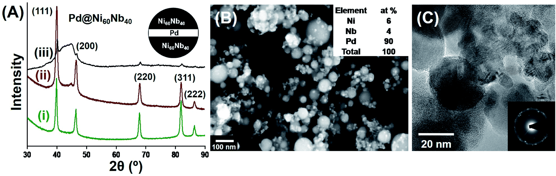 | ||
| Fig. 2 Synthesis of nanocomposite materials using selective area laser scanning on a modified target. Metal (Pd) and alloy (Ni60Nb40) are joined in a fashion shown in the inset of (A). Variation in laser scanning area on Pd (10%, 5% and 1%) produced three different nanocomposite materials (Pd@Ni60Nb40). (A) XRD of these nanocomposite materials are given in (i) to (iii), respectively. As confirmed by SEM (B) and TEM (C) analysis, the as-prepared nanocomposite [from A(i)] is rich in Pd. The inset of (C) shows the SAED pattern of the same nanocomposite. | ||
2.3. Analysis of the amorphous alloy
A detailed characterization of the amorphous Ni60Nb40 nanoparticles and the influence of the laser power has been performed. Three different sets of materials have been prepared using three different values of the laser power (20, 30 and 50 W) from the same Ni60Nb40 target. Fig. S2† shows comparative SEM images (Fig. S2A to C†) and EDX analysis (Fig. S2D to F,† respectively) of the as-synthesized materials. The laser power has an influence on the particle size distribution in the synthesized materials (as evident from Fig. S2A to C†), which will be discussed later. Among the three different materials, the nanopowders synthesized at 20 W laser power were selected for extensive microstructure analysis (as shown in Fig. 3). It was evident from the EDX measurement that the particles retained the atomic composition of the target, measuring 61 at% Ni and 39 at% Nb (Fig. S2D†) compared to 60 at% Ni and 40 at% Nb composition in the target (Fig. 3A(i)). It should be mentioned that the particle sizes are typically larger in the PL-IGC synthesis, if compared to the typical sizes in the range of 5–10 nm as obtained in thermal IGC. In addition, the size distribution of the spherical particles seems to be broader for the PL-IGC process. | ||
| Fig. 3 Microstructural analysis of Ni60Nb40 nanopowder. (A) SEM image of the as-prepared nanopowder. Inset (i) shows EDX of the target. (B) The TEM image shows an amorphous Ni60Nb40 particle (red-circled region) and the SAED pattern of the corresponding sample is shown in the inset. STEM image is shown in (C). (D) and (E) show compositional mapping of Ni and Nb, respectively. RDFs of three regions of the sample are given in (F). RDF of region 1 is calculated from the SAED pattern given in the inset (B). | ||
TEM investigation, including SAED, was carried out and the images are shown in Fig. 3B. Although amorphous phase (highlighted by red circle in Fig. 3B) being majority, SAED pattern suggests mixture of nanocrystallinity in the sample. It should be noted that the presence of a small amount of oxides (oxides of nickel or niobium), was identified by SAED and HRTEM, may contribute to the nanocrystallinity. Additionally, a few larger particles showed good crystallinity and the lattice spacing analysis identified presence of Ni3Nb in the alloy phase. Scanning transmission electron microscopy (STEM) in combination with EDX from different particles also indicate similar compositions for most spheres, regardless to whether they are crystalline or amorphous. Niobium oxide layer could have formed as preferential reactivity of niobium with oxygen leads to amorphous niobium oxide layer on the surface of nickel–niobium alloy material which has been seen before.61 The composition of the sample is determined to be ∼Ni60Nb40 through EDX measurement for a large amount of materials in SEM. STEM-EDX spectrum image in Fig. 2C also indicates homogeneous distribution of nickel and niobium in the sample which is confirmed through the maps presented in Fig. 2D and E, respectively.
In order to gain insight into the local atomic structure of the sample and nanocrystallinity in the sample, three radial distribution functions (RDFs) of the same material is calculated from SAED patterns62 collected from three different regions and shown in Fig. 2F. The RDF of region 1 (blue line) in Fig. 2F is calculated from the SAED pattern given in the inset of Fig. 2B. The other two RDFs corresponding to region 2 and 3 (red and green lines, respectively) are calculated from other regions of the same sample which show similar structures. The RDF features generally agree with the glassy Ni60Nb40 alloy studied before.63 The major peak at 2.54 Å is due to the Ni–Nb bonding.64 The appearance of the smaller peaks around 4.5, 6.5 and 8.5 Å (secondary and higher order packed shells) indicates more ordering in the local atomic structure in the sample compared to metallic glass sample with the same composition.63 The absence of any intensive sharp signal below 2.54 Å confirms that only insignificant amounts of metal–oxygen bonds are present in the sample.
2.4. Tailoring of properties
The influence of different particle sizes and particle size distribution on the structure, i.e., nanocrystallization, and properties was evaluated by ablating at different laser powers. The corresponding XRD patterns of the materials are shown in Fig. 4A. The similar pattern for the three different laser powers used (20, 30 and 50 W) indicate the formation of basically identical amorphous phases in the as-prepared nanopowder. No compositional variation was found in the SEM-EDX analysis (Fig. S2D to F†) among the three different samples. However, the particle size distribution of the three materials (Fig. 4B) shifted to larger average particle sizes with increasing laser power, i.e., the mean value of particle sizes increased gradually from 31.4 nm (at 20 W), 34.6 nm (30 W) to 39.7 nm (50 W) with increase in laser power from 20 W to 50 W, as shown in Fig. 4B. This general trend towards larger particle sizes at high laser power is similar to the observations made by Granqvist and Buhrman for thermal evaporation at increased density of the metal vapor in IGC. In PL-IGC, it is also possible that larger particles are ejected from the target material. The amount of nanocrystals inside the amorphous nanopowder increases with increasing laser power, resulting in changes of the magnetic properties.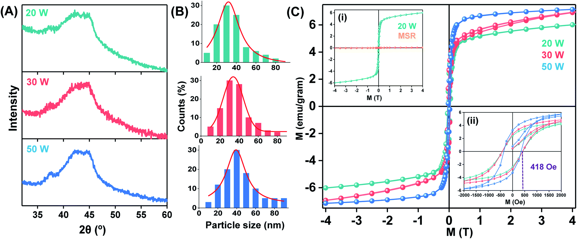 | ||
| Fig. 4 Variation of structure, particle size distribution and magnetic property of the materials with laser power. (A) Ni60Nb40 nanopowders, synthesized using 20, 30 and 50 W laser power, produce similar XRD patterns. Corresponding particle size distributions is given in (B) and average particle size, 31.4 nm (20 W), 34.6 nm (30 W) and 39.7 nm (50 W), respectively was determined. (C) At 5 K, all the materials are ferromagnetic. Analogous MSR showed paramagnetic behavior at 5 K (in inset (i), yellow curve for MSR). The coercive fields of the materials prepared at different laser power are different as shown in inset (ii). | ||
The magnetic behaviour of the samples at different temperatures was measured using SQUID magnetometer. All PL-IGC samples showed ferromagnetic behaviour at 5 K as shown by the hysteresis loops in Fig. 4C. Hysteresis loops recorded in 300 K and 5 K of the sample synthesized at 20 W are shown in Fig. S3.† In order to assess the effect of nanocrystallinity on the magnetism of this material, the magnetic behaviour of a rapidly cooled molten alloy, amorphous Ni60Nb40 (known as melt-spun-ribbon or MSR) was measured at the identical experimental conditions. XRD and SAED pattern shown in Fig. S4† confirmed a perfect amorphous phase in the MSR specimen. When the magnetism at 5 K of the nanopowder (prepared at 20 W) is compared with MSR (inset (i) in Fig. 4C), an increase (about 100 fold) in the overall magnetisation is seen. MSR shows paramagnetic behaviour at 5 K. Clearly, the appearance of ferromagnetic behaviour observed in the nanopowder is due to the contribution from the nanocrystalline phase. It is additionally observed that the nanopowder did not reach saturation magnetisation value even at 4 T, a common behaviour of binary metallic nanoglasses seen before.65
Further analysis on the magnetic ground state of three materials (ablated at 20, 30 and 50 W laser power) at 5 K is shown in Fig. 4C inset (ii). When the M vs. H loops of the samples were compared, alloys synthesized at 20 and 30 W showed 418 Oe coercive filed. Although 15% reduction of coercive field is found (356 Oe), higher saturation magnetisation of the sample was measured for the material synthesized with 50 W power.
The results obtained for the Ni–Nb system demonstrate that the PL-IGC allows for the control of properties, here magnetic, by variation of synthesis parameters.
3. Conclusions
In this report, a custom built pulsed laser inert gas condensation (PL-IGC) system is presented. The system is capable of ablating a wide variety of materials, including low vapor pressure materials, and nanocomposites with great control of the ablation area, ablation time, and laser power. The consequent control of the experimental parameters allows the synthesis of a wide range of pure metals, alloys, oxides and nanocomposites with good yield, precise control over composition and tailoring of materials properties. Using a simple design the PL-IGC system excellent flexibility of the choice of target materials and ablation parameters is offered. Furthermore, the usual parameters of the IGC process, such as gas pressure and type, are employed to control the desired particle sizes and size distributions. The superior performance of the system is demonstrated for metals, alloys and oxides, including nanocomposite material, consisting of a crystalline phase and amorphous phase. In addition, it is demonstrated that properties can be reproducibly controlled by means of the synthesis parameters. In conclusion, some of the shortcomings of thermal evaporation IGC (e.g. restriction to alloys of similar and sufficiently high vapor pressures and low reactivity with the material of the crucibles) and magnetron sputtering IGC (e.g. gas pressure and type suited to sputtering and low yield for oxides) can be overcome by the use of laser ablation. In the future, the integration of in situ compaction to the existing PL-IGC system will further improve the materials as the reactive nanoparticles can be consolidated into dense samples with reduced surface area resulting in minimization of the oxidation of the metastable materials.4. Experimental
A schematic of the custom-built instrument is shown in Fig. 5. The instrument consists of three major components: (a) an infrared picosecond pulsed laser for target ablation, (b) an ultrahigh vacuum chamber where the target is ablated, and (c) a cold finger where the as-synthesized nanoparticles are collected. The technical details are as follows: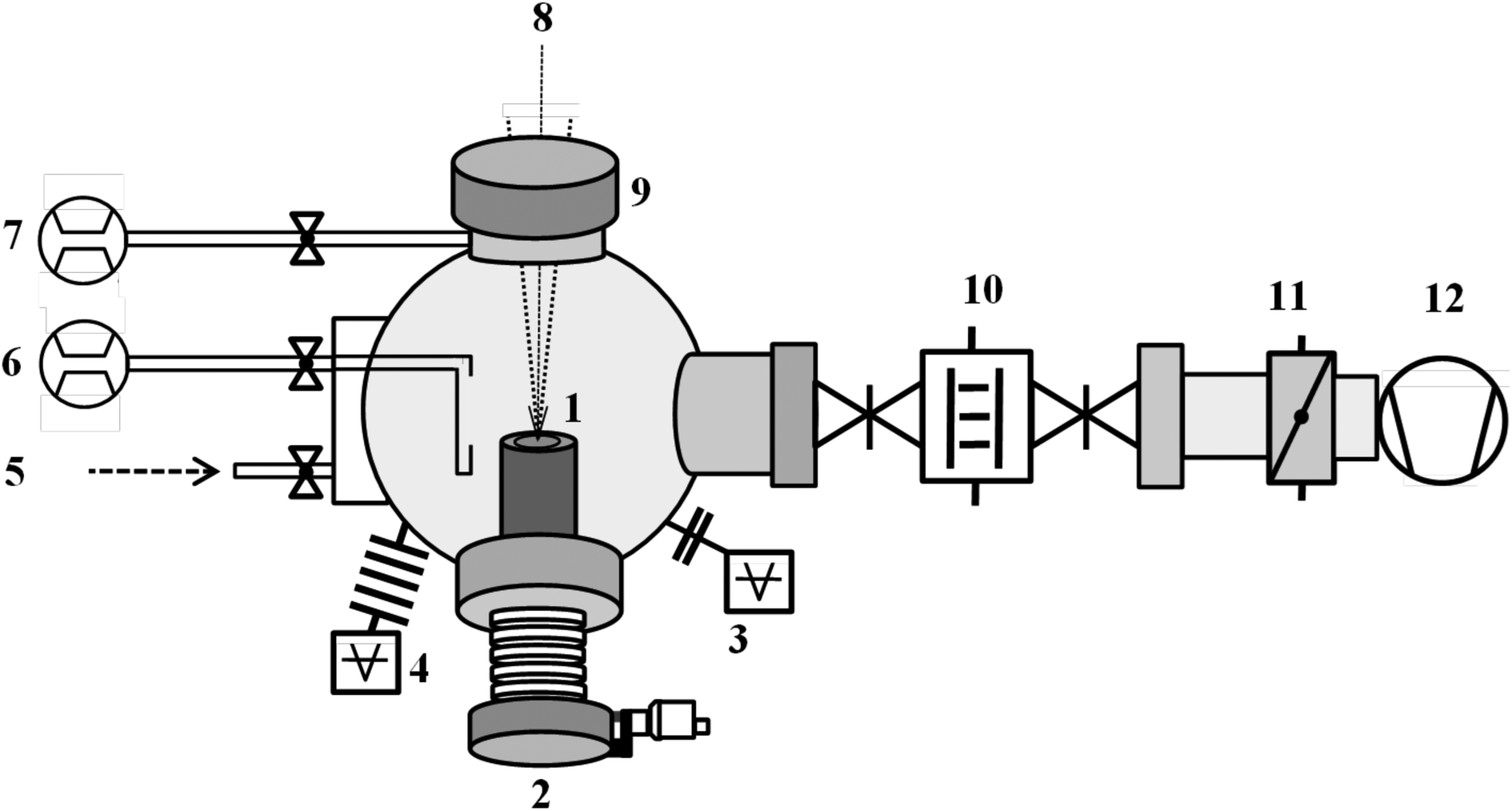 | ||
| Fig. 5 Schematic of the laser ablation chamber. Important components of the chambers are shown. (1) Two-inch diameter target for laser ablation, (2) target mounting z-axis manipulator, (3) Baratron manometer gauge, (4) hot cathode gauge, (5) Swagelok line to inlet inert gas for venting purpose, (6) flow controlled showerhead line, (7) gas line for viewport purging, (8) position of the pulsed laser f-theta lens, (9) viewport with anti-reflection coated BK7 window, (10) liquid nitrogen cold trap to collect ablated nanomaterials, (11) throttle valve, (12) booster pump (130 m3 h−1). Standard vacuum symbols are used in the schematics. | ||
(a) An infrared (IR) pulsed laser (Yb:YAG, wavelength 1030 nm) with maximum output power of 50 watt at 200 or 800 kHz frequency (TRUMPF TruMicro 5000) is used for the ablation process. The beam diameter at the laser exit window is 5 mm. Pulse duration is less than 10 ps with a maximum achievable pulse energy of 250 μJ. Depending on the experimental requirements, different laser irradiance had been used. In case of metallic targets, at 20 watt laser power irradiance was 4.4 × 10¹⁰ W cm−2. At 30 and 50 watt, the irradiance were 4.6 × 10¹⁰ W cm−2 and 5.3 × 10¹⁰ W cm−2, respectively. The laser is directed to the ablation chamber using a series of optical mirrors (Thorlabs) onto two scanning mirrors (Scanlab) mounted on a mobile optical stage (Thorlabs). The scanning mirrors are controlled and operated remotely via a computer-aided design software and are synchronized with the laser. From the mirrors, the laser is focused through the viewport to the target (Fig. 5, item 1) by using an f-theta lens (Q-Optics) having 254 mm focal length. All the optical components and the guiding mirrors along with the laser are placed on a vibration isolated optical bench and placed inside a laser safety box. The custom-built instrument (vacuum assembly, laser and optical mirror assembly) is housed inside a laser secured room with the necessary safety considerations. The diameter of the spot area ablated by the focused laser is found to be 25 μm at 20 W, expanding to 36 μm at the maximum output power (50 W). This range of laser power in combination with an 800 kHz repetition rate has been used to ablate different materials summarized in this work. Uniform laser scan parameters are maintained throughout all synthesis showed in Fig. 1.
Scan area: 1032 mm2
Line spacing: 5 μm
Scanning speed: 4500 mm s−1
Jump speed: 4500 mm s−1
Other parameters (laser power, ablation time) are varied according to the materials and experimental requirements. For example, scan area of 586 mm2 was ablated during synthesis of Pd@Ni60Nb40 (Fig. 2) nanocomposite with different Pd and Ni60Nb40 scan area ratio to produce nanocomposites with different compositions.
(b) The target is mounted on a z-axis manipulator (item 2). A base pressure in the vacuum chamber of approximately 1 × 10⁻⁶ mbar was achieved by means of a side channel high vacuum pump (item 12, Pfeiffer Vacuum, OnTool Booster 150). Using a continuous flow of 500 SCCM He gas (99.9999% purity) through a shower head (vertical slit) and additional 140 SCCM He gas purging (item 6 and 7) around the view port (through which the laser enters into the chamber, item 9) to avoid materials deposition onto the viewport, the gas pressure is maintained at 10 mbar during the entire synthesis. The pressure is regulated by means of a throttle valve (item 11). Several control experiments were performed to understand the effect of laser parameters, partial pressure of gas, ablation time, gas composition etc. on the synthesized materials.
(c) The as-prepared nanopowders are collected using a liquid nitrogen cooled cylinder [typically named cold finger (item 10)], which is placed in between two gate valves. This configuration with closed valves ensures the inert conditions (argon atmosphere) needed to synthesize nanoparticles after the synthesis. The nanopowders, which are typically collected on the cold finger, are transferred under an inert atmosphere (with closed valves) to a glove box [filled with high purity argon (0.1 ppm oxygen, 0.1 ppm water) to avoid surface oxidation] for further processing, such as consolidation and other type of sample preparation for characterization. After each synthesis procedure, the vacuum chamber, view ports, cold finger, etc. were thoroughly cleaned to avoid any cross-contamination from residual materials.
Standard techniques were used to characterize the as-synthesized nanoparticles. All the target materials (except Ni60Nb40 alloy) for the synthesis were 99.9% pure and were purchased from MaTeck GmbH. Ni60Nb40 alloy was received as a gift from Zhejiang University, P. R. China. Structural characterization (XRD) was carried out using a Bruker X-ray diffractometer equipped with a Cu Kα X-ray source. For the XRD characterization, the Ni–Nb amorphous nanopowders were kept inside an airtight dome holder (from Bruker GmbH) to maintain the inert atmosphere to avoid reactions with the ambient atmosphere as much as possible. All other materials were characterized at ambient conditions. Microstructure analysis and materials composition were determined using a Zeiss LEO 1530 scanning electron microscope (SEM) fitted with energy dispersive X-ray (EDX) analyzer. An aberration corrected FEI Titan transmission electron microscope (TEM) operated at 300 kV equipped with a high-resolution spectrometer (Gatan Image Filter Tridiem 965) was used to measure TEM images of the sample. The magnetic measurements were carried out using a superconducting quantum interference device (SQUID) magnetometer of Quantum Design Company. The capsules for magnetic measurement were prepared inside the same glove box mentioned earlier.
Conflicts of interest
There are no conflicts to declare.Acknowledgements
S. B. and A. B. gratefully acknowledge Karlsruhe Institute of Technology for guest scientist fellowships. The authors would like to acknowledge the contribution of Dr Phillip M. Leufke who developed the initial laser ablation setup. A special thanks goes to Prof. Jianzhong Jiang, Department of Materials Science and Engineering, Zhejiang University, Hangzhou, People's Republic of China for providing the Ni60Nb40 target. S. B. and A. B. would like to thank Dr Thomas Reisinger and Dr Christian Kübel for their valuable comments. H. H. is grateful for the financial support provided by the Deutsche Forschungsgemeinschaft under grant HA 1344/30-2.References
- H. Hahn, Nanostruct. Mater., 1997, 9, 3–12 CrossRef CAS.
- I. Michelakaki, S. Stathopoulos, D. Tsoukalas, N. Boukos, D. A. Dragatogiannis and C. A. Charitidis, Beilstein J. Nanotechnol., 2018, 9, 1868–1880 CrossRef CAS PubMed.
- M. R. Chellali, S. H. Nandam, S. Li, M. H. Fawey, E. Moreno-Pineda, L. Velasco, T. Boll, L. Pastewka, R. Kruk, P. Gumbsch and H. Hahn, Acta Mater., 2018, 161, 47–53 CrossRef CAS.
- M. Calizzi, F. Venturi, M. Ponthieu, F. Cuevas, V. Morandi, T. Perkisas, S. Bals and L. Pasquini, Phys. Chem. Chem. Phys., 2016, 18, 141–148 RSC.
- E. Callini, L. Pasquini, L. H. Rude, T. K. Nielsen, T. R. Jensen and E. Bonetti, J. Appl. Phys., 2010, 108, 073513 CrossRef.
- L. Pasquini, A. Barla, A. I. Chumakov, O. Leupold, R. Ruffer, A. Deriu and E. Bonetti, Phys. Rev. B: Condens. Matter Mater. Phys., 2002, 66, 073410 CrossRef.
- L. Pasquini, M. Sacchi, M. Brighi, C. Boelsma, S. Bals, T. Perkisas and B. Dam, Int. J. Hydrogen Energy, 2014, 39, 2115–2123 CrossRef CAS.
- F. Venturi, M. Calizzi, S. Bals, T. Perkisas and L. Pasquini, Mater. Res. Express, 2015, 2, 15007 CrossRef.
- W. A. de Heer, Rev. Mod. Phys., 1993, 65, 611–676 CrossRef CAS.
- P. Melinon, V. Paillard, V. Dupuis, A. Perez, P. Jensen, A. Hoareau, J. P. Perez, J. Tuaillon and M. Broyer, et al. , Int. J. Mod. Phys. B, 1995, 9, 339–397 CrossRef CAS.
- H. Hahn, J. A. Eastman and R. W. Siegel, Ceram. Trans., 1988, 1, 1115–1122 CAS.
- H. Gleiter, Prog. Mater. Sci., 1989, 33, 223–315 CrossRef CAS.
- C. G. Granqvist and R. A. Buhrman, J. Appl. Phys., 1976, 47, 2200–2219 CrossRef CAS.
- W. Hahn and H. Gleiter, Acta Metall., 1981, 29, 601–606 CrossRef CAS.
- R. Birringer, H. Gleiter, H. P. Klein and P. Marquardt, Phys. Lett. A, 1984, 102, 365–369 CrossRef.
- J. X. Fang, U. Vainio, W. Puff, R. Wuerschum, X. L. Wang, D. Wang, M. Ghafari, F. Jiang, J. Sun, H. Hahn and H. Gleiter, Nano Lett., 2012, 12, 458–463 CrossRef CAS PubMed.
- N. Chen, D. Wang, T. Feng, R. Kruk, K.-F. Yao, D. V. Louzguine-Luzgin, H. Hahn and H. Gleiter, Nanoscale, 2015, 7, 6607–6611 RSC.
- J. H. He, H. W. Sheng, P. J. Schilling, C. L. Chien and E. Ma, Phys. Rev. Lett., 2001, 86, 2826–2829 CrossRef CAS PubMed.
- A. Stoesser, M. Ghafari, A. Kilmametov, H. Gleiter, Y. Sakurai, M. Itou, S. Kohara, H. Hahn and S. Kamali, J. Appl. Phys., 2014, 116, 134305 CrossRef.
- H. Hahn and R. S. Averback, J. Appl. Phys., 1990, 67, 1113–1116 CrossRef CAS.
- S. H. Nandam, Y. Ivanisenko, R. Schwaiger, Z. Sniadecki, X. Mu, D. Wang, R. Chellali, T. Boll, A. Kilmametov, T. Bergfeldt, H. Gleiter and H. Hahn, Acta Mater., 2017, 136, 181–189 CrossRef CAS.
- A. Rauf, C. Y. Guo, Y. N. Fang, Z. Yu, B. A. Sun and T. Feng, J. Non-Cryst. Solids, 2018, 498, 95–102 CrossRef CAS.
- Tazuddin, K. Biswas and N. P. Gurao, Mater. Sci. Eng., A, 2016, 657, 224–233 CrossRef CAS.
- W. H. Wang, Prog. Mater. Sci., 2007, 52, 540–596 CrossRef CAS.
- J. F. Loffler, Intermetallics, 2003, 11, 529–540 CrossRef CAS.
- W. L. Johnson, Mater. Sci. Forum, 1996, 225–227, 35–49 CAS.
- A. L. Greer and E. Ma, MRS Bull., 2007, 32, 611–619 CrossRef CAS.
- J. Eckert, J. Das, S. Pauly and C. Duhamel, J. Mater. Res., 2007, 22, 285–301 CrossRef CAS.
- T. V. Kononenko, S. V. Garnov, S. M. Pimenov, V. I. Konov, V. Romano, B. Borsos and H. P. Weber, Appl. Phys. A: Mater. Sci. Process., 2000, 71, 627–631 CrossRef CAS.
- F. Garrelie, F. Bourquard, A.-S. Loir, C. Donnet and J.-P. Colombier, Opt. Laser Technol., 2016, 78, 42–51 CrossRef CAS.
- T. G. Dietz, M. A. Duncan, D. E. Powers and R. E. Smalley, J. Chem. Phys., 1981, 74, 6511–6512 CrossRef CAS.
- P. Lorazo, L. J. Lewis and M. Meunier, Phys. Rev. Lett., 2003, 91, 225502 CrossRef PubMed.
- R. Kelly and A. Miotello, Phys. Rev. E: Stat. Phys., Plasmas, Fluids, Relat. Interdiscip. Top., 1999, 60, 2616–2625 CrossRef CAS PubMed.
- O. Bostanjoglo, R. Niedrig and B. Wedel, J. Appl. Phys., 1994, 76, 3045–3048 CrossRef CAS.
- V. S. Teodorescu, C. Ghica, A. V. Maraloiu, M. Vlaicu, A. Kuncser, M. L. Ciurea, I. Stavarache, A. M. Lepadatu, N. D. Scarisoreanu, A. Andrei, V. Ion and M. Dinescu, Beilstein J. Nanotechnol., 2015, 6, 893–900 CrossRef CAS PubMed.
- A. Abou Chaaya, R. Viter, M. Bechelany, Z. Alute, D. Erts, A. Zalesskaya, K. Kovalevskis, V. Rouessac, V. Smyntyna and P. Miele, Beilstein J. Nanotechnol., 2013, 4, 690–698 CrossRef PubMed.
- A. V. Bulgakov, I. Ozerov and W. Marine, Thin Solid Films, 2004, 453–454, 557–561 CrossRef CAS.
- S. Eliezer, N. Eliaz, E. Grossman, D. Fisher, I. Gouzman, Z. Henis, S. Pecker, Y. Horovitz, M. Fraenkel, S. Maman and Y. Lereah, Phys. Rev. B: Condens. Matter Mater. Phys., 2004, 69, 144119 CrossRef.
- S. Amoruso, G. Ausanio, R. Bruzzese, M. Vitiello and X. Wang, Phys. Rev. B: Condens. Matter Mater. Phys., 2005, 71, 033406 CrossRef.
- T. Yoshida, S. Takeyama, Y. Yamada and K. Mutoh, Appl. Phys. Lett., 1996, 68, 1772–1774 CrossRef CAS.
- M. Kim, S. Osone, T. Kim, H. Higashi and T. Seto, KONA Powder Part. J., 2017, 34, 80–90 CrossRef CAS.
- T. Yoshida, Y. Yamada and T. Orii, J. Appl. Phys., 1998, 83, 5427–5432 CrossRef CAS.
- B. Liu, Z. Hu and Y. Che, Laser Focus World, 2007, vol. 43, pp. 74–78 Search PubMed.
- S. Nolte, C. Momma, H. Jacobs, A. Tunnermann, B. N. Chichkov, B. Wellegehausen and H. Welling, J. Opt. Soc. Am. B, 1997, 14, 2716–2722 CrossRef CAS.
- C.-Y. Shih, M. V. Shugaev, C. Wu and L. V. Zhigilei, J. Phys. Chem. C, 2017, 121, 16549–16567 CrossRef CAS PubMed.
- C.-Y. Shih, R. Streubel, J. Heberle, A. Letzel, M. V. Shugaev, C. Wu, M. Schmidt, B. Gokce, S. Barcikowski and L. V. Zhigilei, Nanoscale, 2018, 10, 6900–6910 RSC.
- D. Perez and L. J. Lewis, Phys. Rev. B: Condens. Matter Mater. Phys., 2003, 67, 184102 CrossRef.
- P. Lorazo, L. J. Lewis and M. Meunier, Phys. Rev. B: Condens. Matter Mater. Phys., 2006, 73, 134108 CrossRef.
- A. Fischer, R. Kruk and H. Hahn, Rev. Sci. Instrum., 2015, 86, 023304 CrossRef CAS PubMed.
- D. Danilov, H. Hahn, H. Gleiter and W. Wenzel, ACS Nano, 2016, 10, 3241–3247 CrossRef CAS PubMed.
- H. Gleiter, Beilstein J. Nanotechnol., 2013, 4, 517–533 CrossRef PubMed.
- A. I. Oreshkin, V. N. Mantsevich, S. V. Savinov, S. I. Oreshkin, V. I. Panov, A. R. Yavari, D. B. Miracle and D. V. Louzguine-Luzgin, Acta Mater., 2013, 61, 5216–5222 CrossRef CAS.
- P. Zhang, Z. Wang, J. H. Perepezko and P. M. Voyles, J. Non-Cryst. Solids, 2018, 491, 133–140 CrossRef CAS.
- Z. Zhu, H. Zhang, D. Pan, W. Sun and Z. Hu, Adv. Eng. Mater., 2006, 8, 953–957 CrossRef CAS.
- G. W. Nieman, J. R. Weertman and R. W. Siegel, Scr. Metall., 1989, 23, 2013–2018 CrossRef CAS.
- U. Diebold, S.-C. Li and M. Schmid, Annu. Rev. Phys. Chem., 2010, 61, 129–148 CrossRef CAS PubMed.
- R. Westerstrom, J. Gustafson, A. Resta, A. Mikkelsen, J. N. Andersen, E. Lundgren, N. Seriani, F. Mittendorfer, M. Schmid, J. Klikovits, P. Varga, M. D. Ackermann, J. W. M. Frenken, N. Kasper and A. Stierle, Phys. Rev. B: Condens. Matter Mater. Phys., 2007, 76, 155410 CrossRef.
- V. Sittinger, F. Ruske, W. Werner, C. Jacobs, B. Szyszka and D. J. Christie, Thin Solid Films, 2008, 516, 5847–5859 CrossRef CAS.
- T. Loeffler, A. Savan, A. Garzon-Manjon, M. Meischein, C. Scheu, A. Ludwig and W. Schuhmann, ACS Energy Lett., 2019, 4, 1206–1214 CrossRef CAS.
- E. J. Pickering and N. G. Jones, Int. Mater. Rev., 2016, 61, 183–202 CrossRef CAS.
- A. S. Trifonov, A. V. Lubenchenko, V. I. Polkin, A. B. Pavolotsky, S. V. Ketov and D. V. Louzguine-Luzgin, J. Appl. Phys., 2015, 117, 125704 CrossRef.
- X. Mu, D. Wang, T. Feng and C. Kuebel, Ultramicroscopy, 2016, 168, 1–6 CrossRef CAS PubMed.
- L. Yang, X.-f. Meng and G.-q. Guo, J. Mater. Res., 2013, 28, 3170–3176 CrossRef CAS.
- H. Oji, K. Handa, J. Ide, T. Honma, S. Yamaura, A. Inoue, N. Umesaki, S. Emura and M. Fukuhara, J. Appl. Phys., 2009, 105, 113527 CrossRef.
- R. Witte, T. Feng, J. X. Fang, A. Fischer, M. Ghafari, R. Kruk, R. A. Brand, D. Wang, H. Hahn and H. Gleiter, Appl. Phys. Lett., 2013, 103, 073106 CrossRef.
Footnotes |
| † Electronic supplementary information (ESI) available. See DOI: 10.1039/c9na00533a |
| ‡ These authors contributed equally. |
| This journal is © The Royal Society of Chemistry 2019 |