
 Open Access Article
 This Open Access Article is licensed under a Creative Commons Attribution-Non Commercial 3.0 Unported Licence
Evolution of inter-layer coupling in artificially stacked bilayer MoS2†
Suman
Sarkar
a,
H. L.
Pradeepa
a,
Goutham
Nayak
b,
Laetitia
Marty
b,
Julien
Renard
b,
Johann
Coraux
b,
Nedjma
Bendiab
b,
Vincent
Bouchiat
b,
Jaydeep K.
Basu
 a and
Aveek
Bid
*a
a and
Aveek
Bid
*a
aDepartment of Physics, Indian Institute of Science, Bangalore 560012, India. E-mail: aveek@iisc.ac.in
bUniv. Grenoble Alpes, CNRS, Grenoble INP, Institut Néel, 38000 Grenoble, France
First published on 2nd October 2019
Abstract
In this paper, we show experimentally that for van der Waals heterostructures (vdWh) of atomically-thin materials, the hybridization of bands of adjacent layers is possible only for ultra-clean interfaces. This we achieve through a detailed experimental study of the effect of interfacial separation and adsorbate content on the photoluminescence emission and Raman spectra of ultra-thin vdWh. For vdWh with atomically-clean interfaces, we find the emergence of novel vibrational Raman-active modes whose optical signatures differ significantly from that of the constituent layers. Additionally, we find for such systems a significant modification of the photoluminescence emission spectra with the appearance of peaks whose strength and intensity directly correlate with the inter-layer coupling strength. Our ability to control the intensity of the photoluminescence emission led to the observation of detailed optical features like indirect-band peaks. Our study establishes that it is possible to engineer atomically-thin van der Waals heterostructures with desired optical properties by controlling the inter-layer spacing, and consequently the inter-layer coupling between the constituent layers.
1 Introduction
The isolation of single-layer two-dimensional (2D) materials1–3 and the ability to assemble them into van der Waals heterostructures (vdWh)4 is of great current interest both from an academic as well as an applied point of view. The ability to deterministically stack atomic layers of 2D materials with a disparate range of properties5 – Dirac semi-metals, semiconductors,3 superconductors,6 ferromagnets and insulators7 has opened up the possibility of creating artificial systems with properties not found in the constituent layers. This has led to predictions of devices with a variety of applications – flexible high speed electronics,8,9 high fidelity sensors,10 fast optical switches,11 photo-detectors,12–14 and solar cells15 to name just a few. From an academic perspective, the hybridization of the bands of the constituent layers give rise to emergent phenomenon absent in the parent materials – a few cases in point being the observation of spin-split bands in single layer-graphene on WSe2,16 the discovery of superconductivity in artificial twisted bilayer-graphene6,17–19 and evidence for moiré excitons in vdWh.20–23The steric repulsion between the layers makes the stacking arrangement strongly dependent on the inter-layer coupling strength which affects all physical properties of the system.24 Several studies have shown that the formation of vdWh strongly affects the phonon-spectrum, strength of electron-phonon interaction and the phonon–phonon interactions in both the constituent layers as well as in the vdWh.25,26 The inter-layer coupling between the constituent layers was found to depend sensitively on their relative twist angle which strongly affects the low-frequency Raman modes27 as well as the relative contribution of the excitonic and trionic channels to the photoluminescence (PL) intensity.25,28 The twist angle also determines the moiré potential generated in these twisted bilayers which have been shown to produce additional phonons in the constituent monolayers leading to the emergence of Raman modes corresponding to the zone-center phonons in the vdWh.26 On the other hand, it was shown that the twist angle did not have any significant effect on the electronic band gap29 or on the high-frequency intra-layer Raman modes.27
Although there have been a series of recent studies exploring the tunability of inter-layer coupling strength with twist angles in vdWh, corresponding studies of its dependence on inter-layer spacing in atomically-thin heterostructures is missing. For these vdWh-based devices to manifest their intrinsic properties,30 it is essential that the constituent layers be in intimate physical contact with each other as the relevant interactions fall off exponentially with distance. It is thus possible, in principle, to engineer vdWh with desired optical properties by controlling the inter-layer spacing, and consequently the inter-layer coupling between the constituent layers.
A major obstacle in practically achieving this is the difficulty in reproducibly fabricating vdWh with atomically clean interfaces. Most groups report the occurrence of so-called ‘blisters’ or ‘bubbles’31 between the layers due to the presence of adsorbate on the individual layers (typically polymer residue and airborne adsorbed species) or due to non-co-laminated transfer of one layer over the other.32,33 These bubbles determine how close the layers can approach each other which in turn governs the inter-layer coupling strength. Raman spectroscopy reveals the appearance of multiple low-frequency breathing modes which were interpreted to indicate non-uniform coupling across the interface27 and the complete absence of these modes in dirty interfaces show that inter-layer breathing modes can only be generated in vdWh regions with atomically clean interfaces.25 Gomez et al. have shown that in artificially stacked MoS2 structure the coupling between the constituent layers depends on how the stacks are prepared.34 When the artificial stacks were prepared by folding a single layer of MoS2, the Raman spectra showed strong inter-layer coupling. The PL spectra showed an additional peak which was attributed to be due to the emergence of a luminescence feature corresponding to electron–hole recombination across an indirect band-gap which confirms the bilayer nature of the stack.34,35 On the other hand, for stacks made from two independent layers transferred on top of each other, no inter-layer coupling mode was observed in the Raman spectra, neither was the indirect band-gap feature observed in PL.35 Surprisingly, in both cases, the stacks showed PL intensity comparable to constituent monolayers which were attributed, at least partially, to the fact that as prepared artificial bilayers can have a varying degree of inter-layer coupling depending on the distance between the layers. It is thus very important to probe the dependence of inter-layer coupling in vdWh on the interface quality.
Here we probe the evolution of optical properties of 2D transition metal dichalcogenide (TMD) based layered devices – from essentially decoupled single-layers to strongly coupled heterostructures. Using MoS2 as a model system, we studied the PL and Raman spectra of multiple samples of individual single-layer (SL), natural bilayer (NBL) and artificial bilayer (ABL) at ambient temperature and pressure. High-frequency Raman (here high frequency refers to the range 200–500 cm−1) studies probe the evolution of intra-layer in-plane and out-of-plane symmetric vibrational modes with layer coupling strength [Fig. 1(b)]. From low frequency Raman spectroscopy one can identify the number of layers and the strength of inter-layer coupling in artificially stacked layers.27 PL provides insight about direct optical gap, indicates the presence of indirect band gap which depends on the degree of inter-layer electronic coupling [Fig. 1(c)] and helps identify the excitonic and trionic transition levels [Fig. 1(d)]. We find that the presence of bubbles at the interface between two individual layers effectively decouples the constituent layers. Post-thermal annealing, the photoluminescence of ABL MoS2 gets quenched and an indirect band-gap excitonic peak appears. The difference between the E′ and  Raman modes increases approaching that of NBL MoS2 and an inter-layer breathing mode appears in the low-frequency Raman spectra. These observations indicate that it is possible to prepare vdWh heterostructures with strong coupling between the individual monolayers opening up the way to probe the predicted intrinsic properties of vdWh.
 | ||
Fig. 1 (a) Schematic crystal structure of MoS2. (b) Intra-layer Raman active modes and inter-layer breathing mode and shear mode of MoS2 crystal. (c) Band structure of SL and NBL MoS2 showing direct band gap and indirect band-gap respectively. (d) Schematic band diagram of SL MoS2 representing the trionic, A- and B-excitonic transitions at the K point of the Brillouin zone. (e) Optical image of sample 1, showing the two constituent SL (outlined by red lines), the ABL region (outlined by black line), NBL (outlined by green line) and the artificial trilayer, ATL (outlined by white line). The low-frequency Raman spectra were collected along the dotted red line. (f) PL intensity map of sample 1 (integrated over the energy range 1.7–2.1 eV) showing intensity enhancement in the ABL over the SL or NBL. (g) PL spectra of SL (black line), ABL (red line), and NBL (green line) MoS2. (h) High frequency Raman spectrum of SL (black line), ABL (red line) and NBL (green line) MoS2 showing the E′ and  (for SL) and E2g and A1g (for NBL and ABL) peaks. (i) High frequency Raman shift δω measured at several locations in SL, ABL and NBL regions. All the data presented in panels (e–i) are for the pre-annealed sample. (for SL) and E2g and A1g (for NBL and ABL) peaks. (i) High frequency Raman shift δω measured at several locations in SL, ABL and NBL regions. All the data presented in panels (e–i) are for the pre-annealed sample. | ||
2 Experimental details
We used a dry-transfer method to prepare samples of MoS2 on 290 nm SiO2/Si++ substrates.33,36–38 SL, NBL and multi-layer flakes of MoS2 were mechanically exfoliated from single crystals of naturally occurring MoS2 (SPI supplies®) using scotch tape on silicon-based organic polymer polydimethylsiloxane (PDMS) films purchased from GEL-PACK®. The flakes were then sequentially transferred from PDMS onto SiO2/Si++ substrates under an optical microscope (50X objective) using a home-built transfer set-up based on Thorlabs 3-Axis linear translation stage (MTS-Z8). The lateral speed of the stages was limited to less than 1 μm s−1 to avoid physical damage to the flakes. After the transfer, the PDMS film was removed very slowly to avoid wrinkling or tearing of the flakes. The number of layer was identified from their optical colour contrast and subsequently confirmed from Raman spectra and direct height measurements using atomic force microscope.39Photoluminescence and Raman spectroscopy measurements were done in two separate confocal microscope based set-up. One of them had a spatial resolution of 350 nm and used a 532 nm laser source for both PL measurements and Raman-spectroscopy. The PL and Raman spectra were recorded using 600 lines per mm and 1800 lines per mm gratings respectively. The other system had a spatial resolution of 500 nm and used a 514 nm laser source. In this system the PL and Raman spectra were recorded using 300 lines per mm and 1800 lines per mm gratings respectively. In both cases the laser power levels were kept very low (∼100 μW) to avoid sample heating. All the data were collected under ambient conditions at 25 °C and at a humidity level of ∼45%.
3 Results and discussions
An optical image of an as-prepared ABL sample (sample 1) is shown in Fig. 1(e). It shows the two pristine SL MoS2 flakes and the ABL formed by their overlap in the central region. Fig. 1(f) shows the integrated PL intensity mapping of the sample over the energy range of 1.7–2.1 eV, the color bar showing the total PL count over this energy window. The PL spectrum is dominated by pronounced peaks characteristic of excitonic transitions (Fig. 1(g)). The two main features at ∼1.92 eV and ∼2.08 eV, conventionally labeled as A and B peaks, arise from direct excitonic transitions between the highest levels of the spin–orbit interaction induced spin-split valence band and the bottom of the conduction band.39 Both Fig. 1(f) and (g) establish the PL intensity of the ABL region to be significantly higher than that of the constituent pristine SL, in direct contrast to previous reports.34Fig. 2(a) shows the PL map taken on another sample (sample 2). Similar to sample 1, we find a large enhancement of the PL intensity in the ABL region (marked by a green dotted line) as compared to the SL (marked by a black dotted line). A careful inspection of the optical image (Fig. 2(c)) of the as-prepared sample shows the presence of a large number of bubbles in the ABL. The sample was then annealed at 400 °C. The annealing temperature was reached by heating the sample inside a quartz tube in 10−6 mbar pressure, at the rate of 5 °C per minute. The sample was maintained at the desired temperature for two hours. It was then cooled down to room temperature at the same rate and taken out of the annealing chamber after venting the quartz tube with 99.99% pure nitrogen gas. Vacuum annealing at pressure 10−6 mbar at 400 °C led to an almost complete cleansing of the contaminants from in-between the layers leading to a disappearance of the bubbles (Fig. 2(d)). Simultaneously, the PL intensity of the post-annealed ABL was reduced to a value much lower than that of the SL. From Fig. 2(b) and (d) we can find an almost one-to-one correspondence between the locations of residual bubbles in the ABL and the regions of enhanced PL intensity. This was seen clearly in AFM surface topography (Fig. 2(d) inset) which indicates the presence of bubbles exactly at those locations where the PL enhancement was retained in the ABL even after the annealing step. Fig. 3 compares the PL spectra of the sample 2 before and after annealing. We find that for the as-prepared device, the ABL region has almost 2.5 times higher PL intensity than that in the SL regions and almost 5 times higher intensity than that of an adjacent NBL region. After annealing, the PL intensity of the ABL is quenched and it matches with that of the neighboring NBL MoS2. The spectral decomposition of the PL intensity of the ABL before and after annealing shows significant differences (Fig. 3[(c) and (d)]). The annealing process suppressed the relative contribution of the trion peak while enhancing that of the A-exciton.34 Both the excitonic and trionic peak positions got red-shifted while the change in the peak widths did not seem to follow any particular pattern. An interesting observation is the appearance of an additional peak at 1.64 eV in the ABL post-annealing (Fig. 3(d)). This was identified as an ‘indirect peak’ arising due to transition across the indirect band-gap.40 The fact that it is seen only in the annealed device shows that annealing significantly increases the inter-layer coupling in the ABL.
 | ||
| Fig. 2 PL intensity map (integrated over the energy range 1.5–2.1 eV) of sample 2 (a) as-fabricated and (b) post-annealing at 400 °C. The ABL region is marked by green dashed lines while the SL region is marked by black dashed lines. The colour bars represent the total integrated PL counts on the CCD camera over the range 1.5–2.1 eV. The corresponding optical micrographs are shown in (c) and (d) respectively. The ABL is marked with red dashed line while the SL region is marked with black dashed line. The inset of (d) shows an AFM image of a small portion of the ABL region post-annealing. (e) An AFM topography of the stack. (f) Line-scan showing the height of the bubbles in the region marked with white-dashed lines in the AFM image in (e). | ||
 | ||
| Fig. 3 PL spectra of sample 2 before and after annealing at 400 °C. (a) PL intensity of the SL (red open circles), ABL (blue open circles) and NBL (green open circles) before annealing. Inset: PL mapping of the sample before annealing. (b) PL intensity of the SL (red open circles), ABL (blue open circles) and NBL (green open circles) after annealing. Inset: PL mapping of the sample after annealing. (c) Spectral decomposition of the ABL PL spectrum acquired before annealing – the spectrum has been fitted with three Lorentzian peaks corresponding to trion, A-exciton and B-exciton peaks. (d) Spectral decomposition of the ABL PL spectrum acquired after annealing fitted with four Lorentzian peaks corresponding to indirect transition, trion, A-exciton and B-exciton peaks. | ||
It was observed that although vacuum annealing at 400 °C very effectively cleaned up the bubbles created during the process of formation of these ABL, it also led to structural damage of the sample [see Fig. S1 and S2 in ESI S1 and S2† respectively]. To determine the optimum condition for the preparation of bubble-free ABL, we annealed a series of samples at different temperatures – recording the optical image, PL and Raman spectra after each annealing step. In this case of ambient annealing, the sample was heated at 10 °C per minute to the desired annealing temperature and maintained there for 10 minutes. It was cooled down at 10 °C per minute to 25 °C and measured the results for one such sample (sample 3) are presented in Fig. 4. Annealing at temperatures less than 200 °C did not have any significant effect on the concentration of the bubbles. Annealing at temperatures between 200 °C and 300 °C led to significant cleansing of the contaminants present at the interface and consequent disappearance of the bubbles. We noticed that these contaminants tended to accumulate in some particular places and form few prominent bubbles leaving the rest of the sample clean. This increased the transparency of the stack as seen from the optical images. Concurrently, the PL intensity got quenched showing that the inter-layer coupling strength gradually increased as the layers came closer together. The bubbles remaining even after the annealing treatment can be seen to give rise to localized PL enhancement whose locations can be correlated with those of the bubbles seen in optical images. Annealing at T ≥ 400 °C led to severe physical damage of the sample. Details regarding the optimal temperature and environment for annealing are provided in ESI S1.†
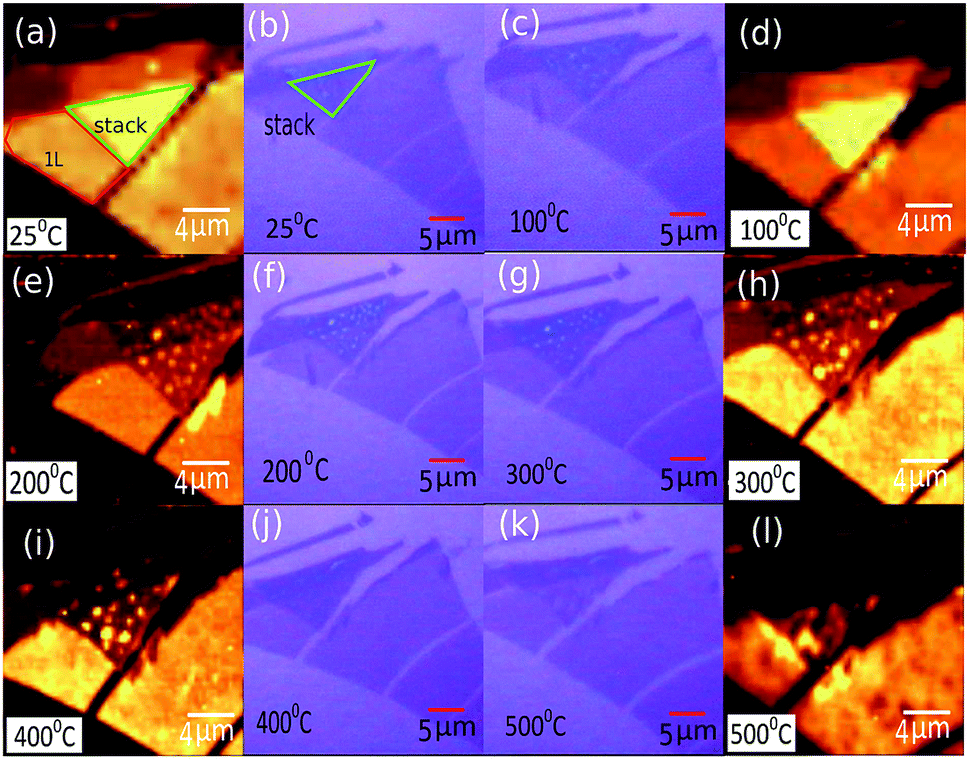 | ||
| Fig. 4 Optical images and the corresponding PL intensity maps of MoS2 sample after annealing at different temperatures: 25 °C, 100 °C, 200 °C, 300 °C, 400 °C and 500 °C. The ABL region in (a) and (b) are marked with green solid lines as a visual guide. The red solid line in (a) marks the SL. | ||
A careful study of Raman spectra can yield a wealth of information regarding the doping-level and strain present in a sample. Ultra-thin 2D materials are extremely sensitive to substrate interactions as these can lead to structural modifications.41,42 This produces inhomogeneities in as-fabricated vdWh which cause spatial variations of strain and doping in the sample. Electronic doping modifies the occupation in the conduction band which in turn affects electron-phonon coupling (EPC) of the Raman modes.43 High-frequency Raman spectrum44 of SL MoS2 consists of two prominent modes – E′ and  [see Fig. 1(b)]. The E′ mode arises from in-plane anti-phase oscillations of the Mo and S atoms while the
  mode is due to the out-of-plane anti-phase oscillations of the sulphur atoms.45 To clarify, following accepted conventions we have used the notation E′ and
  for SL sample and E2g and A1g for the NBL and ABL sample. Fig. 1(h) shows a representative Raman spectrum of sample 1 pre-annealing. Both the peaks are present in all the regions (SL, NBL and ABL) although their spectral positions vary. As shown in Fig. 1(i), the value of the frequency difference
 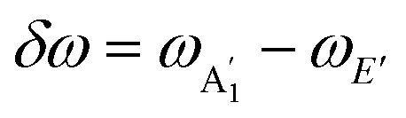 between these two modes in both the SL as well as in the ABL regions (δω ∼ 19.5–20.0 cm−1) is lower than that of NBL (δω ∼ 21.0 cm−1). δω depends critically on the number of layers and is a measure of the inter-layer interaction strength.46 As shown previously27 it is almost independent of the twist angle in the vdWh. The fact that our unannealed artificial ABL has Raman spectra characteristic of SL suggests that the two layers are effectively decoupled corroborating our conclusions from PL study.
EPC is much higher for the out-of-plane  breathing mode (due to orbital overlap) than the in-plane vibrational mode E′. So it is to be expected that doping will induce significant Raman shift in the
  mode while leaving E′ almost unaffected.43 In the low charge impurity and low strain limit, these two effects, viz. strain and doping can be considered as decoupled factors affecting the Raman shift.47,48 This allows a linear transformation from peak position to strain and doping density. The mean value of the phonon mode frequency is usually taken to be the unperturbed value. Thus, a 2D plot of the position of the Raman modes can provide quantitative information about the biaxial strain as well as the charge impurity concentration (induced either due to the presence of substrate49 or by the accumulation of adsorbates between the layers during the mechanical transfer process50).
Such a plot for our sample 1 is shown in Fig. 5. To obtain the strain and charge density, we use the mean values of the Gruneisen parameter due to strain −0.86 for E′ and 0.15 for  .51 We also use, as calibration, the reported Raman shift of 4 cm−1 and 0.6 cm−1 for
  and E′ mode respectively for electron concentration 1.8 × 1013 cm−2.43 The inclined vertical solid lines in the figure represent iso-strain lines with 0.1% increment in strain. The inclined horizontal parallel dotted lines are the iso-doping lines with a spacing of 5 × 1012 cm−2. In this plot, every data point represents the peak position at different locations of the sample obtained by spatially resolved Raman mapping. We observe that SL and pre-annealed ABL has almost the same amount of strain and charge impurity concentrations (see the light-blue shaded region in the plot). This shows that for pre-annealed stack, the constituent layers maintain their intrinsic properties and are decoupled.
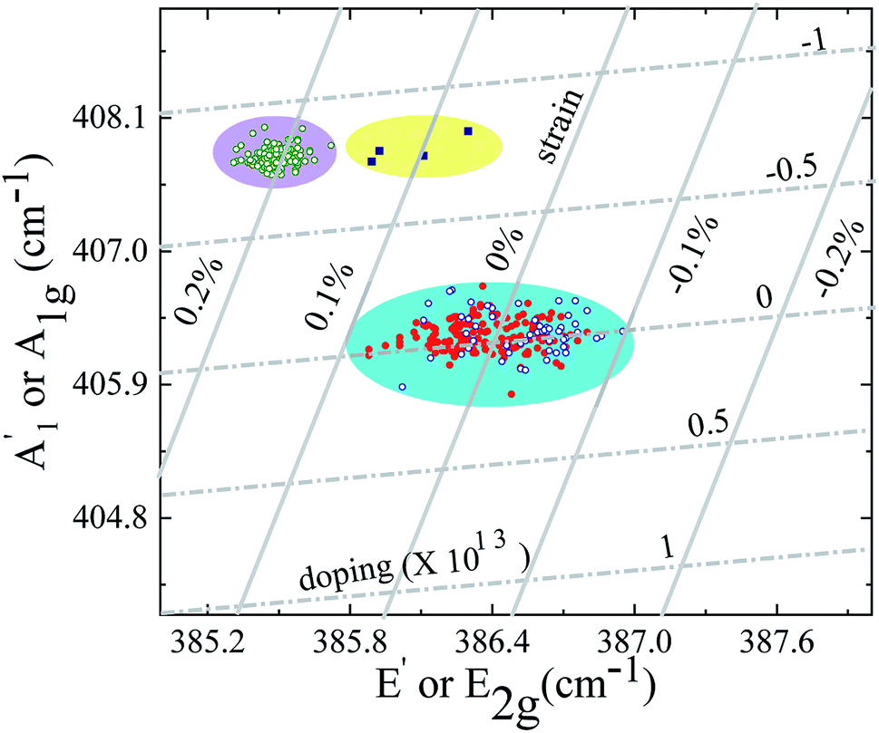 | ||
Fig. 5 Plot of peak position of A1g (or  ) with peak position of E2g (or E′) for SL (blue open circle), NBL (green open circle), pre-annealed ABL (red filled circle) and post-annealed ABL (blue solid square). Inclined vertical solid lines and inclined horizontal dotted lines are equidistant lines representing iso-strain and iso-doping lines respectively. The origin of these two doping and strain axes were determined from the mean value of the peak position of E2g and A1g peak of SL (see text for details). The spacing between the iso-strain lines is 0.1% and spacing between iso-doping lines is 5 × 1012 cm−2. ) with peak position of E2g (or E′) for SL (blue open circle), NBL (green open circle), pre-annealed ABL (red filled circle) and post-annealed ABL (blue solid square). Inclined vertical solid lines and inclined horizontal dotted lines are equidistant lines representing iso-strain and iso-doping lines respectively. The origin of these two doping and strain axes were determined from the mean value of the peak position of E2g and A1g peak of SL (see text for details). The spacing between the iso-strain lines is 0.1% and spacing between iso-doping lines is 5 × 1012 cm−2. | ||
The maximum amount of strain developed in the SL and pre-annealed ABL system is less than 0.1% and the maximum charge impurity concentration is within ± 2.5 × 1012 cm−2. After annealing, the Raman peak positions get shifted –  peak has a blue-shift of about 2.2 cm−1 while E′ has a maximum red-shift of about 1 cm−1. This moves the post-annealed ABL (yellow shaded region in Fig. 5) closer to the NBL in the peak-position diagram (pink shaded region in Fig. 5). This change in the spectral position of the ABL Raman modes – from single-layer-like to bilayer-like – indicates that post-annealing there is an increase in the inter-layer coupling strength leading to a modification of the band structure. Thus, after annealing the constituent layers are no more decoupled from each other – rather they form a coupled bilayer system. It should be noted that while the
  peak position for ABL matches very well with of the NBL post-annealing, the E′ peak in the annealed ABL is still slightly blue shifted (by about 0.4 cm−1) with respect to that of the NBL. We argue that this difference between NBL and ABL arises due to arbitrary angle stacking in the ABL. We come back to this point later while discussing the low-frequency Raman modes.
Low frequency Raman modes in 2D transition metal dichalcogenides are known to be very sensitive to the inter-layer coupling strength.27,50 Measurements on NBL flakes show inter-layer in-plane shearing mode at 22.3 cm−1 and out-of-plane breathing mode at 40.5 cm−1 while these are absent in SL flakes.27 Our measurements indicate that before annealing the ABL does not show any of these modes and its low-frequency Raman spectra is similar to that of an SL (Fig. 6(a)). Post-annealing, an out-of-plane breathing mode develops at 35 cm−1 (Fig. 6(b)) which is frequency shifted by about 5 cm−1 as compared to NBL MoS2. We confirmed that the position of this mode is the same throughout the ABL region. As an example, in Fig. 6(b) we show the average of a line-scan taken across the sample along the line shown by red dotted line in Fig. 1(e) – the average spectrum (shown by the blue solid line) matches very well with the individual spectrum taken at a different location on the sample (shown in green filled circles). The appearance of the low-frequency out-of-plane breathing mode again confirms the enhancement of inter-layer coupling post-annealing.
 | ||
| Fig. 6 (a) Low frequency Raman spectra of SL, NBL and ABL pre-annealing and (b) post-annealing. Light gray and dark gray shaded regions represent the low-frequency shear-mode and low-frequency breathing mode regions respectively. Note that, in contrast to NBL, for SL and ABL both the breathing as well as the shear modes are absent in the pre-annealed sample. Post-annealing, the out-of-plane breathing mode appears in the ABL while the shear mode still remains absent. The blue solid line is the average low frequency Raman spectra measured on the ABL sample along the red dotted line in (Fig. 1(e)). | ||
We do not observe the inter-layer in-plane shearing mode in post-annealed ABL, this is consistent with theoretical predictions.52,53 Below we discuss the possible cause for this absence of the shearing mode. The ABL stacks have an arbitrary twist angle. Consequently, they do not have any high symmetry orientation and their inter-atomic layer distance is larger than in the 2H phase. This makes the force between the adjacent layers small and the inter-layer shearing mode energy very low. This leads to low shear mode frequency and intensity in artificially stacked MoS2. This is in line with our observation that while for high-frequency Raman modes, the breathing mode peak  peak position for NBL matches very well with of the ABL after annealing, the shear mode E′ peak in the annealed ABL is blue-shifted with respect to the NBL. The estimated Raman shift for the shear mode is ∼1.8 cm−1ref. 53 and 54 which is below the Rayleigh cut-off of ∼18 cm−1 of the instrument. Note that the absence of inter-layer shear mode cannot be because of the relative orientation of the stacks with the polarization of light as the same set-up could detect the low-frequency shear mode for NBL and in few-layer MoS2 samples. The absence of the low-frequency inter-layer shear mode was also noted in MoSe2 twisted-bilayers and was again attributed to unaligned stacking leading to an absence of in-plane restoring force.55,56
4 Conclusions
We note that the effect of annealing on optical properties of TMDC heterostructures has been studied before – see for example.57–59 However, our study differs from that of previous workers in several significant ways. We have provided a detailed comparison between the pre-annealed and post-annealed condition for artificially stacked MoS2 and show that post-annealing, the PL intensity approached that of natural bilayer MoS2. Post-annealing we find the appearance of the low-energy indirect peak. We show the evolution of individual in-plane and out-of-plane Raman modes with annealing. These phenomenon cannot be studied in artificial heterostructures like MoSe2–WSe2 (on which most of the previous studies were performed) due to lack of a naturally available standard to compare against like NBL MoS2. Furthermore, we study the evolution of low-frequency Raman modes pre- and post-annealing. We report and explain the appearance of layer breathing mode and the absence of shear mode in ABL MoS2 after annealing – both these modes are present in NBL MoS2.To conclude, through a systematic study of PL emission and Raman spectra, we explored the dependence of inter-layer coupling strength on the relative separation between the constituent layers of vdWh with atomically-clean interfaces. We establish that it is possible to engineer vdWh with desired optical properties by controlling the inter-layer spacing, and consequently the inter-layer coupling between the constituent layers. We provide a recipe to achieve this in vdWh of TMD as well as of other 2D materials (see ESI† for data on other heterostructures). In heterostructures with ultra-clean interfaces, we find the appearance of a low-frequency Raman-active inter-layer breathing mode which we interpret to indicate strong inter-layer coupling strength. We found that high-frequency Raman shift also follows the evolution from SL to NBL after annealing in ABL sample. We establish that inter-layer separation can be used as a handle to tune both the PL emission intensity and peak-positions. While PL enhancement is exciting from a technological applications perspective, its quenching led us to the observation of detailed optical features like an indirect-band peak. We use the PL spectra to quantify the strain and doping levels in these heterostructures both pre- and post-annealing. Additionally, we observed that once the vdWh are treated to achieve atomically-clean interfaces, they remain optically [see S3 of ESI†] and electronically stable60 over several months making them suitable for long term studies and practical applications. These observations bring TMD-based heterostructures one-step closer to the predicted optoelectronic applications.
Conflicts of interest
There are no conflicts to declare.Acknowledgements
A. B. and J. K. B. acknowledge financial support from SERB, DST, Govt. of India; Nanomission, DST, Govt. of India and support under FIST program, DST. A. B, G. N. and V. B. acknowledge funding from the Indo-French Centre for the Promotion of Advanced Research (CEFIPRA) (project No. 5304-F). We acknowledge fruitful discussions with Mit Nayak, Indrajit Maity and Manish Jain regarding the band-structure and low-frequency Raman modes of SL and NBL MoS2.Notes and references
- H. Li, Q. Zhang, C. C. R. Yap, B. K. Tay, T. H. T. Edwin, A. Olivier and D. Baillargeat, Adv. Funct. Mater., 2012, 22, 1385–1390 CrossRef CAS.
- K. S. Novoselov, A. K. Geim, S. V. Morozov, D. Jiang, Y. Zhang, S. V. Dubonos, I. V. Grigorieva and A. A. Firsov, Science, 2004, 306, 666–669 CrossRef CAS.
- B. Radisavljevic, A. Radenovic, J. Brivio, I. V. Giacometti and A. Kis, Nat. Nanotechnol., 2011, 6, 147 CrossRef CAS PubMed.
- C. R. Dean, A. F. Young, I. Meric, C. Lee, L. Wang, S. Sorgenfrei, K. Watanabe, T. Taniguchi, P. Kim, K. L. Shepard and J. Hone, Nat. Nanotechnol., 2010, 5, 722 CrossRef CAS.
- S. Z. Butler, S. M. Hollen, L. Cao, Y. Cui, J. A. Gupta, H. R. Gutiérrez, T. F. Heinz, S. S. Hong, J. Huang, A. F. Ismach, E. Johnston-Halperin, M. Kuno, V. V. Plashnitsa, R. D. Robinson, R. S. Ruoff, S. Salahuddin, J. Shan, L. Shi, M. G. Spencer, M. Terrones, W. Windl and J. E. Goldberger, ACS Nano, 2013, 7, 2898–2926 CrossRef CAS PubMed.
- Y. Cao, V. Fatemi, S. Fang, K. Watanabe, T. Taniguchi, E. Kaxiras and P. Jarillo-Herrero, Nature, 2018, 556, 43 CrossRef CAS PubMed.
- Z. Lin, B. R. Carvalho, E. Kahn, R. Lv, R. Rao, H. Terrones, M. A. Pimenta and M. Terrones, 2D Materials, 2016, 3, 022002 CrossRef.
- G.-H. Lee, Y.-J. Yu, X. Cui, N. Petrone, C.-H. Lee, M. S. Choi, D.-Y. Lee, C. Lee, W. J. Yoo, K. Watanabe, T. Taniguchi, C. Nuckolls, P. Kim and J. Hone, ACS Nano, 2013, 7, 7931–7936 CrossRef CAS PubMed.
- G. Eda, H. Yamaguchi, D. Voiry, T. Fujita, M. Chen and M. Chhowalla, Nano Lett., 2011, 11, 5111–5116 CrossRef CAS PubMed.
- D. Kufer and G. Konstantatos, Nano Lett., 2015, 15, 7307–7313 CrossRef CAS PubMed.
- F. Koppens, T. Mueller, P. Avouris, A. Ferrari, M. Vitiello and M. Polini, Nat. Nanotechnol., 2014, 9, 780 CrossRef CAS.
- O. Lopez-Sanchez, D. Lembke, M. Kayci, A. Radenovic and A. Kis, Nat. Nanotechnol., 2013, 8, 497 CrossRef CAS.
- M. Massicotte, P. Schmidt, F. Vialla, K. G. Schädler, A. Reserbat-Plantey, K. Watanabe, T. Taniguchi, K.-J. Tielrooij and F. H. Koppens, Nat. Nanotechnol., 2016, 11, 42 CrossRef CAS.
- I. Bilgin, F. Liu, A. Vargas, A. Winchester, M. K. L. Man, M. Upmanyu, K. M. Dani, G. Gupta, S. Talapatra, A. D. Mohite and S. Kar, ACS Nano, 2015, 9, 8822–8832 CrossRef CAS PubMed.
- M.-L. Tsai, S.-H. Su, J.-K. Chang, D.-S. Tsai, C.-H. Chen, C.-I. Wu, L.-J. Li, L.-J. Chen and J.-H. He, ACS Nano, 2014, 8, 8317–8322 CrossRef CAS PubMed.
- M. Gmitra and J. Fabian, Phys. Rev. Lett., 2017, 119, 146401 CrossRef.
- Y. Cao, V. Fatemi, A. Demir, S. Fang, S. L. Tomarken, J. Y. Luo, J. D. Sanchez-Yamagishi, K. Watanabe, T. Taniguchi, E. Kaxiras, R. C. Ashoori and P. Jarillo-Herrero, Nature, 2018, 556, 80 CrossRef CAS.
- F. Wu, T. Lovorn, E. Tutuc and A. H. MacDonald, Phys. Rev. Lett., 2018, 121, 026402 CrossRef CAS PubMed.
- K. Kim, A. DaSilva, S. Huang, B. Fallahazad, S. Larentis, T. Taniguchi, K. Watanabe, B. J. LeRoy, A. H. MacDonald and E. Tutuc, Proc. Natl. Acad. Sci. U. S. A., 2017, 201620140 Search PubMed.
- K. Tran, G. Moody, F. Wu, X. Lu, J. Choi, K. Kim, A. Rai, D. A. Sanchez, J. Quan, A. Singh, J. Embley, A. Zepeda, M. Campbell, T. Autry, T. Taniguchi, K. Watanabe, N. Lu, S. K. Banerjee, K. L. Silverman, S. Kim, E. Tutuc, L. Yang, A. H. MacDonald and X. Li, Nature, 2019, 567, 71–75 CrossRef CAS PubMed.
- K. L. Seyler, P. Rivera, H. Yu, N. P. Wilson, E. L. Ray, D. G. Mandrus, J. Yan, W. Yao and X. Xu, Nature, 2019, 567, 66–70 CrossRef CAS PubMed.
- C. Jin, E. C. Regan, A. Yan, M. Iqbal Bakti Utama, D. Wang, S. Zhao, Y. Qin, S. Yang, Z. Zheng, S. Shi, K. Watanabe, T. Taniguchi, S. Tongay, A. Zettl and F. Wang, Nature, 2019, 567, 76–80 CrossRef CAS PubMed.
- E. M. Alexeev, D. A. Ruiz-Tijerina, M. Danovich, M. J. Hamer, D. J. Terry, P. K. Nayak, S. Ahn, S. Pak, J. Lee, J. I. Sohn, M. R. Molas, M. Koperski, K. Watanabe, T. Taniguchi, K. S. Novoselov, R. V. Gorbachev, H. S. Shin, V. I. Fal'ko and A. I. Tartakovskii, Nature, 2019, 567, 81–86 CrossRef CAS.
- J. Zhang, J. Wang, P. Chen, Y. Sun, S. Wu, Z. Jia, X. Lu, H. Yu, W. Chen, J. Zhu, G. Xie, R. Yang, D. Shi, X. Xu, J. Xiang, K. Liu and G. Zhang, Adv. Mater., 2016, 28, 1950–1956 CrossRef CAS PubMed.
- C. H. Lui, Z. Ye, C. Ji, K.-C. Chiu, C.-T. Chou, T. I. Andersen, C. Means-Shively, H. Anderson, J.-M. Wu, T. Kidd, Y.-H. Lee and R. He, Phys. Rev. B: Condens. Matter Mater. Phys., 2015, 91, 165403 CrossRef.
- M.-L. Lin, Q.-H. Tan, J.-B. Wu, X.-S. Chen, J.-H. Wang, Y.-H. Pan, X. Zhang, X. Cong, J. Zhang, W. Ji, P.-A. Hu, K.-H. Liu and P.-H. Tan, ACS Nano, 2018, 12, 8770–8780 CrossRef CAS PubMed.
- S. Huang, L. Liang, X. Ling, A. A. Puretzky, D. B. Geohegan, B. G. Sumpter, J. Kong, V. Meunier and M. S. Dresselhaus, Nano Lett., 2016, 16, 1435–1444 CrossRef CAS PubMed.
- S. Huang, X. Ling, L. Liang, J. Kong, H. Terrones, V. Meunier and M. S. Dresselhaus, Nano Lett., 2014, 14, 5500–5508 CrossRef CAS PubMed.
- Z. Wang, Q. Chen and J. Wang, J. Phys. Chem. C, 2015, 119, 4752–4758 CrossRef CAS.
- P. Dey, J. Paul, Z. Wang, C. Stevens, C. Liu, A. Romero, J. Shan, D. Hilton and D. Karaiskaj, Phys. Rev. Lett., 2016, 116, 127402 CrossRef CAS PubMed.
- S. Haigh, A. Gholinia, R. Jalil, S. Romani, L. Britnell, D. Elias, K. Novoselov, L. Ponomarenko, A. Geim and R. Gorbachev, Nat. Mater., 2012, 11, 764 CrossRef CAS PubMed.
- E. Khestanova, F. Guinea, L. Fumagalli, A. Geim and I. Grigorieva, Nat. Commun., 2016, 7, 12587 CrossRef CAS PubMed.
- R. Frisenda, E. Navarro-Moratalla, P. Gant, D. PÃl'rez De Lara, P. Jarillo-Herrero, R. V. Gorbachev and A. Castellanos-Gomez, Chem. Soc. Rev., 2018, 47, 53–68 RSC.
- A. Castellanos-Gomez, H. S. van der Zant and G. A. Steele, Nano Res., 2014, 7, 572–578 CrossRef.
- G. Plechinger, F. Mooshammer, A. Castellanos-Gomez, G. Steele, C. Schuller and T. Korn, 2D Materials, 2015, 2, 034016 CrossRef.
- A. Castellanos-Gomez, M. Buscema, R. Molenaar, V. Singh, L. Janssen, H. S. J. van der Zant and G. A. Steele, 2D Materials, 2014, 1, 011002 CrossRef.
- A. Kretinin, Y. Cao, J. Tu, G. Yu, R. Jalil, K. Novoselov, S. Haigh, A. Gholinia, A. Mishchenko and M. Lozada, et al. , Nano Lett., 2014, 14, 3270–3276 CrossRef CAS PubMed.
- R. Frisenda, E. Navarro-Moratalla, P. Gant, D. P. De Lara, P. Jarillo-Herrero, R. V. Gorbachev and A. Castellanos-Gomez, Chem. Soc. Rev., 2018, 47, 53–68 RSC.
- K. F. Mak, C. Lee, J. Hone, J. Shan and T. F. Heinz, Phys. Rev. Lett., 2010, 105, 136805 CrossRef PubMed.
- Z. Wang, Q. Chen and J. Wang, J. Phys. Chem. C, 2015, 119, 4752–4758 CrossRef CAS.
- S. Bertolazzi, J. Brivio and A. Kis, ACS Nano, 2011, 5, 9703–9709 CrossRef CAS PubMed.
- H. J. Conley, B. Wang, J. I. Ziegler, R. F. Haglund Jr, S. T. Pantelides and K. I. Bolotin, Nano Lett., 2013, 13, 3626–3630 CrossRef CAS PubMed.
- B. Chakraborty, A. Bera, D. V. S. Muthu, S. Bhowmick, U. V. Waghmare and A. K. Sood, Phys. Rev. B: Condens. Matter Mater. Phys., 2012, 85, 161403 CrossRef.
- R. Saito, Y. Tatsumi, S. Huang, X. Ling and M. Dresselhaus, J. Phys.: Condens. Matter, 2016, 28, 353002 CrossRef CAS PubMed.
- S. Sahoo, A. P. Gaur, M. Ahmadi, M. J.-F. Guinel and R. S. Katiyar, J. Phys. Chem. C, 2013, 117, 9042–9047 CrossRef CAS.
- K. F. Mak, M. Y. Sfeir, J. A. Misewich and T. F. Heinz, Proc. Natl. Acad. Sci. U. S. A., 2010, 107, 14999–15004 CrossRef PubMed.
- Y. Wang, C. Cong, C. Qiu and T. Yu, Small, 2013, 9, 2857–2861 CrossRef CAS PubMed.
- A. Michail, N. Delikoukos, J. Parthenios, C. Galiotis and K. Papagelis, Appl. Phys. Lett., 2016, 108, 173102 CrossRef.
- M. Buscema, G. A. Steele, H. S. J. van der Zant and A. Castellanos-Gomez, Nano Res., 2014, 7, 561–571 CrossRef.
- S. Dubey, S. Lisi, G. Nayak, F. Herziger, V.-D. Nguyen, T. Le Quang, V. Cherkez, C. Gonzaález, Y. J. Dappe and K. Watanabe, ACS Nano, 2017, 11, 11206–11216 CrossRef CAS PubMed.
- C. Rice, R. Young, R. Zan, U. Bangert, D. Wolverson, T. Georgiou, R. Jalil and K. Novoselov, Phys. Rev. B: Condens. Matter Mater. Phys., 2013, 87, 081307 CrossRef.
- F. Wu, E. Hwang and S. Das Sarma, Phys. Rev. B, 2019, 99, 165112 CrossRef CAS.
- M. Indrajit, H. N. Mit, K. M. Prabal, R. Sriram, H. R. Krishnamurthy and M. Jain, arXiv:1905.11538v1 [cond-mat.mtrl-sci], 2019.
- I. Maity and M. Jain, Private Communication.
- A. A. Puretzky, L. Liang, X. Li, K. Xiao, B. G. Sumpter, V. Meunier and D. B. Geohegan, ACS Nano, 2016, 10, 2736–2744 CrossRef CAS PubMed.
- A. A. Puretzky, L. Liang, X. Li, K. Xiao, K. Wang, M. Mahjouri-Samani, L. Basile, J. C. Idrobo, B. G. Sumpter, V. Meunier and D. B. Geohegan, ACS Nano, 2015, 9, 6333–6342 CrossRef CAS PubMed.
- M. R. Rosenberger, H.-J. Chuang, K. M. McCreary, A. T. Hanbicki, S. V. Sivaram and B. T. Jonker, ACS Appl. Mater. Interfaces, 2018, 10, 10379–10387 CrossRef CAS PubMed.
- K. Wang, B. Huang, M. Tian, F. Ceballos, M.-W. Lin, M. Mahjouri-Samani, A. Boulesbaa, A. A. Puretzky, C. M. Rouleau and M. Yoon, et al. , ACS Nano, 2016, 10, 6612–6622 CrossRef CAS PubMed.
- K. Novoselov, A. Mishchenko, A. Carvalho and A. C. Neto, Science, 2016, 353, aac9439 CrossRef CAS PubMed.
- S. Sarkar, A. Bid, K. L. Ganapathi and S. Mohan, Phys. Rev. B, 2019, 99, 245419 CrossRef CAS.
Footnote |
| † Electronic supplementary information (ESI) available: S1: effect of annealing the devices in ambient; S2: results on other vdW heterostructures. See DOI: 10.1039/c9na00517j |
| This journal is © The Royal Society of Chemistry 2019 |