
 Open Access Article
 This Open Access Article is licensed under a
 Creative Commons Attribution 3.0 Unported Licence
Unveiling the interfacial electrochemiluminescence behavior of lead halide perovskite nanocrystals†
Linghang
Qiu‡
a,
Longhui
Lin‡
a,
Yipeng
Huang
a,
Zhiwei
Lai
a,
Feiming
Li
a,
Shuya
Wang
a,
Fangyuan
Lin
a,
Jianfeng
Li
 a,
Yiru
Wang
a and
Xi
Chen
*abc
a,
Yiru
Wang
a and
Xi
Chen
*abc
aDepartment of Chemistry, The MOE Key Laboratory of Spectrochemical Analysis & Instrumentation, College of Chemistry and Chemical Engineering, Xiamen University, Xiamen 361005, China. E-mail: xichen@xmu.edu.cn
bState Key Laboratory of Marine Environmental Science, Xiamen University, Xiamen 361005, China
cShenzhen Research Institute of Xiamen University, Xiamen 361005, China
First published on 3rd September 2019
Abstract
In this study, a three-phase heterostructure interface including glassy carbon (conducting medium), CsPbBr3 perovskite nanocrystals (PNCs, emitter) and acetonitrile (electrolyte) is constructed for fully investigating the interfacial electrochemiluminescence (ECL) behavior of CsPbBr3 PNCs. We find that these interfaces serve as bridges for efficient electron–hole transfer during the ECL process. As a proof of concept, the increase of the heterostructure interface area will accordingly enhance the ECL intensity of CsPbBr3 PNCs. About seven-fold enhancement of the ECL intensity could be achieved when the interface area has triple-fold increase, which provides a new perspective to construct more efficient ECL systems via interface engineering.
Introduction
Lead halide perovskite nanocrystals (LHPNCs) have attracted tremendous attention due to their remarkable optical properties including high brightness, tunable emission wavelength, narrow band emission, and high defect tolerance, which are promising emitters in the field of electrochemiluminescence (ECL).1–5 Since the ECL phenomena of CsPbBr3 PNCs in dichloromethane were discovered in 2016,6 relevant studies have focused on the ECL behavior of perovskites. Typically, the influence of the sequence of electron and/or hole injection processes on the ECL of CH3NH3PbBr3 NCs was investigated.7 In addition, the lead-free perovskite, Cs3Bi2Br9 QDs was introduced to investigate the ECL activities.8 Furthermore, hydrogen peroxide (H2O2) was introduced as a model of reactive oxygen species (ROS) to investigate the ECL of CsPbBr3 PNCs.9 In order to achieve better ECL performance, Xue et al. proposed a scraping coating method to acquire high-quality CsPbBr3 PNC film and introduced anhydrous ethyl acetate as an anti-solvent and co-reactive agent.10 Recently, Li et al. simultaneously encapsulated CsPbBr3 QDs and a coreactant into an in situ generated SiO2 matrix to achieve an efficient and stable ECL.11 These pioneering studies demonstrate that LHPNCs could serve as a promising candidate for ECL, especially for the organic phase ECL. Unfortunately, deep insights into the corresponding ECL process of LHPNCs are still unknown.As is well-known, the whole ECL process should satisfy three indispensable conditions:12–15 (1) the injection of the electron (or hole) to the emitter and the coreactant; (2) the generation of oxidative species and reductive species; (3) the combination of intermediates to produce the excited state, along with the generation of the ECL signal. In addition, the inherent optical properties of the emitter are the basic insurance of ECL response. In order to reduce the surface energy of the PNCs, ligands are generally introduced to passivate PNCs during their synthesis.16–21 However, the existence of flooded long-chain ligands on the PNC surface results in limited conductivity, which greatly hinders the occurrence of the first condition mentioned above. In addition, our earlier study on the CsPbBr3 PNC ECL also shows that the type and content of the surface ligands of CsPbBr3 PNCs do have a significant impact on the ECL intensity.13 Furthermore, the increase of the film layer thickness also reduces the interface conductivity, which greatly affects the ECL response. Correspondingly, in order to improve the conductivity of the film layer, previous reports proposed that efficient charge transport can be achieved via crystallized 2D perovskites in a vertically orientated way.22,23 Li et al. added carbon nanotubes into the perovskite film to reduce the interface resistance and promote the charge conduction.24 Besides the field of ECL, similar interfacial problems also exist in the construction of photoelectric devices such as perovskite light-emitting diodes (peLEDs).25–31 The same obstacle of conductivity limitation prevails in both fields, which may lead to some common rethinking of the PNC film fabrication. Apparently, all these studies reveal that the ECL characteristics of CsPbBr3 PNCs also depend heavily on interfacial structures. However, limited research has been conducted to explore the ECL characteristics at the interfaces. Hence, unveiling the interfacial ECL characteristics of CsPbBr3 PNCs is quite important for a better understanding of the ECL process and therefore for constructing more efficient ECL systems.
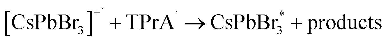
Herein, in view of the importance of the study of interfacial ECL characteristics, a three-phase interface of electrode–emitter–electrolyte has been established by a partially uncovered CsPbBr3 PNC film on a glassy carbon electrode (GCE) surface (Fig. 1). The constructed three-phase interfaces enable the interfacial electrons (or holes) to be effectively injected into the perovskite layer. As illustrated in Fig. 1, the strong reducing intermediate generated from the coreactant, tripropylamine (TPrA), reacts with the strong oxidant of  PNCs, to produce the excited state of CsPbBr3 PNCs and then generate the ECL at the constructed interfaces. Accordingly, the ECL response will be enhanced with the increase of the three-phase interfaces. Moreover, enhanced ECL signal could also be observed on a thicker perovskite film due to the larger area of the exposed three-phase interface since the thickness of the film at the micron level increases with increasing grain boundary, which gives new insights in interface engineering for perovskite films.
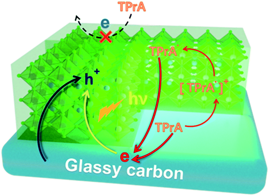 | ||
| Fig. 1 Schematic of ECL reactions on the three-phase interface consisting of glassy carbon, CsPbBr3 PNCs and acetonitrile (containing 10 mM TPrA). | ||
Experimental
Methods
![[thin space (1/6-em)]](https://www.rsc.org/images/entities/char_2009.gif) 000 rpm for 10 min to discard the supernatant, and then the precipitates were washed with hexane two times by centrifugation. Finally, the precipitates were dried in a vacuum drying oven for subsequent use.
000 rpm for 10 min to discard the supernatant, and then the precipitates were washed with hexane two times by centrifugation. Finally, the precipitates were dried in a vacuum drying oven for subsequent use.
Results and discussion
The obtained CsPbBr3 PNCs display a distinct excitonic absorption peak around 504 nm and a sharp photoluminescence (PL) peak at 511 nm with a full width at half-maximum (FWHM) of 18 nm, demonstrating a bright green emission under 365 nm UV light (Fig. 2a). In addition, the CsPbBr3 PNCs present good monodispersity with an average size of 13 nm and could be well dispersed in hexane, which is beneficial for the CsPbBr3 PNC film fabrication. In this study, a CsPbBr3 PNC film was fabricated by drop-coating 5.0 μL of colloidal CsPbBr3 PNC slurry (0.1 g mL−1) on a GCE surface. The film was then left to dry naturally (Fig. 2b) for the subsequent ECL investigation. CsPbBr3 PNCs were dropped on the electrode surface with a high concentration compared with those reported in the literature.6,7,9 In addition, the relatively slow process of solvent evaporation with the appropriate amount of ligands on CsPbBr3 PNCs makes it relatively easier to fabricate a compact film. The scanning electron microscopy (SEM) image shown in Fig. S1a† illustrates that the CsPbBr3 PNC film on the GCE is quite compact with a micron level thickness. The surface roughness of the CsPbBr3 PNC film was further characterized using atomic force microscopy (AFM). As shown in Fig. S2,† the AFM image clearly reveals that the surface roughness is around 2 nm. These results confirm the compact and pin-hole free surface of the CsPbBr3 PNC film (Fig. S2a†), which is quite important for the three-phase interface construction.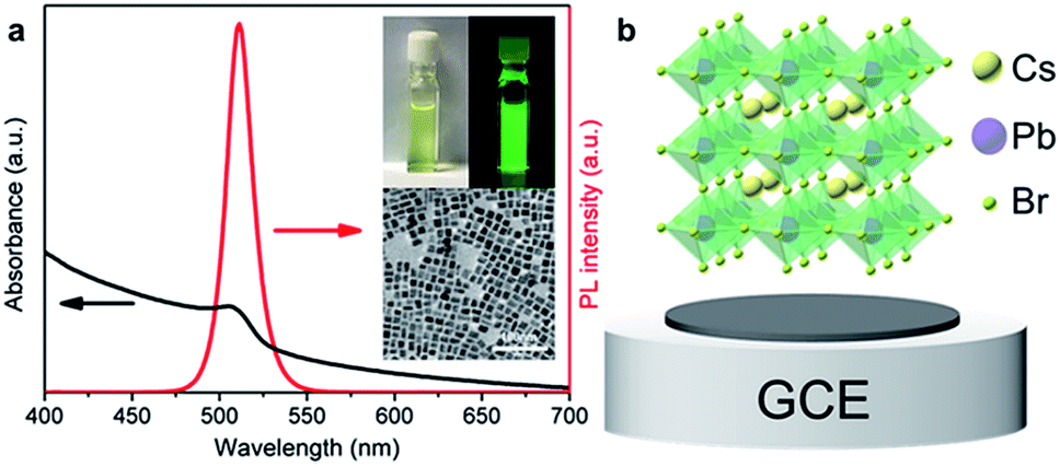 | ||
| Fig. 2 (a) PL (red line) and UV-vis absorption (black line) spectrum of CsPbBr3 PNCs dispersed in hexane. Inset: the upper one shows CsPbBr3 PNCs under visible light (lamp off) and UV light (365 nm, lamp on); the bottom one shows the TEM image of CsPbBr3 PNCs. (b) Schematic diagram of CsPbBr3 PNCs|GCE. | ||
In this study, ECL tests were performed in acetonitrile solution containing 10 mM TPrA. In the ECL process, acetonitrile was introduced as the electrolyte on account of its favorable conductivity and the low solubility of CsPbBr3 PNCs. Owing to the presence of the insulating oleylamine (OAm) ligands on the surface of CsPbBr3 PNCs, electrons are severely blocked in the electrolyte, which impedes electron injection into the CsPbBr3 layer and the GCE is covered with CsPbBr3 PNCs in a compact manner. This point could be confirmed well from the undetectable current and ECL signal using the GCE with a compactly covered film of CsPbBr3 layer (Fig. 3b). A control experiment was conducted in the absence of TPrA (Fig. 3b). There is also no ECL response with the compact film. Surprisingly, the electrolytic current and ECL signal obviously increased when the CsPbBr3 film was partially uncovered by gently scraping the compact film to remove the partial-film (Fig. 3b). In addition, compared with the compactly covered film, the electrochemical impedance spectrum (EIS) reveals obvious impedance decrease when a small amount of the CsPbBr3 film was removed to expose the GCE surface (Fig. 3d). This result indicates that the formation of the interface among CsPbBr3 PNCs, glassy carbon and acetonitrile (containing TPrA) opens up the electron or hole transmission channel, and thus triggers the whole reaction. After the ECL measurement, the CsPbBr3 film remains compact (Fig. S1b†), indicating that the electrolyte has failed to infiltrate into the film and the ECL signal merely generates on the interfaces.
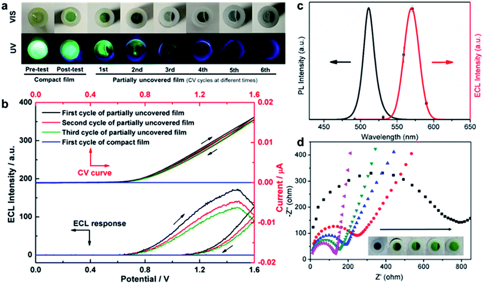 | ||
| Fig. 3 ECL response of CsPbBr3 PNCs|GCE in acetonitrile containing 10 mM TPrA under continuous cycling scans from 0 V to 1.6 V. The scan rate was set at 0.05 V s−1. (a) Pattern changes of CsPbBr3 PNCs|GCE before and after several CV cycles. Top row images were taken under visible light, and bottom row images were taken under 365 nm UV light. (b) The ECL emission and cyclic voltammograms from the compact film and partially uncovered film under cycle scans for one to three cycles, respectively. (c) PL (black line, left) and ECL (red line, right) spectra of CsPbBr3 PNCs|GCE. (d) EIS curve of CsPbBr3 PNCs|GCE with different areas of exposed glassy carbon. | ||
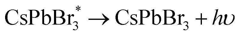
As a classical coreactant, the addition of TPrA significantly enhances the anodic ECL signal. In a specific reaction process, with a continuous positive scan from 0 V to 1.6 V in the presence of TPrA, CsPbBr3 is transformed to a strong oxidizing intermediate [CsPbBr3]+˙ and TPrA is transformed to a strong reducing intermediate, TPrA˙, respectively. TPrA˙ is the electron donor at the three-phase interface, and the partially uncovered glassy carbon interface acts as an electron transmission bridge, which combines with [CsPbBr3]+˙ to generate an excited state  and finally produce the ECL. Without the three-phase interface, electron transmission is blocked, which inhibits ECL generation.
| CsPbBr3 − e− → [CsPbBr3]+˙ |
| TPrA − e− → TPrA˙ + H+ |
The ECL emission peak was found to be 569 nm with a FWHM of 26 nm, showing a red shift of 58 nm compared with the PL emission of CsPbBr3 PNCs (Fig. 3c). Such a red shift illustrates that there is a difference between the ECL and PL processes. In general, ECL performance is closely related to the surface state which may lead to a red shift.33 On one hand, the impact of ligands cannot be ignored as they reflect the surface properties of CsPbBr3 PNCs and influence the electron transfer process. On the other hand, the secondary growth of CsPbBr3 PNCs on the surface leads to an increase in the size of CsPbBr3 PNCs. It changes the surface state of the CsPbBr3 PNCs and causes the ECL red shift. Since the ECL experiments were carried out in acetonitrile and the potential was repeatedly applied, as shown in Fig. 3a, the color of the CsPbBr3 PNC film gradually changed from green-yellow to white with increase in the cycle number in the cyclic voltammetry (CV) measurements. The corresponding ECL responses also show an attenuated tendency (Fig. 3b). Following the verification of the CsPbBr3 film, the frequent re-construction of the surface may cause response attenuation, relative to the dissolution and recrystallization processes because of the low solubility of CsPbBr3 in acetonitrile.
In order to verify the presumption that CsPbBr3 PNCs undergo reconstruction on the electrode surface, SEM images of the CsPbBr3 film before and after ECL measurements were observed. As shown in Fig. 4a–c, a smooth surface could be found for the pristine film, while the bulk crystals at the micron level appeared at the boundary after 5 continuous cycles of the potential scan from 0 V to 1.6 V. The X-ray diffraction (XRD) patterns of the CsPbBr3 films after CV scans show no new diffraction peaks compared with that of the pristine CsPbBr3 film (Fig. 4d). The typical diffraction peaks at 15.3°, 21.7° and 30.7° correspond to the (100), (110) and (200) crystal facets of the cubic CsPbBr3 nanocrystals (PDF#54-752) in these samples, which indicates that the CV process is not related to the phase transformation of CsPbBr3. Therefore, the reconstruction of CsPbBr3 on the surface is only correlated with the change in crystal size. To further prove this observation, the bromine content in the electrolyte after the CV scan was determined using the reported halide exchange strategy.4 In the determination, after the CV scan (5 cycles) the electrolyte was added to the CsPbI3 PNC dispersion (Fig. S4†). Eventually, the PL peak exhibited a significant blue shift, indicating that Br− was indeed partially dissolved in the electrolyte during the ECL reaction. For comparison, the electrode covered by the CsPbBr3 film was soaked in acetonitrile for 5 min without galvanization (the time period is equivalent to the time for CV scan). When pure acetonitrile was directly added to the dispersion solution, a small red shift of the PL peak of CsPbI3 PNCs could be observed since acetonitrile acts as an anti-solvent to agglomerate CsPbI3 PNCs in toluene. In addition, results from the Energy Dispersive Spectrum (EDS) experiment also confirm the loss of bromine (Fig. S5†). With the increase of cycle scan number, the percentage of Br atoms at the three-phase interface decreases continuously. The absence of Br− verifies the regrowth of the layer in the reaction. In addition, the small amount of CsPbI3 PNCs on the electrode surface compared with a relatively large amount of electrolyte also leads to partial ligand dissolution.34 Therefore, obvious aggregation results in secondary growth and micron scale crystals. With continuous CV scanning, the CsPbBr3 PNC film undergoes fragmentation and pore formation gradually. After 10 cycles, plenty of lamellae appearing on the film surface indicate the collapse of the perovskite structure and the continuous decrease of the corresponding ECL response. From the observation of the film structure during the ECL process, it is found that CsPbBr3 PNC films are always subject to the trend of constant remodeling and disintegration. Therefore, it is necessary to adopt bulk perovskites or a thicker film to achieve relatively enduring and stable ECL signals due to the stability of the perovskite in the electrolyte and the resistance to the potential erosion.
 | ||
| Fig. 4 SEM image of CsPbBr3 PNCs|GCE with half area exposure of the electrode surface under cyclic voltammetry scanning steps from 0 to 1.6 V for (a) 0; (b) 5; (c) 10 cycles. Insets show surface conditions around the boundary between the exposed glassy carbon interface and CsPbBr3 PNC film. (d) XRD patterns of CsPbBr3 PNCs subjected to CV cycle steps from 0 to 1.6 V for 0, 5, 10, 15 times, respectively. All scan rates are set at 0.05 V s−1. | ||
In order to investigate the effect of the three-phase interface exposure area on the ECL response, a three-phase interface was fabricated semi-quantitatively by properly uncovering the perovskite film from the same electrode surface (Fig. 5). Different removing patterns for the three-phase interface construction are described in Fig. S6.† The corresponding electrochemical active area (A) could be estimated following the previous report (Table S1†).35 In the process of continuous removal, we found that the ECL response on removing a quarter of the CsPbBr3 PNC film (pattern I) is close to that of half removal (pattern II, Fig. 5a). However, EIS curves, as shown in Fig. S7,† reveal that the impedance decreased obviously with the exposure area increase of the GCE. The electrode conductivity increase means that there are more electrons taking part in the ECL reaction. In fact, whether it is the quarter-removed or the half-removed film (pattern I/pattern II), the effective exposure area of the three-phase interface is almost the same due to the same length of the two radii and the thickness of the layer (5 μL CsPbBr3 PNCs coated). Considering the ECL response in the continuous removal mode (Fig. 5a), it is manifested that the number of electrons involved in the reaction on the three-phase interface is limited. The extra electrons do not participate in the ECL reaction, but cause increase in the conductivity. On the other hand, in the mode of removing at intervals (Fig. 5b and c), ECL response is enhanced for the two quarters-removed film (pattern III) compared with the quarter-removed film (pattern I) as shown in Fig. 5b. Moreover, the exposed area of the two quarters-removed film on the GCE surface (pattern III) is the same as the half-removed film (pattern II) while the effective area of the three-phase interface is different. That is, the former interface involves a length of about four radii and a thickness of one layer. It is thus clear that the ECL response of the perovskite film has no significant relationship with the exposed area of the GCE surface, but is closely related to the effective three-phase interface. Similarly, as shown in Fig. 5c, comparing the three-sixth-removed film (pattern V) by interval removal with the one sixth-removed film (pattern IV) the strength increases by nearly sevenfold, which further reveals the importance of the three-phase interface exposure. In addition, as shown in Fig. S8,† the ECL intensity is in nearly direct proportion to the number of three-phase interfaces which reiterates the interface model for the ECL of CsPbBr3 PNCs.
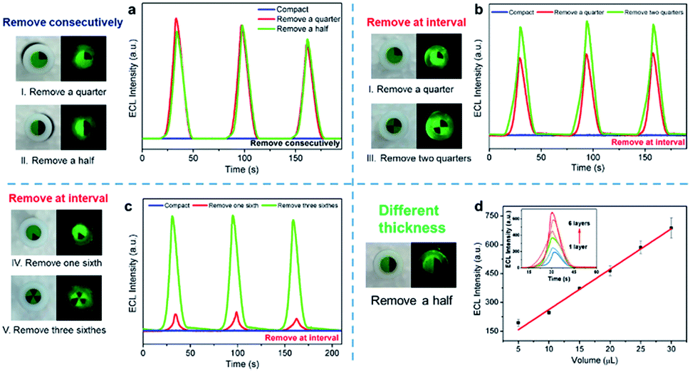 | ||
| Fig. 5 Three-phase interface construction and corresponding ECL response. The interfaces were constructed with two film removal models: (a) consecutive removal; (b and c) removal at intervals. (d) Different thicknesses by multi-layer drop-coating from 1 layer to 6 layers with removing a half of the film. All experiments under continuous cycling scans from 0 to 1.6 V in acetonitrile, the scan rate was 0.05 V s−1. | ||
In addition, the ECL responses show a linear increase trend as the boundary thickness of the CsPbBr3 PNC film prepared by multi-layer drop-coating along with the half-removed film as shown in Fig. 5d. The sectional view of the electrode with different layers is recorded in the SEM images (Fig. S9†). Combined with the interfacial behavior of the ECL reaction as aforementioned, we speculate that the glassy carbon (electrode) injects holes into the CsPbBr3 PNC film and produces sufficient TPrA˙ radicals (coreactant in the electrolyte), thereby the thicker CsPbBr3 PNC film (emitters) produces positive radicals [CsPbBr3]+˙ to accept more electrons from TPrA˙ radicals on the three-phase interface, which ultimately increases the ECL response.
Conclusions
Previous studies on the ECL of perovskites have always focused on electrochemical processes rather than the electrode interfaces. In this study, we revealed the interfacial ECL characteristics of perovskite nanocrystals in acetonitrile, and properly established the relationship between the construction of a three-phase interface and ECL response. We verified that with the increase of three-phase interfaces, that is, the more interfaces meeting with the essential conditions of ECL, stronger ECL signals could be obtained. This work provides a new idea to explore the ECL characteristics of perovskite, presenting a unique angle for interface engineering construction of perovskite film.Conflicts of interest
There are no conflicts to declare.Acknowledgements
This research work is financially supported by the National Natural Science Foundation of China (21876141, 21675133), the Foundation for Innovative Research Groups of the National Natural Science Foundation of China (Grant No. 21521004), and the Shenzhen Science and Technology Project (No. JCYJ20180306172823786).Notes and references
- T. Xuan, J. Huang, H. Liu, S. Lou, L. Cao, W. Gan, R.-S. Liu and J. Wang, Chem. Mater., 2019, 31, 1042–1047 CrossRef CAS.
- Y. Li, X. Wang, W. Xue, W. Wang, W. Zhu and L. Zhao, Nano Res., 2019, 12, 785–789 CrossRef CAS.
- M. V. Kovalenko, L. Protesescu and M. I. Bodnarchuk, Science, 2017, 358, 745–750 CrossRef CAS PubMed.
- Q. A. Akkerman, V. D'Innocenzo, S. Accornero, A. Scarpellini, A. Petrozza, M. Prato and L. Manna, J. Am. Chem. Soc., 2015, 137, 10276–10281 CrossRef CAS PubMed.
- C. Zhou, Y. Tian, O. Khabou, M. Worku, Y. Zhou, J. Hurley, H. Lin and B. Ma, ACS Appl. Mater. Interfaces, 2017, 9, 40446–40451 CrossRef CAS PubMed.
- Y. Huang, M. Fang, G. Zou, B. Zhang and H. Wang, Nanoscale, 2016, 8, 18734–18739 RSC.
- X. Tan, B. Zhang and G. Zou, J. Am. Chem. Soc., 2017, 139, 8772–8776 CrossRef CAS PubMed.
- Y. Cao, Z. Zhang, L. Li, J. R. Zhang and J. J. Zhu, Anal. Chem., 2019, 91, 8607–8614 CrossRef CAS PubMed.
- Y. Huang, X. Long, D. Shen, G. Zou, B. Zhang and H. Wang, Inorg. Chem., 2017, 56, 10135–10138 CrossRef CAS PubMed.
- J. Xue, Z. Zhang, F. Zheng, Q. Xu, J. Xu, G. Zou, L. Li and J. J. Zhu, Anal. Chem., 2017, 89, 8212–8216 CrossRef CAS PubMed.
- L. Li, Z. Zhang, Y. Chen, Q. Xu, J. R. Zhang, Z. Chen, Y. Chen and J. J. Zhu, Adv. Funct. Mater., 2019, 1902533, DOI:10.1002/adfm.201902533.
- Q. Zhai, J. Li and E. Wang, ChemElectroChem, 2017, 4, 1639–1650 CrossRef CAS.
- Z. Cai, F. Li, W. Xu, S. Xia, J. Zeng, S. He and X. Chen, Nano Res., 2018, 11, 1447–1455 CrossRef CAS.
- X. Chen, Y. Liu and Q. Ma, J. Mater. Chem. C, 2018, 6, 942–959 RSC.
- L. Yang, Y. Li, Y. Zhang, D. Fan, X. Pang, Q. Wei and B. Du, ACS Appl. Mater. Interfaces, 2017, 9, 35260–35267 CrossRef CAS PubMed.
- J. Pan, Y. Shang, J. Yin, M. De Bastiani, W. Peng, I. Dursun, L. Sinatra, A. M. El-Zohry, M. N. Hedhili, A. H. Emwas, O. F. Mohammed, Z. Ning and O. M. Bakr, J. Am. Chem. Soc., 2018, 140, 562–565 CrossRef CAS PubMed.
- B. Luo, Y. C. Pu, S. A. Lindley, Y. Yang, L. Lu, Y. Li, X. Li and J. Z. Zhang, Angew. Chem., Int. Ed. Engl., 2016, 55, 8864–8868 CrossRef CAS PubMed.
- D. N. Dirin, S. Dreyfuss, M. I. Bodnarchuk, G. Nedelcu, P. Papagiorgis, G. Itskos and M. V. Kovalenko, J. Am. Chem. Soc., 2014, 136, 6550–6553 CrossRef CAS PubMed.
- C. Zhang, B. Wang, Q. Wan, L. Kong, W. Zheng, Z. Li and L. Li, Nanoscale, 2019, 11, 2602–2607 RSC.
- J. H. Park, A. Y. Lee, J. C. Yu, Y. S. Nam, Y. Choi, J. Park and M. H. Song, ACS Appl. Mater. Interfaces, 2019, 11, 8428–8435 CrossRef CAS PubMed.
- L. Wu, Q. Zhong, D. Yang, M. Chen, H. Hu, Q. Pan, H. Liu, M. Cao, Y. Xu, B. Sun and Q. Zhang, Langmuir, 2017, 33, 12689–12696 CrossRef CAS PubMed.
- J. Zhang, L. Zhang, X. Li, X. Zhu, J. Yu and K. Fan, ACS Sustainable Chem. Eng., 2019, 7, 3487–3495 CrossRef CAS.
- A. Z. Chen, M. Shiu, X. Deng, M. Mahmoud, D. Zhang, B. J. Foley, S.-H. Lee, G. Giri and J. J. Choi, Chem. Mater., 2019, 31, 1336–1343 CrossRef CAS.
- X. Li, D. Yu, J. Chen, Y. Wang, F. Cao, Y. Wei, Y. Wu, L. Wang, Y. Zhu, Z. Sun, J. Ji, Y. Shen, H. Sun and H. Zeng, ACS Nano, 2017, 11, 2015–2023 CrossRef CAS PubMed.
- M. Yuan, L. N. Quan, R. Comin, G. Walters, R. Sabatini, O. Voznyy, S. Hoogland, Y. Zhao, E. M. Beauregard, P. Kanjanaboos, Z. Lu, D. H. Kim and E. H. Sargent, Nat. Nanotechnol., 2016, 11, 872–877 CrossRef CAS PubMed.
- Z. K. Tan, R. S. Moghaddam, M. L. Lai, P. Docampo, R. Higler, F. Deschler, M. Price, A. Sadhanala, L. M. Pazos, D. Credgington, F. Hanusch, T. Bein, H. J. Snaith and R. H. Friend, Nat. Nanotechnol., 2014, 9, 687–692 CrossRef CAS PubMed.
- G. Li, Z. K. Tan, D. Di, M. L. Lai, L. Jiang, J. H. Lim, R. H. Friend and N. C. Greenham, Nano Lett., 2015, 15, 2640–2644 CrossRef CAS PubMed.
- J. Wang, N. Wang, Y. Jin, J. Si, Z. K. Tan, H. Du, L. Cheng, X. Dai, S. Bai, H. He, Z. Ye, M. L. Lai, R. H. Friend and W. Huang, Adv. Mater., 2015, 27, 2311–2316 CrossRef CAS PubMed.
- R. Long, J. Liu and O. V. Prezhdo, J. Am. Chem. Soc., 2016, 138, 3884–3890 CrossRef CAS PubMed.
- M. Yang, Y. Zeng, Z. Li, D. H. Kim, C. S. Jiang, J. van de Lagemaat and K. Zhu, Phys. Chem. Chem. Phys., 2017, 19, 5043–5050 RSC.
- B. Li, J. Tian, L. Guo, C. Fei, T. Shen, X. Qu and G. Cao, ACS Appl. Mater. Interfaces, 2016, 8, 4684–4690 CrossRef CAS PubMed.
- F. Lin, F. Li, Z. Lai, Z. Cai, Y. Wang, O. S. Wolfbeis and X. Chen, ACS Appl. Mater. Interfaces, 2018, 10, 23335–23343 CrossRef CAS PubMed.
- Z. Ding, B. M. Quinn, S. K. Haram, L. E. Pell, B. A. Korgel and A. J. Bard, Science, 2002, 296, 1293–1297 CrossRef CAS PubMed.
- X. Li, D. Yu, F. Cao, Y. Gu, Y. Wei, Y. Wu, J. Song and H. Zeng, Adv. Funct. Mater., 2016, 26, 5903–5912 CrossRef CAS.
- P. Podesva, I. Gablech and P. Neuzil, Anal. Chem., 2018, 90, 1161–1167 CrossRef CAS PubMed.
Footnotes |
| † Electronic supplementary information (ESI) available. See DOI: 10.1039/c9na00456d |
| ‡ These authors contributed equally. |
| This journal is © The Royal Society of Chemistry 2019 |