
 Open Access Article
 This Open Access Article is licensed under a Creative Commons Attribution-Non Commercial 3.0 Unported Licence
AC parallel local oxidation of silicon
Zahra
Hemmatian†‡
a,
Denis
Gentili†
 a,
Marianna
Barbalinardo
a,
Vittorio
Morandi
b,
Luca
Ortolani
b,
Giampiero
Ruani
a and
Massimiliano
Cavallini
*a
a,
Marianna
Barbalinardo
a,
Vittorio
Morandi
b,
Luca
Ortolani
b,
Giampiero
Ruani
a and
Massimiliano
Cavallini
*a
aIstituto per lo Studio dei Materiali Nanostrutturati, Consiglio Nazionale delle Ricerche, Via P. Gobetti 101, 40129 Bologna, Italy. E-mail: massimilliano.cavallini@cnr.it
bIstituto per la Microelettronica e i Microsistemi, Consiglio Nazionale delle Ricerche, Via P. Gobetti 101, 40129 Bologna, Italy
First published on 3rd September 2019
Abstract
Here, we present a suitable advancement of parallel local oxidation nanolithography, demonstrating its feasibility in alternate current mode (AC-PLON). For demonstration, we fabricated model structures consisting of an array of parallel nanostripes of electrochemical SiOx with a controlled roughness. Besides, we proved the repeatability of AC-PLON and its integrability with conventional parallel local oxidation nanolithography.
Since the commercialisation of atomic force microscopy (AFM), local anodic oxidation, also named as oxidative scanning probe lithography (O-SPL), has been studied for an impressive variety of applications, mostly related to the local oxidation of silicon. The key factors of its success are the simplicity of the technique, the availability of instrumentation (most of the commercial instruments are implemented by SPL), its versatility and its compatibility with ambient conditions without the need for specialized infrastructures, such as clean rooms. O-SPL has been applied for nanopatterning, to fabricate barriers, masks and devices; moreover, acting on the bias sign, it has been used to perform electrochemical reduction and nanochemistry. Several authoritative reviews and books report on the O-SPL mechanism and its applications.1–4
Although O-SPL has many advantages for proof-of-concept at the laboratory scale, it exhibits the typical drawbacks of lithography based on scanning probe microscopy: i.e. limited throughput due to its serial nature (the structures are fabricated one by one) and a practical patternable area that is limited to the maximum scan size of the piezoelectric scanner (usually a few hundred microns range). These limits have been addressed by using an array of cantilevers5 or, more efficiently, using parallel local oxidation nanolithography (PLON) in which the AFM tip is replaced by the protrusions of a conductive stamp.6–9
Although the final result of PLON is the same as that of O-SPL, i.e. Si oxidation, the two methods proceed with a different mechanism; this is due to the different shape and radius of the stamp protrusions with respect to the AFM tips (>300 nm in PLON and ∼10 nm in O-SPL). These differences act on some important parameters of the printed structures, such as the thickness (in PLON they are one order of magnitude thicker than in O-SPL) and the mechanical properties. The details of PLON are discussed in ref. 8.
PLON has been proved to work on a large scale (up to 1 × 1 cm2) with <100 nm resolution;6 it has been successfully used for silicon oxidation,6,8 constructive lithography,10 template growth of molecules,11 splitting of CO2,12 embedding of magnetic nanoparticles13 and fabrication of self-regenerating resistive switch devices,14 and more recently to fabricate large area patterns of nanodots of manganite in a local reduction configuration.15 To date, PLON has only been demonstrated applying a DC voltage. Here, we present an advancement of PLON demonstrating its application in AC mode for the fabrication of precise nanostructures of electrochemical SiOx (e-SiOx) with a controlled roughness. As a model structure, we printed an ordered array of stripes ca. 100 nm wide, a kind of pattern usually used for the demonstration of fabrication techniques and used for a variety of applications.16,17
The PLON process has been performed on p-doped silicon substrates, using the conventional set-up for PLON,8 schematized in Fig. 1 and detailed in ref. 8.
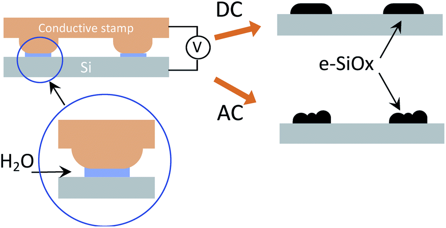 | ||
| Fig. 1 Scheme of parallel local oxidation nanolithography (PLON) applied on silicon. Applying a DC voltage with Si at the positive pole (DC-PLON) produces e-SiOx nanostructures replicating the stamp protrusions; using AC bias (AC-PLON), it produces a pattern of nano-grains. | ||
In PLON a conductive stamp is placed in contact with the surface in a highly humid environment (RH > 80%). In this condition, a water bridge forms between the stamp protrusions and the surface forming an array of two-electrode electrochemical nanocells (Fig. 1).
By applying a bias, the sample surface is oxidized or electrochemically reduced. This process takes place only under the stamp protrusions, whose size defines the spatial resolution of the technique. The use of an electrochemically inert stamp (i.e. a polymer coated by a thin film of gold) prevents its degradation due to redox reactions.
As occurs using scanning probe tips,18,19 AC-PLON is more efficient than DC-PLON; in fact, in AC mode the process occurs applying a bias voltage higher than 6 V, while operating in DC mode, the same set-up requires a bias higher than 15 V.6
Applying a bias voltage below 6 V, the patterns fabricated by AC-PLON are not homogeneous and poorly reproducible. At the end of the process no current flow is observed between the conductive stamp and the substrate, indicating that the printed features produced by AC-PLON are insulating.
Fig. 2 shows a morphology characterization of parallel stripes obtained by AC-PLON applying 8 V bias for 60 s (50 Hz) and the corresponding pattern obtained by DC-PLON applying 30 V for 60 s (these parameters were chosen in order to fabricate nano-stripes with comparable size).
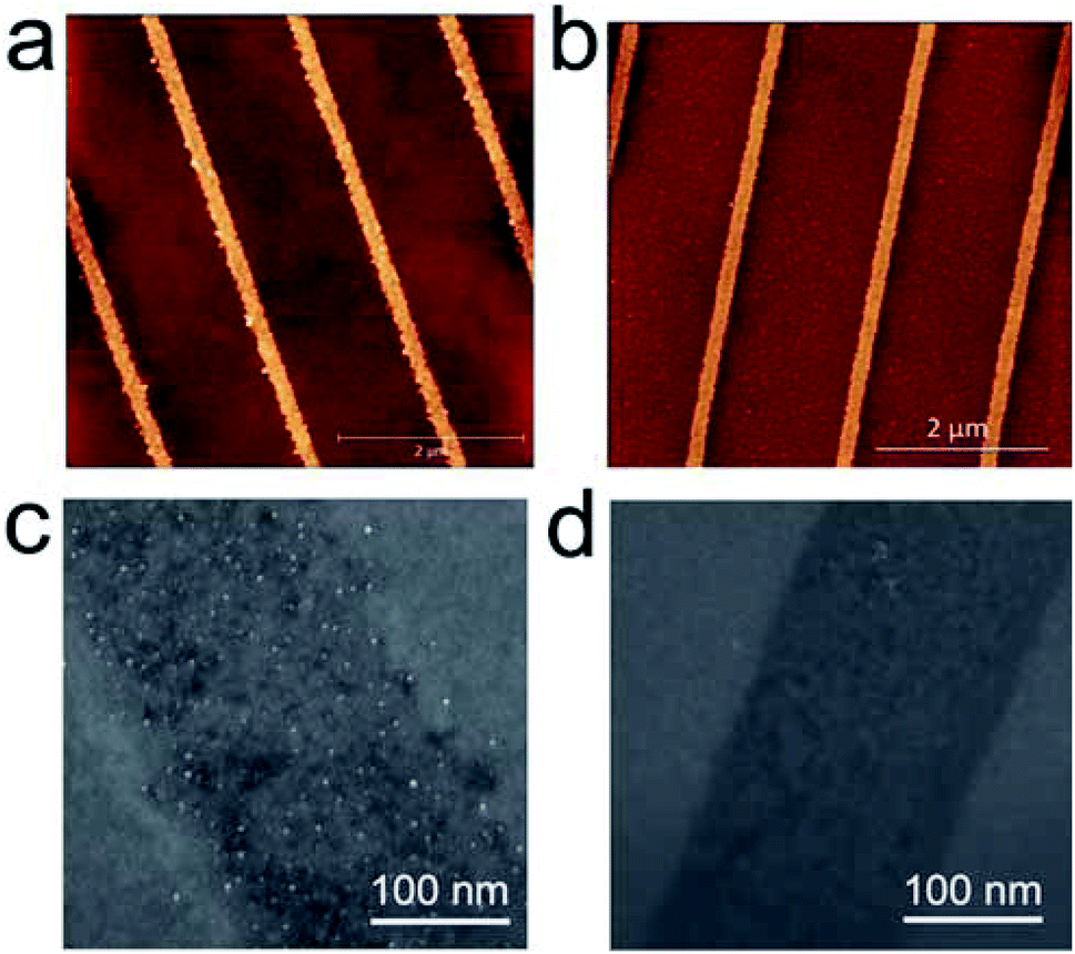 | ||
| Fig. 2 Morphological characterization of freshly prepared e-SiOx nanostripes, fabricated by PLON in DC and AC mode. (a) AFM topography of stripes printed in AC mode. Z scale is 0–8 nm. (b) AFM topography of stripes printed in DC mode. Z scale is 0–8 nm. Secondary electron SEM micrographs of stripes printed in (c) AC mode and (d) DC mode. | ||
Although the nanostripes fabricated in DC mode need higher voltage and longer time, the stripes built in AC mode mainly exhibit a higher roughness (<1.0 nm vs. >2.0 nm). A morphological investigation performed by AFM and SEM shows that the higher roughness is due to the formation of grains inside the electrochemical SiOx stripes fabricated using AC-PLON. The grains appear homogeneously distributed inside the printed stripes, and no sign of order or spatial correlation was observed among them, when printing stripes in the width range of 100–700 nm.
Noticeably, both the stripe thickness and grain size are almost independent of the applied AC voltage and the time of bias application (Fig. 3).
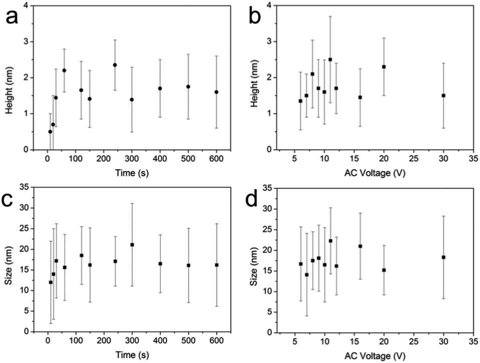 | ||
| Fig. 3 Effect of time of oxidation and voltage on the height and size diameter of grains fabricated by AC-PLON. (a) Time evolution of grain height; voltage 10 V. (b) Effect of bias voltage on the grain height; oxidation time 300 s. (c) Time evolution of grain size; voltage 10 V. (d) Bias voltage effect on the grain size; ox. time 300 s.3 | ||
In order to demonstrate the versatility and the repeatability of the PLON, we fabricated a more complex pattern of e-SiOx. The pattern was obtained by applying PLON in a two-step process, i.e. first we fabricated a pattern of parallel stripes with low roughness applying AC-PLON in one direction, and then we repeated the process applying DC-PLON after a 90° rotation of the stamp. Fig. 4 shows the AFM morphology of the printed pattern, which clearly shows a different roughness.
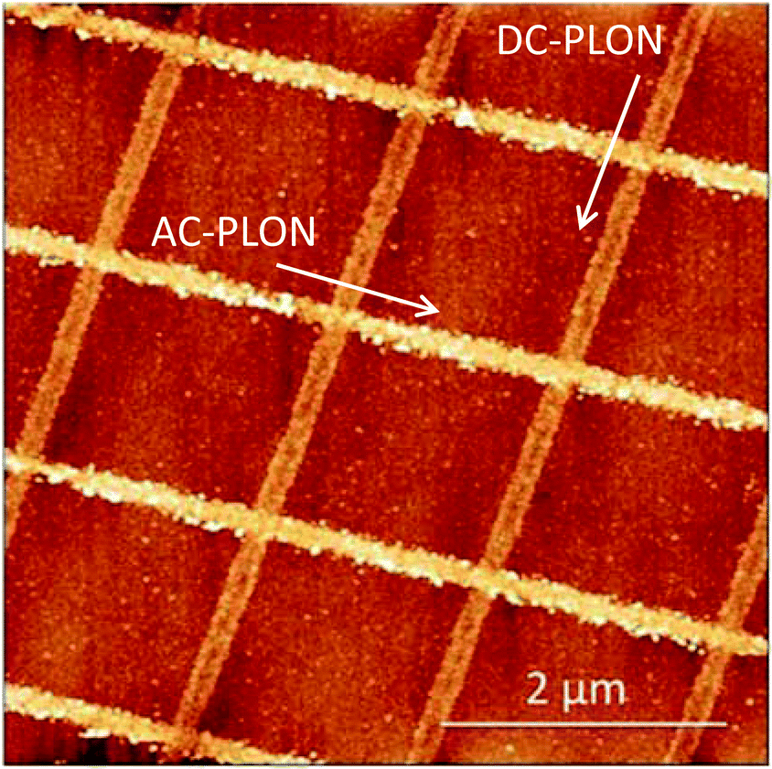 | ||
| Fig. 4 AFM morphology of the complex pattern obtained by the application of DC- and AC-PLON along perpendicular directions. | ||
The nature of the grain's formation by AC-PLON was investigated by AFM, SEM, XPS and μ-Raman spectroscopy.
SEM microanalysis and XPS (data not shown) do not show any traces of metal contaminants in the samples prepared by AC-PLON. This evidence allows us to exclude the presence of contaminants deposited from the stamp as the origin of grain formation. On the other hand, important information was obtained from μ-Raman spectroscopy, which has been recognized as an efficient technique to characterize silicon nanostructures.20
Fig. 5 shows the spectra of freshly prepared samples (i.e. within a few hours from preparation) fabricated in DC and AC mode, respectively. While the spectrum of the nanostripes fabricated by DC-PLON shows only the characteristic transversal optic mode (TO) peak of crystalline silicon (c-Si) at 520 cm−1, the spectrum of the sample fabricated by AC-PLON shows also a quite intense peak at 479 cm−1. The peak at 479 cm−1 is relatively narrow (8 cm−1, only almost twice that of the main Raman peak of c-Si), suggesting that the crystalline domains of these structures are not smaller than a couple of nanometres.
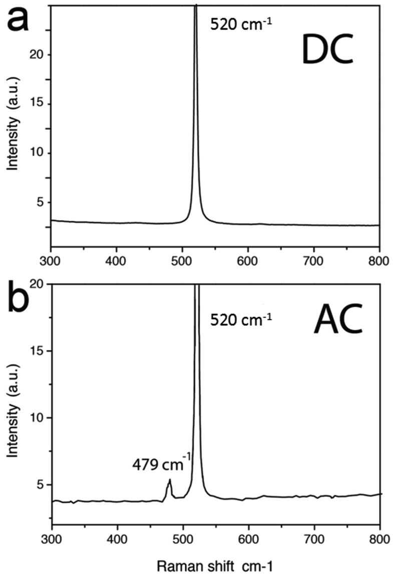 | ||
| Fig. 5 Raman spectra of e-SiOx stripes fabricated by (a) DC-PLON and (b) AC-PLON. The spectrum of e-SiOx stripes printed in DC mode shows only the typical sharp peak at 520 cm−1 of the crystalline Si substrate, while the spectrum of e-SiOx stripes printed in AC mode shows a quite intense peak at 470 cm−1 that can be related to Si nanoclusters. | ||
As a consequence, the energy shift (31 cm−1) of the Raman scattering from the TO mode of c-Si could not be associated only to a phonon confinement model, but possibly to the formation of silicon nanoclusters20,21 or nanoribbons.22 This peak is clearly visible in freshly prepared samples, but disappears after a few hours from sample preparation.
Although we do not have an exhaustive model for grain formation using AC-PLON, we proposed a possible mechanism to explain the grain formation and the evolution of the Raman spectra based on our experimental results and the effect of break-down observed in similar systems applying a large negative bias.
The most important indication is provided by the Raman evidence of the formation of unstable species, probably Si nanoclusters (NCs), upon the application of AC bias. The silicon substrate can be oxidised only during the application of positive bias. It is known that this process can produce metastable species, i.e. not fully oxidised species of Si, such as Si(I) and Si(III).26 We hypothesised that during the phase of application of negative bias, these not fully oxidised Si species are electrochemically reduced forming Si NCs inside the e-SiOx matrix. Noticeably, the formation of Si NCs in the SiO2 matrix was proved by HR-TEM in metal–SiO2–metal junctions, as a consequence of the application of a large negative bias and the break-down of the insulating layer.14,23–25 These conditions are comparable with the experimental condition that we used in AC-PLON. At this stage, the nanoclusters can be detected both by Raman spectroscopy and by SEM since they are partially protected by the SiO2 matrix. Upon the exposition to ambient conditions, Si NCs are spontaneously oxidised within a few hours, as observed by Raman spectrum evolution, generating the stable grains of SiO2.
The evidence that the grain size is not influenced by the size of the printed stripes and the time of oxidation, suggests that the process proceeds by the formation of a defined density of nuclei at the beginning of the process (maybe within the first few seconds). Dedicated investigation of the mechanism of grain formation is ongoing.
Conclusions
In conclusion, we showed an advancement of PLON in which electrochemical reaction is exploited to control the morphology and the spatial distribution of grains in printed stripes, whose positioning can be controlled with the spatial resolution of electrochemical nanolithography. The proposed method is simple, versatile and allows the “fabrication” of nanoclusters and positioning in a single step, with nanometric spatial resolution. Compared to the conventional methods based on scanning probe microscopy, our process is more efficient and works at large area, thus providing clear technological advantages in terms of flexibility and cost. Here, we fabricated SiOx grains inside 100 nm wide stripes, but in principle the same process can be pushed to the limit of resolution of scanning probe lithography (i.e. <10 nm). The parallel nature, the low cost for application and the compatibility with the current silicon technology, indicate that PLON is a possible candidate for industrial implementation as a mid-term application.Experimental
The stamp was made of polydimethylsiloxane (PDMS, Sylgard 184 Down Corning), and it was fabricated by replica moulding of a commercial compact disk.27 The curing process was carried out for 1 hour at 70 °C. Once cured, the replica was peeled off from the master and washed in pure ethanol to remove uncured polymer. After that, the PDMS replica was coated with a 100 nm thick film of metal by thermo joule evaporation. The stamp motif consists of parallel lines with a periodicity of 1.4 μm, width at the apex of 100 nm and depth of 220 nm. A detailed protocol of stamp fabrication is described in ref. 28.The substrates consisted of a 1 × 1 cm2 piece of p-doped Si, covered with a native silicon oxide layer (Siltronic, type n and p, 0.5 mm thick, orientation [100], resistivity 10 < ρ < 20 Ω cm); before PLON they were cleaned by sonication for 2 min in electronic-grade water (Milli-pure quality), 2 min in acetone (Aldrich chromatography quality) and then 2 min in 2-propanol (Aldrich spectroscopic grade quality), and eventually lifted-off using boiling acetone. The substrate and conductive stamps were connected electrically to the potential source (ELIND model 3232). The system was inserted inside a sealed chamber, in which the relative humidity (RH) was controlled by fluxing moist nitrogen. When the RH reached 90%, the stamp and substrate were put mechanically in contact. Then, a bias voltage with limited current (typically 200 mA) was applied between the stamp and surfaces for 60 seconds.
SEM images were obtained with a ZEISS 1530 SEM equipped with a Schottky emitter and operating at 10 keV equipped with an InLens (IL) detector and an Everhart–Thornley detector (ETD) for secondary electron collection. The images reported in the manuscript have been acquired with ETD, showing at the same time morphological as well as compositional/density variations.
All the AFM images were recorded with a standalone AFM (SMENA NT-MDT Moscow) operating in air, in intermittent contact mode at room temperature with a relative humidity of 55%. Si cantilevers (NT-MDT NSG10, with a typical curvature radius of the tip of 10 nm and a typical resonant frequency of 255 kHz) were used. The topographic images were corrected line-by-line for background trend effects by removal of the second-order polynomial fitting.
The Nd-YAG excitation wavelength (532 nm) was used to obtain Raman spectra. Raman scattering measurements were recorded in backscattering configuration using a long working-distance 50× microscope objective with a laser of 15 mW.
Conflicts of interest
There are no conflicts to declare.Acknowledgements
This work was partially supported by the National project PRIN 2017YH9MRK “Novel Multilayered and Micro-Machined Electrode Nano-Architectures for Electrocatalytic Applications”.References
- H. Liu, S. Hoeppener and U. S. Schubert, Adv. Eng. Mater., 2016, 18, 890–902 CrossRef CAS.
- Y. K. Ryu and R. Garcia, Nanotechnology, 2017, 28, 142003 CrossRef PubMed.
- R. Garcia, A. W. Knoll and E. Riedo, Nat. Nanotechnol., 2014, 9, 577–587 CrossRef CAS PubMed.
- F. C. Simeone, C. Albonetti and M. Cavallini, J. Phys. Chem. C, 2009, 113, 18987–18994 CrossRef CAS.
- S. C. Minne, J. D. Adams, G. Yaralioglu, S. R. Manalis, A. Atalar and C. F. Quate, Appl. Phys. Lett., 1998, 73, 1742–1744 CrossRef CAS.
- M. Cavallini, P. Mei, F. Biscarini and R. Garcia, Appl. Phys. Lett., 2003, 83, 5286–5288 CrossRef CAS.
- T. Mühl, J. Kretz, I. Mönch, C. M. Schneider, H. Brückl and G. Reiss, Appl. Phys. Lett., 2000, 76, 786–788 CrossRef.
- C. Albonetti, J. Martinez, N. S. Losilla, P. Greco, M. Cavallini, F. Borgatti, M. Montecchi, L. Pasquali, R. Garcia and F. Biscarini, Nanotechnology, 2008, 19, 435303 CrossRef PubMed.
- J. Martinez, N. S. Losilla, F. Biscarini, G. Schmidt, T. Borzenko, L. W. Molenkamp and R. Garcia, Rev. Sci. Instrum., 2006, 77, 086106 CrossRef.
- R. Maoz, E. Frydman, S. R. Cohen and J. Sagiv, Adv. Mater., 2000, 12, 424–429 CrossRef CAS.
- R. V. Martinez, N. S. Losilla, J. Martinez, M. Tello and R. Garcia, Nanotechnology, 2007, 18, 084021 CrossRef.
- M. Calvaresi, R. V. Martinez, N. S. Losilla, J. Martinez, R. Garcia and F. Zerbetto, J. Phys. Chem. Lett., 2010, 1, 3256–3260 CrossRef CAS.
- M. Cavallini, F. C. Simeone, F. Borgatti, C. Albonetti, V. Morandi, C. Sangregorio, C. Innocenti, F. Pineider, E. Annese, G. Panaccione and L. Pasquali, Nanoscale, 2010, 2, 2069–2072 RSC.
- M. Cavallini, Z. Hemmatian, A. Riminucci, M. Prezioso, V. Morandi and M. Murgia, Adv. Mater., 2012, 24, 1197–1201 CrossRef CAS PubMed.
- M. Cavallini, P. Graziosi, M. Calbucci, D. Gentili, R. Cecchini, M. Barbalinardo, I. Bergenti, A. Riminucci and V. Dediu, Sci. Rep., 2014, 4, 7397 CrossRef CAS PubMed.
- M. Cavallini, A. Calo, P. Stoliar, J. C. Kengne, S. Martins, F. C. Matacotta, F. Quist, G. Gbabode, N. Dumont, Y. H. Geerts and F. Biscarini, Adv. Mater., 2009, 21, 4688–4691 CrossRef CAS.
- A. D. Ruigomez, D. Rodriguez-San-Miguel, K. C. Stylianou, M. Cavallini, D. Gentili, F. Liscio, S. Milita, O. M. Roscioni, M. L. Ruiz-Gonzalez, C. Carbonell, D. Maspoch, R. Mas-Balleste, J. L. Segura and F. Zamora, Chem.–Eur. J., 2015, 21, 10666–10670 CrossRef PubMed.
- M. Calleja, J. Anguita, R. Garcia, K. Birkelund, F. Perez-Murano and J. A. Dagata, Nanotechnology, 1999, 10, 34–38 CrossRef CAS.
- J. A. Dagata, T. Inoue, J. Itoh and H. Yokoyama, Appl. Phys. Lett., 1998, 73, 271–273 CrossRef CAS.
- H. Richter, Z. P. Wang and L. Ley, Solid State Commun., 1981, 39, 625–629 CrossRef CAS.
- R. D. Tilley, J. H. Warner, K. Yamamoto, I. Matsui and H. Fujimori, Chem. Commun., 2005, 1833–1835, 10.1039/b416069j.
- J. Y. Yu, J. Gao, F. H. Xue, X. H. Yu, H. T. Yu, X. L. Dong, H. Huang, A. Ding, X. Quan and G. Z. Cao, RSC Adv., 2015, 5, 68714–68721 RSC.
- J. Yao, Z. Z. Sun, L. Zhong, D. Natelson and J. M. Tour, Nano Lett., 2010, 10, 4105–4110 CrossRef CAS PubMed.
- J. Yao, L. Zhong, D. Natelson and J. M. Tours, J. Am. Chem. Soc., 2010, 133, 941–948 CrossRef PubMed.
- J. Yao, L. Zhong, D. Natelson and J. M. Tour, Sci. Rep., 2012, 2, 242 CrossRef PubMed.
- E. Y. J. Chabal, Fundamental Aspects of Silicon Oxidation, Springer-Verlag, 2001 Search PubMed.
- M. Cavallini, R. Lazzaroni, R. Zamboni, F. Biscarini, D. Timpel, F. Zerbetto, G. J. Clarkson and D. A. Leigh, J. Phys. Chem. B, 2001, 105, 10826–10830 CrossRef CAS.
- M. Melucci, M. Zambianchi, L. Favaretto, V. Palermo, E. Treossi, M. Montalti, S. Bonacchi and M. Cavallini, Chem. Commun., 2011, 47, 1689–1691 RSC.
Footnotes |
| † These authors contributed equally to the present work. |
| ‡ Present address: Department of Electrical Engineering, University of California Santa Cruz, Santa Cruz, CA, 95064, USA. |
| This journal is © The Royal Society of Chemistry 2019 |