
 Open Access Article
 This Open Access Article is licensed under a Creative Commons Attribution-Non Commercial 3.0 Unported Licence
Impact of the Ga flux incidence angle on the growth kinetics of self-assisted GaAs nanowires on Si(111)†
Marco
Vettori
,
Alexandre
Danescu
 *,
Xin
Guan‡
,
Philippe
Regreny
,
José
Penuelas
and
Michel
Gendry
*,
Xin
Guan‡
,
Philippe
Regreny
,
José
Penuelas
and
Michel
Gendry
Université de Lyon, Institut des Nanotechnologies de Lyon – INL, Ecole Centrale de Lyon, UMR CNRS 5270, 69134 Ecully, France. E-mail: alexandre.danescu@ec-lyon.fr
First published on 7th October 2019
Abstract
In this work we show that the incidence angle of group-III element fluxes plays a significant role in the diffusion-controlled growth of III–V nanowires (NWs) by molecular beam epitaxy (MBE). We present a thorough experimental study on the self-assisted growth of GaAs NWs by using a MBE reactor equipped with two Ga cells located at different incidence angles with respect to the surface normal of the substrate, so as to ascertain the impact of such a parameter on the NW growth kinetics. The as-obtained results show a dramatic influence of the Ga flux incidence angle on the NW length and diameter, as well as on the shape and size of the Ga droplets acting as catalysts. In order to interpret the results we developed a semi-empirical analytical model inspired by those already developed for MBE-grown Au-catalyzed GaAs NWs. Numerical simulations performed with the model allow us to reproduce thoroughly the experimental results (in terms of NW length and diameter and of droplet size and wetting angle), putting in evidence that under formally the same experimental conditions the incidence angle of the Ga flux is a key parameter which can drastically affect the growth kinetics of the NWs grown by MBE.
1 Introduction
GaAs nanowires (NWs) are one of the most promising materials for the integration of III–V semiconductors on Si, since they can be grown by molecular beam epitaxy (MBE) on Si substrates via a self-assisted vapor–liquid–solid (VLS) mechanism1–8 preventing the use of Au catalysts which would jeopardize the electronic and optoelectronic properties of these semiconductors, forming deep-level states in both of them.9–14 When it comes to MBE, both Au-catalyzed and self-assisted growths of NWs are diffusion-controlled processes. Many theoretical and experimental studies were carried out to understand the growth mechanisms and to identify the parameters influencing the NW structure and the growth kinetics.2,3,7,15–31 First studies have shown that the catalyst droplet volume or shape15,16,18,27,31 and, more recently, that the droplet wetting angle20,22,24 do control the NW crystal structure through the location of the nucleation site. Moreover, the volume of the catalyst droplet controls the kinetics of the axial growth through the related capture surface,25,26,28 and in particular, through the capture area for As in the case of self-assisted GaAs NWs.18,22Concerning growth parameters, little experimental work has been devoted to the influence of the Ga flux incidence angle on the NW properties. The morphology and chronology of formation of GaN NWs and GaN-AlN core–shell NWs, including the effect of the III and V source positions, were experimentally studied using the AlN marker method in ref. 32 and 33. Regarding the NW growth kinetics, the growth models developed so far take into account the Ga flux incidence angle17,18,22,23,25,26,28,30 but do not demonstrate its influence. As an example, the model of Glas et al.17 for self-assisted GaAs NWs was based on the assumption that the Ga flux adopted is always high enough to supply the Ga droplet, therefore neglecting to consider the influence of the incidence angle of the Ga flux on the amount of Ga atoms collected by the droplets, and consequently on their volume and shape. Thus, despite all these important studies, to the best of our knowledge, no experimental study has been so far undertaken to ascertain how different Ga flux incidence angles can affect the NW growth kinetics under formally the same growth conditions.
Considering that for self-assisted GaAs NWs (i) the Ga droplet volume is determined by the balance between the droplet supply in Ga atoms and its depletion caused by the NW growth, and (ii) the droplet supply in Ga atoms occurs through three different ways, i.e. diffusion of Ga adatoms on the substrate, diffusion of Ga adatoms on the NW facets and direct impingement of Ga atoms on the droplet, it is thus expected that the incidence angle of the Ga flux has an influence on the amount of Ga atoms which can be collected by the droplet.
Based on these considerations, we decided to demonstrate experimentally the influence of the Ga flux incidence angle, further denoted as α, with respect to the surface normal of the substrate (i.e. with respect to the growth axis of vertically grown NWs on the substrate). To this end we used a MBE reactor equipped with two Ga cells at α ≃ 27.9° and α ≃ 9.3° denoted as Ga(5) and Ga(7), respectively. We studied the axial and radial growth rate of GaAs NWs with a series of GaAs NWs grown for different growth times using either the Ga(5) or the Ga(7) cell. The experimental results have been explained by using a semi-empirical model so as to determine the physical factors which originate the significant differences observed with the two different Ga sources.
2 Experimental results
We grew a series of Ga(5)As and Ga(7)As NWs for different growth times ranging from 5 to 80 min, so as to obtain a vast description of the axial growth rate depending on the Ga source used. The growth conditions adopted (cf. – Experimental section) are the same as those employed in ref. 34, which have proved to provide GaAs NWs with zinc-blende (ZB) structure when using the Ga(5) cell.The impact of the incidence angle α on the NW growth kinetics is highlighted in Fig. 1(a) and (b) reporting respectively the evolutions of the NW length and NW diameter (measured at the NW top just below the Ga droplet), as a function of the growth time. SEM images of the as-obtained NWs are shown in Fig. 1 in the ESI.† Firstly, Fig. 1 shows that, as expected, despite the equal value of the Ga(5) and Ga(7) fluxes in terms of planar growth rate (0.5 ML s−1), the α angle exerts a significant influence on the NW growth kinetics. It can be observed that for shorter growth times, the lengths of NWs obtained with Ga(5) and Ga(7) cells are comparable, whereas for longer growth times the Ga(7)As NWs are significantly shorter than their Ga(5)As counterpart. From Fig. 1(a), it can also be noticed that while the experimental points for Ga(5)As NWs can be fitted with a single linear regression corresponding to a NW axial growth rate of 1.9 nm s−1, those ones for Ga(7)As NWs lay on the same slope for growth times up to ≃17 min, but are fitted with a different one for longer growth times, corresponding to a NW axial growth rate of ≃0.8 nm s−1 only. Such a result suggests that in the latter case the growth process undergoes two different growth regimes, named R1 and R2 in Fig. 1(a), with a transition from R1 to R2 at a growth time of about 17 min and corresponding to a NW length of about 1.8 μm (cf. vertical and horizontal dashed blue lines in Fig. 1(a)). As clearly highlighted in Fig. 1(b), the angle α affects not only the NW length evolution with the growth time but also the NW diameter evolution. In particular, while for Ga(5)As NWs the diameter increases linearly with the growth time (≃1 nm min−1), it seems roughly constant (slope ≃ 0.2 nm min−1) in the case of Ga(7)As NWs.
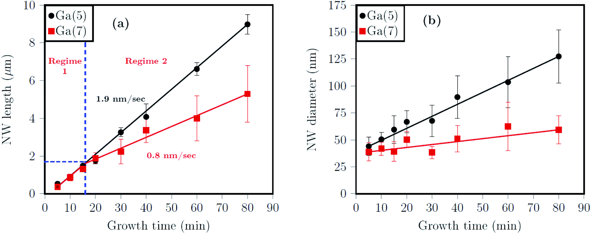 | ||
| Fig. 1 (a) Length of Ga(5)As NWs (black) and Ga(7)As NWs (red) as a function of the growth time. The vertical dashed blue line marks the separation between the two growth regimes observed for Ga(7)As NWs, while the horizontal one shows the corresponding NW length. (b) Diameter of Ga(5)As NWs (black) and Ga(7)As NWs (red) as a function of the growth time. The NW length and diameter are measured on about 100 NWs. | ||
Secondly, a difference in the droplet shape can be observed as the growth time increases (Fig. 2). In fact, while for shorter growth times the Ga droplets present equivalent features and wetting angle β in the 138–142° range for both Ga(5)As and Ga(7)As NWs (Fig. 2(a) and (b)), for longer growth times the droplets exposed to Ga(7) flux present a smaller wetting angle in the 120–130° range (cf.Fig. 2(d) and (f)) than their Ga(5) counterpart (still in the 138–142° range as shown in Fig. 2(c) and (e)). Note that the wetting angle β is calculated from the relation RNW = Rd![[thin space (1/6-em)]](https://www.rsc.org/images/entities/char_2009.gif) sinβ with RNW and Rd being the NW and droplet radii, respectively. It can be stated that the droplets on Ga(7)As NWs, contrary to their Ga(5)As counterparts, tend to decrease in size as the growth time increases. It should also be noticed that the difference in wetting angles between Ga(5) and Ga(7) droplets can affect the crystal structure of the NWs, the former case leading to the ZB structure and the latter one to the wurtzite (Wz) one (cf. Fig. 2 in the ESI†).
sinβ with RNW and Rd being the NW and droplet radii, respectively. It can be stated that the droplets on Ga(7)As NWs, contrary to their Ga(5)As counterparts, tend to decrease in size as the growth time increases. It should also be noticed that the difference in wetting angles between Ga(5) and Ga(7) droplets can affect the crystal structure of the NWs, the former case leading to the ZB structure and the latter one to the wurtzite (Wz) one (cf. Fig. 2 in the ESI†).
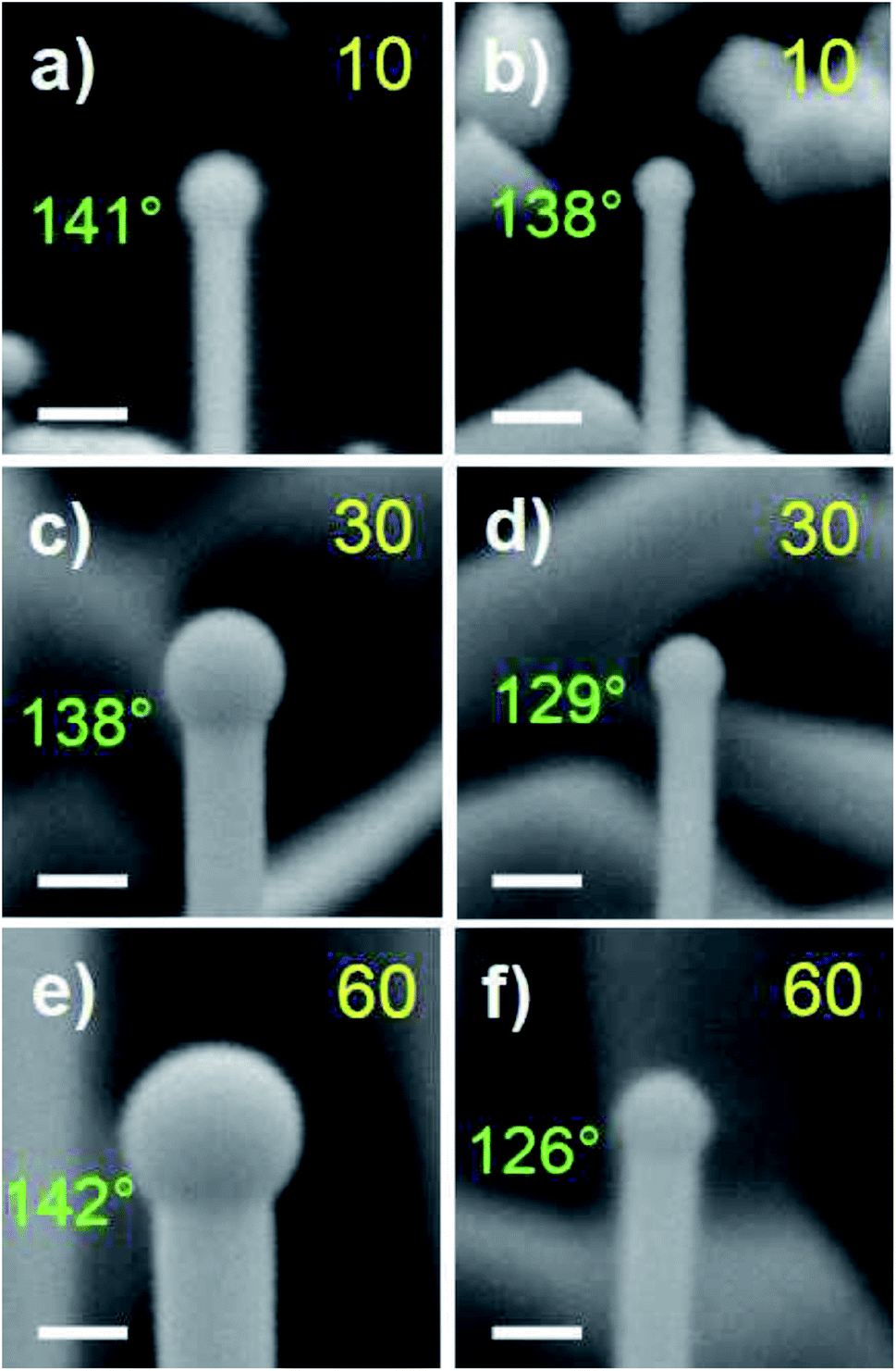 | ||
| Fig. 2 SEM images (45°-tilted) showing the evolution of the Ga droplets at the top of Ga(5)As NWs (left) and Ga(7)As NWs (right) with increasing growth time. The growth time in minutes is indicated by yellow numbers. The wetting angle β, computed from the identity RNW = Rdsinβ, is indicated in green. The values for RNW and Rd are measured for 10 NWs and the root mean square error on the measured angles is about ±2°. The white scale bars correspond to 100 nm. | ||
In order to obtain additional insights on the growth process for shorter growth times, a second series of Ga(5)As and Ga(7)As NWs samples was also realized for growth times in the 20 s to 3 min range (cf. Fig. 3 in the ESI†). The results were compared with the first points obtained for longer growth times (Fig. 3). As far as the length is concerned (Fig. 3(a)), it can be noticed that the linear trend is confirmed for both Ga(5) and Ga(7) cases also at very short growth times, with the axial growth rate being still equal to 1.9 nm s−1.
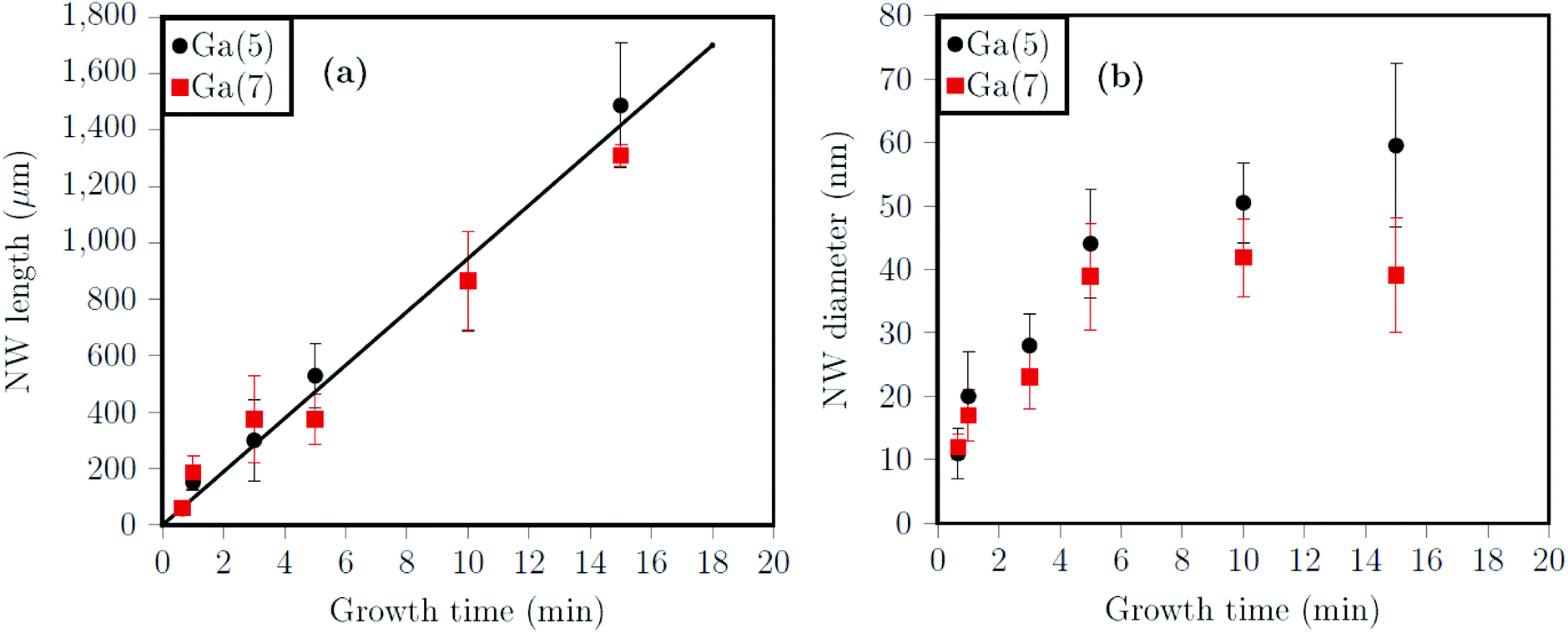 | ||
| Fig. 3 Graphics of (a) the NW length and (b) diameter as a function of the growth time including the data for short growths (20 s to 3 min). Black and red points correspond to Ga(5)As NWs and Ga(7)As NWs, respectively. The black line in (a) is a guide for the eyes for both black and red points. | ||
On the contrary, Fig. 3(b) shows that the trend for the evolution of the diameter is quite different. A rapid increase (≃5 nm min−1) of the diameter is observed for both Ga(5)As and Ga(7)As NWs for the shortest growth times (20 s to 5 min), whereas for the longest ones the Ga(5)As NWs show a linear radial growth rate (≃1 nm min−1), while their Ga(7)As counterparts present an almost constant one. For both cases, the NW diameter increase during the axial growth leads to NWs with an inverse tapered geometry. The different behaviors observed between short and long growth times are thus confirmed by the measurement of the tapering coefficient T% of the NWs, as defined by Colombo et al.,29 which results equal to 4–6% with shorter growth times and to 0.5–1% with longer ones, for both Ga(5)As and Ga(7)As NWs. This demonstrates that the radial growth compensating for the tapering effect is higher for the longer growth times (for which the diameter increase is low) than for the short ones (for which such an increase in diameter is higher). It should also be noticed that the NW diameter at the nucleation, occurring after about 12 s of growth, is ≃15 nm and corresponds to the average diameter of the Ga droplets as observed before the NW nucleation (cf. Fig. 4 in the ESI†).
3 Quantitative estimates
Due to the nature of the substrate surface (epi-ready SiO2 terminated Si substrate) and due to the low density of NWs in our experiments, in the following we shall (i) neglect the re-emission and shadowing effects for Ga atoms and (ii) consider that among the various sources of Ga and As atoms that supply the droplet we shall only take into account the simplest: direct impingement of both Ga and As atoms, and diffusion of Ga adatoms on the substrate and on the NW facets. As estimates based on experimental data show that the direct impingement of As atoms is not sufficient to support the growth process so that, following an assumption already proposed in ref. 35 we shall also include a fixed amount of re-emitted As atoms.While the microscopic features of the NW growth by the layer-by-layer mechanism depend strongly on the crystal structure of the materials involved, and are accompanied by oscillations in both the droplet concentrations and the truncated facet under the droplet,20 we shall adopt here an effective (macroscopic) point of view, limiting our study to the evolution of the NW length and diameter. Meanwhile, we still account for both wetting angle evolution and direct or inverse tapering but do not relate them to Wz and/or ZB formation. The proposed model can be further refined to a small-scale approach so as to include the layer-by-layer mechanism and crystallographic features but for simplicity we present a minimal version.
By extending previous semi-analytical models3,25,28,30 proposed for Au-catalyzed and self-assisted III–V NWs, we report a description of the NW growth kinetics using generic Ga and As sources located with respect to the substrate normal at angles αGa and αAs respectively. The main original feature of our model is to assume that, in agreement with stability requirements,36 the wetting angle β of the Ga droplet can take only values in an interval (βmin, βmax) = (55°, 140°), and to associate mechanisms with these limit values that allow the NW diameter below the droplet to increase (or to decrease), resulting in inverse (or direct) tapering.
In order to identify the model parameters we shall use only the experimental data obtained for the NWs grown by using the Ga(5) source. Then, using these parameters, we simulate the NW growth using the Ga(7) source so as to compare the predicted values for both the axial growth and the changes of the NW diameter (under the droplet) with the above reported experimental data.
3.1 The capture surfaces for the Ga atoms
Based on ref. 3, 25, 28 and 30 we shall assume three distinct ways for the Ga atoms to supply the droplet (Fig. 4): (a) diffusion on the SiO2-terminated Si substrate, (b) diffusion along the NW facets and (c) direct impingement across the droplet surface. These three contributions can be estimated as follows: | ||
| Fig. 4 Geometry of the NW and droplet, generic flux position at angle α with respect to the substrate normal and diffusion lengths. | ||
(a) The amount of Ga atoms, further denoted as qsubGa, able to reach the droplet by surface diffusion on the SiO2-terminated Si substrate (which must be followed by diffusion along the NW facets) exists only as long as the NW length, further denoted as L(t), is such that L(t) < λfacet, where λfacet corresponds to an average diffusion length on the NW facets. Per time unit we have
| qsubGa(t) = FGaSsub(t), | (1) |
(b) The amount of Ga atoms able to reach the droplet by diffusion along the NW facets can be written as
| qfacetGa(t) = FGatanαGaSfacet(t), | (2) |
tanαGa is the value of the flux on a vertical surface when the nominal flux (i.e. the flux on the plane normal to the direction of the source) is FGa/cosαGa. Finally, the min function accounts for the NW length L(t) only for NWs with length lower than λfacet.
(c) The amount of Ga atoms supplying the droplet by direct impingement is
 | (3) |
αGa accounts for the position of the source and the factor S(αGa, β(t), r(t)) is the exact value of the droplet area projected in the direction normal to the flux when the wetting angle of the droplet is β(t) and the droplet is located on top of a NW with radius r(t), as reported by Glas.37
3.2 The amount of As atoms supplying the droplet
By using the experimental data for the Ga(5)As NWs and a piecewise linear interpolation for the NW radius and length, we can estimate the amount of As atoms needed to grow the Ga(5)As NWs at t = 80 min aswhere aGaAs is the lattice parameter of ZB GaAs. We point out here that the values of the NW diameter reported in Fig. 1 do not include the vapor–solid NW radial growth contribution. Moreover, as the experimental results show that the Ga(5)As NW diameter is constantly increasing, we can deduce that, except at very early stages of the growth process, the droplet wetting angle value equals its maximum one βmax experimentally measured in the 138–142° range (see Fig. 2). With respect to previous models in ref. 3, 25, 28 and 30, the existence of a maximum (minimum) value for the droplet wetting angle is a feature of our model that allows including (as described below) a mechanism of increase (decrease) of the NW radius under the droplet.

If the incorporation of As atoms supplying the droplet is the result of only the direct impingement, then knowledge at time t of the NW radius r(t), the droplet wetting angle β(t), the As source incidence angle αAs and the nominal As4 flux FAs allows a straightforward computation that gives the amount of As atoms, NAs, supplying the droplet. In our case, an estimation by excess is

| qdropletAs(t) = (1 + ε)FAsS(αAs, β(t), r(t)), | (4) |
Obviously, the above description of Ga and As sources supplying the droplet holds in an isothermal process at a low density of NWs (in which case the shadowing effects can be neglected).
3.3 Growth mechanism description
We shall further assume that there is a critical concentration threshold,17 further denoted as c*, such that solidification occurs only if the droplet concentration c(t) ≥ c* (over-saturation). The growth process can be described as follows (see the ESI†):1. At fixed t let L(t), r(t), β(t) and c(t) be the NW length, NW radius, droplet wetting angle and As concentration in the droplet, respectively. The size and concentration of the droplet provide the amount of Ga and As atoms in the droplet, further denoted as QGa(t) and QAs(t). Then, during a small time-interval (t, t + Δt) we can update QGa(t) and QAs(t) so as to account for the amount of atoms supplying the droplet as described previously:
QGa(t) → ![[Q with combining circumflex]](https://www.rsc.org/images/entities/i_char_0051_0302.gif) Ga(t) = QGa(t) + (qsubGa(t) + qfacetGa(t) + qdropletGa(t))dt, Ga(t) = QGa(t) + (qsubGa(t) + qfacetGa(t) + qdropletGa(t))dt, | (5) |
| QAs(t) → As(t) = QAs(t) + qdropletAs(t)dt. | (6) |
2. The knowledge of Ga(t) and As(t) provides an estimate for the concentration as:
| ĉ(t) = As(t)/(Ga(t) + As(t)) |
2.1 The generic case occurs when the updated concentration is such that ĉ > c*. In this case there is a unique amount  of equal quantities of Ga and As atoms that can form a crystalline solid phase and such that for the remaining quantities QGa(t + Δt) = Ga(t) − Q(t) and QAs(t + Δt) = As(t) − Q(t) we obtain
| c(t + Δt) = QAs(t + Δt)/(QAs(t + Δt) + QGa(t + Δt)) = c*. | (7) |
Thus, both the NW length and diameter do increase with amounts that depend on both the solid material and the remaining liquid quantities: if QGa(t + Δt) and QAs(t + Δt) can form a droplet with β(t + Δt) < βmax, the NW grows only in the axial direction. If instead QGa(t + Δt) and QAs(t + Δt) cannot form a droplet with radius r(t) and wetting angle β(t + Δt) ≤ βmax, then both the increase of NW radius (under the droplet) and axial growth take place. In this case, the solid phase will modify both the NW radius and the NW length so as to fit the remaining liquid quantities QGa(t + Δt) and QAs(t + Δt) in a droplet with a wetting angle β(t + Δt) = βmax.
2.2 On the opposite, if ĉ ≤ c*, which may be the case if for instance qsubGa(t) + qNWGa(t) + qdropletGa(t) > qdropletAs(t), solidification will not occur but the droplet will change its volume. In this situation, the generic case occurs when the droplet increases its volume at a fixed NW radius. But it may happen that β(t) = βmax, so that the wetting angle cannot be increased further. In this case, a certain amount of Ga atoms cannot be incorporated into the droplet, because the pinning of the droplet on the NW top is unstable. The instability of the droplet pinned at the NW top can lead to various scenarios among which we cite: kinking induced by the wetting on the NW top and NW facets and/or droplet topology changes by separation. This situation is very similar to the one encountered when a droplet is supplied by Ga atoms only. In that case, since the wetting angle is bounded by βmax, incorporation of Ga atoms into the droplet stops at this value of the wetting angle. Decreasing the amount of Ga atoms that can be incorporated into the time-interval (t, t + Δt) increases the concentration ĉ(t). At the upper limit, when only As atoms supply the droplet, the droplet concentration ĉ(t) increases so that the NW length increases and the droplet decreases its volume. Similarly, at the lower limit, when due to solidification the liquid volume cannot fill a droplet with radius r(t) and wetting angle β(t + Δt) > βmin, the solid phase will decrease the NW radius so as to obtain the unique r(t + Δt) able to sustain the remaining volume at a wetting angle β(t + Δt) = βmin.
As proposed above, the model has 3 parameters: the two diffusion lengths λfacet and λSiO2 and the retro-diffusion factor ε. Previous models consider c* ≃ 0.01,17λfacet ≃ 1–5 μm (ref. 26 and 38) and λSiO2 ≃ 50−90 nm.18,39
We have implemented the above described model with initial conditions r(0) = 7.5 nm, c(0) = c* = 0.01 and β(0) = π/2, L(0) = 0 and compute the evolution of the NW length, the NW diameter, the droplet size and the wetting angle as well as the amount of Ga and As atoms incorporated into the droplet during the process for the Ga(5) source. The best results, presented in Fig. 5 (left), were obtained using the following parameters: λSiO2 ≃ 70 nm, λfacet ≃ 1.8 μm and ε = 0.13, in good agreement with previously cited references.18,26,38,39. Parameters obtained by the best fit using the Ga(5)As NWs experimental data were subsequently used to predict the length and diameter evolutions of the Ga(7)As NWs. The results are reported in Fig. 5 (right).
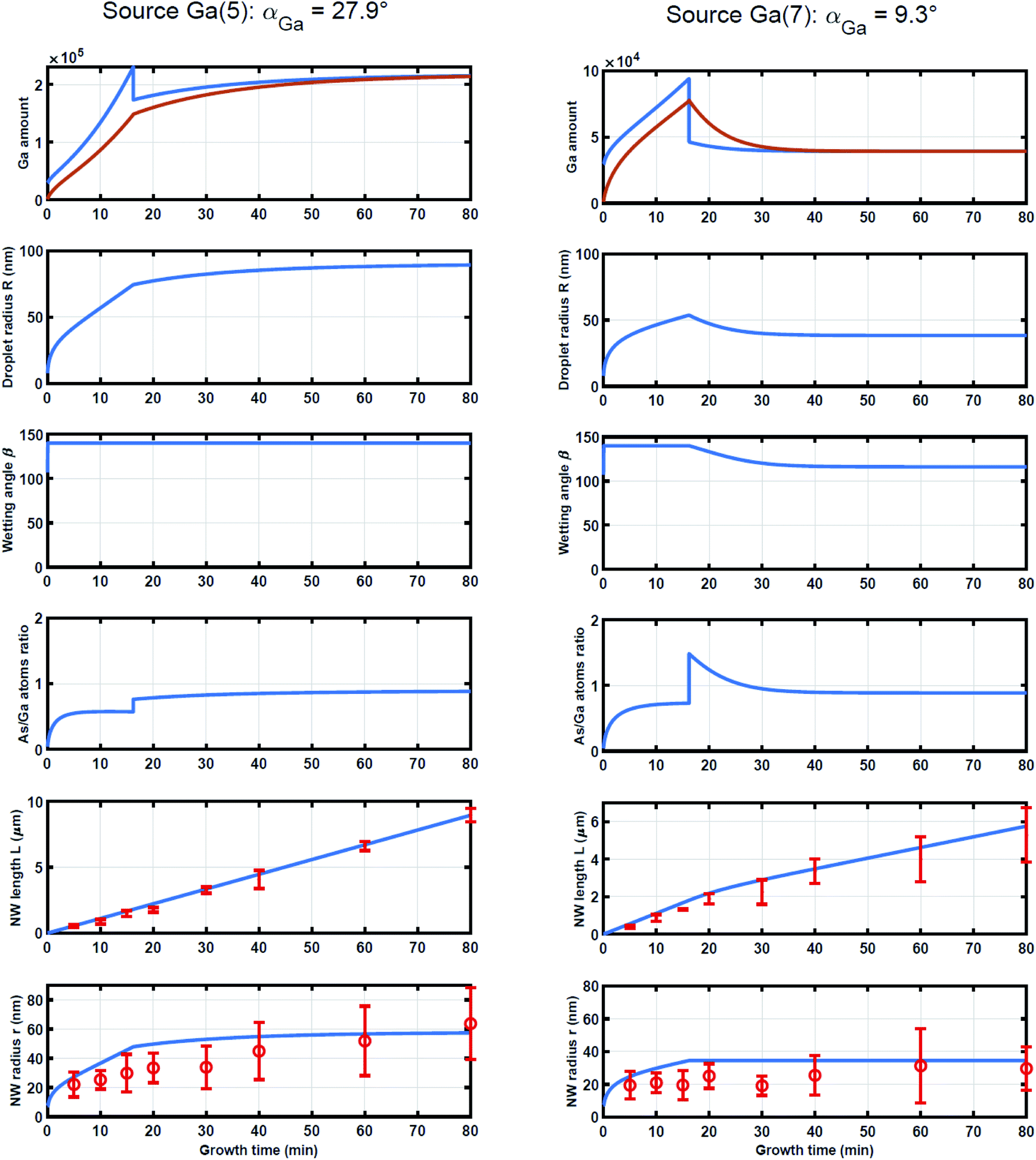 | ||
| Fig. 5 Numerical results (blues lines) obtained with the semi-empirical model for Ga(5) and Ga(7) sources. On the first line: the amount of Ga atoms supplying the droplet (in blue) and the amount of Ga atoms from the liquid droplet used for the NW growth (red) as a function of the growth time. On the next lines: the droplet radius, the wetting angle, the Ga/As ratio supplying the droplet, the NW length (computed – blue; experimental – red) and the NW radius (computed – blue and experimental – red). Numerical parameters are identified by fitting only the Ga(5) experimental data (left column). Using the same model parameters, but for the Ga(7) source, we have obtained the numerical results (blue lines) in the right column, plotted together with the experimental data (red points and error bars). | ||
We are now able to explain the main differences induced by the source position: at very short times (<1 min), starting with identical NW geometry and droplet size as well as identical Ga fluxes on planar surfaces, since the amount of As atoms captured by the droplet is very small, both Ga(5) and Ga(7) droplets increase their volumes. Meanwhile, even in this regime, the As amount is sufficient to supply the axial growth of the NW. But since the amount of Ga atoms exceeds the amount of As atoms, the critical wetting angle is rapidly attained (at ≃t ≃ 20 s as shown in Fig. 3 in the ESI†) for both sources as the droplet radius R(t) increases. As the NW length increases, the amount of Ga atoms supplying the droplet from diffusion over the NW facets from the Ga(5) source is about 3 times more important than that from the Ga(7) source. This quantity becomes dominant for the droplet supplied by the Ga(5) source while for that supplied by the Ga(7) source it has the same order of magnitude as the amount coming from diffusion on the substrate.
As shown in Fig. 5, due to the high FAs/FGa ratio, the amount of As atoms supplying the droplet has the same order of magnitude as the amount of Ga atoms for both sources all along the growth process. This means that all As atoms supplying the droplet are transferred to the solid phase at each time step. But the remaining liquid phase contains fewer Ga atoms with the Ga(7) source than those with the Ga(5) source so, as a consequence, the increase of the NW diameter (under the droplet) of the Ga(7)As NWs is slower than that of Ga(5)As NWs. In turn, this implies that gradually the size of the droplet for the Ga(5)As NWs increases faster than that of the Ga(7)As NWs. The higher the droplet radius, the higher the amount of As atoms supplying the droplet, and this explains the faster axial growth of the Ga(5)As NWs with respect to Ga(7)As NWs for t > 17 min.
At t ≃ 17 min, corresponding to L = 1.8 μm, when the length of the NWs overcomes the diffusion length on the NW facets, a large amount of Ga supplying the droplet is gradually lost, but since the Ga flux on the NW facets with the Ga(5) source is higher than the Ga atoms lost for the NW growth, this is not a significant event for Ga(5)As NWs. For the Ga(7)As NWs, the As/Ga ratio becomes suddenly greater than 1 and, as a consequence, additional Ga atoms from the droplet will be used for solidification at each time step. As shown in Fig. 5 (right), for Ga(7)As NWs the NW diameter stops to increase, the wetting angle decreases and the axial growth rate decreases accordingly.
The sudden loss of the Ga atoms supplying the droplet from substrate diffusion at t ≃ 17 min is actually a smoother transition between a regime dominated by the Ga atoms supplying the droplet from diffusion on the substrate and a regime dominated by the Ga atoms supplying the droplet from diffusion on the NW facets. Including this transition in the model will affect the local (in time) length and radius values but will have non-significant impact on the qualitative results.
These considerations highlight the importance of the Ga adatom diffusion on the substrate, without which a large part of the Ga collected by the droplet would be missing and the experimental data could not be explained. Such a result is consistent with models previously developed by others3,18,25,26,28,30 but it should be considered as specific for the diffusion of Ga adatoms on SiO2-terminated Si substrates, with a thin SiO2 surface layer 1–2 nm-thick, where the Ga adatom diffusion length is longer, whereas Ga adatoms can behave differently on thicker SiO2 masks (typically 10–20 nm-thick) used for substrate patterning,18 as shown elsewhere.23,34
It is interesting to notice that, in agreement with results in ref. 7 and 30, both classes of NWs evolve toward a stationary growth regime when the amounts of As and Ga atoms are identical and the growth mode is only axial. This asymptotic behavior is determined by two main factors: the fact that the V/III flux ratio is greater than 1 and the existence of a diffusion length for Ga adatoms along the NW facets. This is easily understood in a simplified framework when the NW radius is assumed constant but can be extended straightforwardly to variable NW radius growth models. Indeed, if the growth process is in a Ga-excess range, the droplet radius increases but since the V/III flux ratio is greater than 1, the system evolves toward a regime when the droplet is supplied with equal amounts of Ga and As atoms. On the opposite, in the As-excess range, the droplet decreases its volume and the direct flux amount on the droplet decreases for both species. However, since the droplet has an additional source of Ga atoms from NW facet diffusion, the system will evolve again toward a regime where the droplet is supplied with equal amounts of Ga and As atoms. These two arguments hold also when the NW radius evolves during the growth. The main reason for this is that the amount of atoms supplying the droplet from the direct flux scales (up to a bounded factor) like r2, while that of atoms attaining the droplet through the diffusion on the NW facets scales like r.
4 Conclusions
In conclusion, we experimentally demonstrated the influence of the incidence angle of the Ga flux on the growth kinetics of self-assisted GaAs NWs grown on SiO2-terminated Si substrates. The experimental results demonstrate that this growth parameter significantly affects the NW length and diameter evolution. Subsequently, we develop a model and performed numerical simulation so as to fully explain the experimental results.We developed a semi-empirical model and numerical simulations which highlight that the impact of the incidence angle of the Ga flux on the NW growth kinetics can be explained only by accounting for the contribution of Ga adatoms diffusing from the substrate surface to the Ga droplet. Such a result should be considered as specific for the diffusion of Ga adatoms on the epi-ready SiO2-terminated Si substrate, whereas Ga adatoms behave differently on patterned Si substrates with a thick SiO2 mask.
The second equally important factor is the diffusion length of the Ga adatoms on the NW facets. The role of such a contribution to supply the Ga droplet becomes important when the NW length overcomes such a value, so that the droplet cannot be supplied anymore by the adatoms diffusing from the substrate. It then becomes the main contribution to the droplet supply and, as expected, depends on the Ga flux incidence angle. As a consequence, the difference in length and diameter between GaAs NWs grown with different Ga flux incidence angles can be explained assuming that variations in Ga supply may cause a different response from the Ga droplet between the two cases once the NW length exceeds the diffusion length of Ga adatoms on the NW facets. This will modify the volume and shape of the Ga droplet, thus affecting the capture surface of As atoms and consequently, when the wetting angle of the Ga droplet becomes equal to a maximum value of typically 140°, it will modify both the NW axial growth rate and the NW diameter.
Ultimately, the results here reported show that the incidence angle of the Ga flux is an essential parameter to obtain good control over the self-assisted GaAs NWs grown by VLS-MBE. Such a result is quite significant, since it opens up to the possibility, having Ga cells with appropriately different incidence angles, of achieving fine control over the NW geometry and probably also over the NW crystal structure, by quickly modifying the amount of the incident Ga flux and therefore the amount of Ga supplying the droplet.
5 Experimental section
The samples subjected to this study were realized in a MBE reactor Riber 32 equipped with two Ga cells with different flux incidence angles respectively equal to 27.9° (denoted as the Ga(5) cell) and to 9.3° (denoted as the Ga(7) cell), and an As4 valved cracker cell with a flux incidence angle equal to 41°. All substrates employed for the growths consisted of 1 × 1 cm2 chips of boron-doped Si(111) (0.02–0.06 Ω cm) with an epi-ready surface oxide layer (≃1–2 nm-thick). The substrates were cleaned by sonication in acetone and ethanol for 10 min and degassed at 200 °C in ultra-high vacuum before introduction into the MBE reactor. In all cases 1 ML of Ga was pre-deposited at 520 °C always with the Ga(5) cell so as to form Ga droplets and, subsequently, pinned into the surface oxide layer when the substrate temperature was increased.40,41 The substrate temperature was subsequently increased up to 610 °C in 10 min and stabilized for 2 min. Then the substrate was exposed to Ga and As4 fluxes. As far as Ga is concerned, the flux in question originated either by the Ga(5) or the Ga(7) cell, but in any case the Ga flux adopted corresponded to a planar growth rate equal to 0.5 ML s−1, defined in terms of equivalent growth rate of a 2D GaAs layer grown on a GaAs substrate, as measured by reflection high energy electron diffraction (RHEED) oscillations. Similarly, the As4 flux was equal to an equivalent 2D GaAs layer growth rate5 of 1.15 ML s−1, thus providing an As/Ga flux ratio FAs/FGa = 2.3 for a GaAs growth on the substrate. The NW growths were finally stopped by closing the shutter of Ga and As4 cells simultaneously and rapidly decreasing the sample temperature, so as to preserve the Ga droplet on the NW top.Conflicts of interest
There are no conflicts to declare.Acknowledgements
The authors want to acknowledge the French Agence Nationale de la Recherche (ANR) for its funding to the HETONAN project (http://inl.cnrs.fr/projects/hetonan/). The authors thank G. Patriarche (C2N-CNRS, Palaiseau, France) for TEM images in Fig. 2 of the ESI,†J. B. Goure and C. Botella for technical assistance and the NanoLyon platform for access to the equipment.Notes and references
- F. Jabeen, V. Grillo, S. Rubini and F. Martelli, Nanotechnology, 2008, 19, 275711 CrossRef PubMed
.
- G. E. Cirlin, V. G. Dubrovskii, Y. B. Samsonenko, A. D. Bouravleuv, K. Durose, Y. Y. Proskuryakov, B. Mendes, L. Bowen, M. A. Kaliteevski, R. A. Abram and D. Zeze, Phys. Rev. B: Condens. Matter Mater. Phys., 2010, 82, 035302 CrossRef
- P. Krogstrup, R. Popovitz-Biro, E. Johnson, M. H. Madsen, J. Nygård and H. Shtrikman, Nano Lett., 2010, 10, 4475–4482 CrossRef CAS PubMed
- S. Plissard, G. Larrieu, X. Wallart and P. Caroff, Nanotechnology, 2011, 22, 275602 CrossRef CAS PubMed
- D. Rudolph, S. Hertenberger, S. Bolte, W. Paosangthong, D. Spirkoska, M. Döblinger, M. Bichler, J. J. Finley, G. Abstreiter and G. Koblmüller, Nano Lett., 2011, 11, 3848–3854 CrossRef CAS PubMed
- E. Russo-Averchi, J. Vukajlovic Plestina, G. Tütüncüoglu, F. Matteini, A. Dalmau-Mallorquí, M. de la Mata, D. Rüffer, H. A. Potts, J. Arbiol, S. Conesa-Boj and A. Fontcuberta i Morral, Nano Lett., 2015, 15, 2869–2874 CrossRef CAS PubMed
- V. Dubrovskii, T. Xu, A. D. Álvarez, S. Plissard, P. Caroff, F. Glas and B. Grandidier, Nano Lett., 2015, 15, 5580–5584 CrossRef CAS PubMed
- J. Vukajlovic-Plestina, W. Kim, L. Ghisalberti, G. Varnavides, G. Tütüncuoglu, H. Potts, M. Friedl, L. Güniat, W. Carter and V. Dubrovskii,
et al.
, Nat. Commun., 2019, 10, 869 CrossRef CAS PubMed
- D. Lang, H. Grimmeiss, E. Meijer and M. Jaros, Phys. Rev. B: Condens. Matter Mater. Phys., 1980, 22, 3917 CrossRef CAS
- M. Bar-Sadan, J. Barthel, H. Shtrikman and L. Houben, Nano Lett., 2012, 12, 2352–2356 CrossRef CAS PubMed
- M. J. Tambe, S. Ren and S. Gradecak, Nano Lett., 2010, 10, 4584–4589 CrossRef CAS PubMed
- S. Breuer, C. Pfüller, T. Flissikowski, O. Brandt, H. T. Grahn, L. Geelhaar and H. Riechert, Nano Lett., 2011, 11, 1276–1279 CrossRef CAS PubMed
- J. B. Jackson, D. Kapoor, S.-G. Jun and M. S. Miller, J. Appl. Phys., 2007, 102, 054310 CrossRef
- V. Schmidt, J. V. Wittemann, S. Senz and U. Gösele, Adv. Mater., 2009, 21, 2681–2702 CrossRef CAS
- V. G. Dubrovskii, G. Cirlin, N. Sibirev, F. Jabeen, J.-C. Harmand and P. Werner, Nano Lett., 2011, 11, 1247–1253 CrossRef CAS PubMed
- X. Yu, H. Wang, J. Lu, J. Zhao, J. Misuraca, P. Xiong and S. von Molnár, Nano Lett., 2012, 12, 5436–5442 CrossRef CAS PubMed
- F. Glas, M. R. Ramdani, G. Patriarche and J.-C. Harmand, Phys. Rev. B: Condens. Matter Mater. Phys., 2013, 88, 195304 CrossRef
- P. Krogstrup, H. I. Jørgensen, E. Johnson, M. H. Madsen, C. B. Sørensen, A. F. i Morral, M. Aagesen, J. Nygård and F. Glas, J. Phys. D: Appl. Phys., 2013, 46, 313001 CrossRef
- V. Dubrovskii, Appl. Phys. Lett., 2014, 104, 053110 CrossRef
- D. Jacobsson, F. Panciera, J. Tersoff, M. C. Reuter, S. Lehmann, S. Hofmann, K. A. Dick and F. M. Ross, Nature, 2016, 531, 317 CrossRef CAS PubMed
- E. S. Koivusalo, T. V. Hakkarainen, M. D. Guina and V. G. Dubrovskii, Nano Lett., 2017, 17, 5350–5355 CrossRef CAS PubMed
- W. Kim, V. G. Dubrovskii, J. Vukajlovic-Plestina, G. Tuĺtuĺncuĺoglu, L. Francaviglia, L. Guĺniat, H. Potts, M. Friedl, J.-B. Leran and A. Fontcuberta i Morral, Nano Lett., 2017, 18, 49–57 CrossRef PubMed
- F. Oehler, A. Cattoni, A. Scaccabarozzi, G. Patriarche, F. Glas and J.-C. Harmand, Nano Lett., 2018, 18, 701–708 CrossRef CAS PubMed
- J.-C. Harmand, G. Patriarche, F. Glas, F. Panciera, I. Florea, J.-L. Maurice, L. Travers and Y. Ollivier, Phys. Rev. Lett., 2018, 121, 166101 CrossRef CAS PubMed
- V. Dubrovskii, G. Cirlin, I. Soshnikov, A. Tonkikh, N. Sibirev, Y. B. Samsonenko and V. Ustinov, Phys. Rev. B: Condens. Matter Mater. Phys., 2005, 71, 205325 CrossRef
- V. Dubrovskii, N. Sibirev, R. Suris, G. Cirlin, V. Ustinov, M. Tchernysheva and J. Harmand, Semiconductors, 2006, 40, 1075–1082 CrossRef CAS
- F. Glas, J.-C. Harmand and G. Patriarche, Phys. Rev. Lett., 2007, 99, 146101 CrossRef PubMed
- M. Tchernycheva, L. Travers, G. Patriarche, F. Glas, J.-C. Harmand, G. E. Cirlin and V. G. Dubrovskii, J. Appl. Phys., 2007, 102, 094313 CrossRef
- C. Colombo, D. Spirkoska, M. Frimmer, G. Abstreiter and A. Fontcuberta i Morral, Phys. Rev. B: Condens. Matter Mater. Phys., 2008, 77, 155326 CrossRef
- V. Dubrovskii, N. Sibirev, J. Harmand and F. Glas, Phys. Rev. B: Condens. Matter Mater. Phys., 2008, 78, 235301 CrossRef
- P. Krogstrup, S. Curiotto, E. Johnson, M. Aagesen, J. Nygård and D. Chatain, Phys. Rev. Lett., 2011, 106, 125505 CrossRef PubMed
- E. Galopin, L. Largeau, G. Patriarche, L. Travers, F. Glas and J. Harmand, Nanotechnology, 2011, 22, 245606 CrossRef CAS PubMed
- K. Hestroffer and B. Daudin, J. Appl. Phys., 2013, 114, 244305 CrossRef
- M. Vettori, V. Piazza, A. Cattoni, A. Scaccabarozzi, G. Patriarche, P. Regreny, N. Chauvin, C. Botella, G. Grenet and J. Penuelas,
et al.
, Nanotechnology, 2018, 30, 084005 CrossRef PubMed
- M. R. Ramdani, J. C. Harmand, F. Glas, G. Patriarche and L. Travers, Cryst. Growth Des., 2012, 13, 91–96 CrossRef
-
J. W. Gibbs, The Collected Works of J. Willard Gibbs., Yale Univ. Press, technical report, 1948 Search PubMed
- F. Glas, Phys. Status Solidi B, 2010, 247, 254–258 CrossRef CAS
- P. Schroth, J. Jakob, L. Feigl, S. M. Mostafavi Kashani, J. Vogel, J. Strempfer, T. F. Keller, U. Pietsch and T. Baumbach, Nano Lett., 2017, 18, 101–108 CrossRef PubMed
- M. Shibata, S. S. Stoyanov and M. Ichikawa, Phys. Rev. B: Condens. Matter Mater. Phys., 1999, 59, 10289 CrossRef CAS
- M. H. Madsen, M. Aagesen, P. Krogstrup, C. Sørensen and J. Nygård, Nanoscale Res. Lett., 2011, 6, 516 CrossRef PubMed
- T. Tauchnitz, T. Nurmamytov, R. Huĺbner, M. Engler, S. Facsko, H. Schneider, M. Helm and E. Dimakis, Cryst. Growth Des., 2017, 17, 5276–5282 CrossRef CAS
Footnotes |
| † Electronic supplementary information (ESI) available. See DOI: 10.1039/c9na00443b |
| ‡ Current address: Physics Department, Lancaster University, Bailrigg, Lancashire LA1 4YW, UK. |
| § The 12.7% missing As atoms are computed with respect to the total amount of As needed; the retro-diffusion coefficient represents the % of the same quantity with respect to the total amount of As from direct impingement. |
| This journal is © The Royal Society of Chemistry 2019 |