
 Open Access Article
 This Open Access Article is licensed under a Creative Commons Attribution-Non Commercial 3.0 Unported Licence
All-dielectric concentration of electromagnetic fields at the nanoscale: the role of photonic nanojets
Jinlong
Zhu
 * and
Lynford L.
Goddard
* and
Lynford L.
Goddard
Photonic Systems Laboratory, Department of Electrical and Computer Engineering, University of Illinois at Urbana-Champaign, 208 N. Wright St., MNTL 2231, Urbana, IL 61801, USA. E-mail: zhuwdwz1@illinois.edu
First published on 11th November 2019
Abstract
The photonic nanojet (PNJ) is a narrow high-energy beam that was originally found on the back side of all-dielectric spherical structures. It is a unique type of energy concentration mode. The field of PNJs has experienced rapid growth in the past decade: nonspherical and even pixelized PNJ generators based on new physics and principles along with extended photonic applications from linear optics to nonlinear optics have driven the re-evaluation of the role of PNJs in optics and photonics. In this article, we give a comprehensive review for the emerging sub-topics in the past decade with a focus on two specific areas: (1) PNJ generators based on natural materials, artificial materials and nanostructures, and even programmable systems instead of conventional dielectric geometries such as microspheres, cubes, and trihedral prisms, and (2) the emerging novel applications in both linear and nonlinear optics that are built upon the specific features of PNJs. The extraordinary features of PNJs including subwavelength concentration of electromagnetic energy, high intensity focusing spot, and lower Joule heating as compared to plasmonic resonance systems, have made PNJs attractive to diverse fields spanning from optical imaging, nanofabrication, and integrated photonics to biosensing, optical tweezers, and disease diagnosis.
 Jinlong Zhu | Dr. Jinlong Zhu obtained his B.Sc. and PhD in Mechatronic Engineering from Huazhong University of Science and Technology, Wuhan, China. He is presently working at the Department of Electrical and Computer Engineering at the University of Illinois at Urbana-Champaign as a Post-Doctoral researcher. His research interests involve optical metrology, nanoscale sensing, semiconductor defect inspection, chiral photonics, integrated photonics, inverse problem, and topology optimization. He is co-author of over 50 publications and 10 patents. |
 Lynford L. Goddard | Lynford Goddard is a professor of Electrical and Computer Engineering at the University of Illinois. His group fabricates, tests, and models photonic sensors, circuits, and instrumentation, develops novel device processing techniques, and applies quantitative phase microscopy for nanoscale science and for semiconductor wafer metrology. He received the Presidential Early Career Award for Scientists and Engineers (PECASE) in 2010 and the AAAS Early Career Public Engagement Award in 2011. He is co-author of over 200 publications and 12 patents. |
1. Introduction
We start the review without a detailed discussion of well-known underlying theories for photonic nanojets (PNJs) such as Mie scattering and index limitation. Instead, we organize the article with a viewpoint on the generation and application of PNJs with the hope of stimulating new directions for future research.The nanoscale concentration of light in the visible and near-infrared (IR) spectral regions enables the re-examination of conventional rules for light–matter interactions and thus, lies at the heart of revolutionary photonic devices. The most well-known demand for nanoscale concentration of light undoubtedly comes from the semiconductor industry. Because of their wider bandwidth, photonic devices can replace electronic devices provided they can be densely integrated.1 However, delivering electromagnetic energy through conventional photonic devices (e.g., optical waveguides and photonic crystals) in a volume comparable to that of electronic devices manufactured at advanced technology nodes is non-trivial. Specifically, electromagnetic waves with the vacuum wavelength λ cannot last long in a dielectric cavity of characteristic size smaller than λ/2n, because the self-sustaining oscillations (i.e., the balance in the potential energy transfer) between the electric field energy and magnetic field energy of electromagnetic waves cannot be supported in the cavity.2 This phenomenon can be more briefly understood as the fundamental diffraction limit of light.
However, if we introduce free carriers in the cavity, the potential energy can also be stored in the form of kinetic energy of free carriers, making it possible to restore the balance of energy transfer. This is the physical fundament of why visible and IR light can be concentrated into regions with nanoscale characteristic sizes using metallic objects. Without any doubt, the research on plasmon-assisted concentration of light into nanoscale volumes will remain as one of the hot fields (along with metamaterials) because of its revolutionary potentials in many fields like microscopy,3 sensing,4,5 and integrated circuits.6 By propagating a mid-IR surface wave along a tapered two-wire transmission line, nanoscale IR spot with a diameter of 60 nm (λ/150) was observed using a nearfield microscope.7 Nanoscale focusing with a 2 × 5 nm2 footprint and an intensity enhancement of 3.0 × 10⁴ was achieved in an Au–SiO2–Au gap plasmon waveguide using a carefully engineered three-dimensional taper.8 Im et al. described a high-throughput, label-free plasmonic exosome assay for quantitative analysis of exosomes.9 Liu et al. introduced a far-field optical superlens capable of imaging beyond the diffraction limit via converting the evanescent waves into propagating waves, which can be measured in the far field.10 However, although surface plasmon polaritons of metallic structures (especially Au and Ag, whose scattering rate are 12.32 × 10¹³ s−1 and 3.6 × 10¹³ s−1, respectively) have been conceptually applied to create many novel devices or to boost the performance of existing mechanisms, the extremely high-loss in metallic materials typically makes high-efficiency plasmonic-based photonic devices impractical. The few exceptions have been in imaging and sensing, where sensitivity is more critical than efficiency. A highly doped semiconductor is a promising alternative to metals, but ωp for a semiconductor is an order of magnitude lower, thereby limiting them to the mid-IR and longer wavelengths.2,11 Gain materials to compensate metal loss have been researched, but theoretical computations show that extremely high power is required. For those reasons, in recent years, interest has grown in using non-metallic, all-dielectric materials to pull off some of the same light-localization tricks enabled by plasmonics while avoiding the tendency of plasmonic systems to dissipate optical energy as heat.12
The trick in all-dielectric light concentration at the nanoscale is that although light cannot be squeezed in a sub-wavelength cavity, it can be tailored in all three dimensions outside of dielectric structures via the contribution from evanescent waves or via purely the interference of propagating waves.13 More importantly, nanostructured dielectric materials with a high value of the refractive index offer a novel way to directly engineer a magnetic field response at optical frequencies in addition to the electric field response in plasmonic structures. These features of dielectric nanostructures have recently risen to prominence in the nanophotonics toolkit for diverse fields by creating electric or magnetic hot spots. Albella et al. investigated the possibility of utilizing the field-enhancement in the nanogap of silicon dimers for the fluorescence of either electric or magnetic emitters.14 Shcherbakov et al. demonstrated ultrafast all-optical switching in subwavelength nonlinear dielectric nanostructures exhibiting localized magnetic Mie resonances.15 Regmi et al. demonstrated the effectiveness of an approach using the field hot spots created by silicon dimers to enhance the fluorescence detection of single molecules.16 The creation of nanoscale hot spots through the engineering of dielectric nanostructures in the near-field region arises from the interference and diffraction nature of various components of light (especially the evanescent ones); thus, an interesting way to create deep subwavelength hot spots in the far-field via the propagating components only, is based on superoscillation theory,17–19 which has been successfully applied into the area of super-resolution imaging. Although the aforementioned metasurfaces are capable of tailoring the light field for nanoscale localization or focusing either in the near-field or far-field, the complicated processes required in the fabrication of metasurfaces hinder the generalization and industrialization for diverse applications. One may ask, are there any nanostructures that behave similar to metasurfaces in terms of squeezing the light but have much simpler geometrical profiles? Actually, we do have, and the answer is quite straightforward, i.e. the slot waveguides.20 A slot waveguide can guide strongly confined light in the nanoscale low refractive index gap by total internal reflection. The underlying physics, i.e., the discontinuity of the electric field (E-field) at high-refractive-index-contrast interfaces,21 can be somehow related to the physical fundaments of the hot spots created in the nanoscale dimers.15 However, the realization of nanometer scale localization of electromagnetic fields pays the price of rigid excitation conditions (i.e., fiber-coupled laser coupling or grating-based coupling) and long transverse length. For all those reasons, we do need a type of simple, non-metallic, massively manufacturable, and small-in-dimension structures that concentrates light to nanoscale volumes for various types of excitation mechanisms including free-space beams and fiber or waveguide-coupled modes.
Surprisingly, the natural world has provided us the answer: spheres, which are the most universal and simple geometries in nature and can be found from celestial bodies to atoms, can meet all the rigid conditions as mentioned earlier when they interact with light: microscale or even nanoscale dielectric spheres with the refractive index smaller than two, can concentrate free-space beams or waveguide modes impinging from any spatial direction to deep subwavelength volumes. Actually, it's been known since ancient times that a garden should not be watered in the afternoon, as the small droplets of water deposited on the leaves could cause sunburns.22 Yet, the thorough investigation of the narrow, non-resonant, and highly spatially confined optical field emerging on the shadow side surface of microspheres with diameters comparable to or somewhat larger than the wavelength of the incident optical radiation, was not implemented until 2004, when Chen et al. coined the terminology “photonic nanojet” for the concentrated field. Although microspheres do have similar geometrical features with those of a macroscopic lens or a conventional micro-lens, the rigorous analysis through Mie theory combined with Debye series have demonstrated that the behavior of the microsphere is significantly different from that of the conventional solid immersion lens in terms of the beam width, concentrated energy, and reaction to nanoscale perturbations.23,24 Such a difference can be somehow attributed to the size effect: microspheres that could generate PNJs, typically have the size in between Rayleigh particles and micro-lens; thus, one can use neither electrostatic approximation nor geometrical optics, but only the Mie scattering theory, to analytically disclose the underlying physics, in which, the unusual entanglement of propagating and evanescent components may be responsible for the uniqueness of PNJ properties.25 Here, we use the term “may be” because the underlying physics of some PNJ-based applications is still under debate, e.g., the PNJ-assisted super-resolution imaging,26 though there are already considerably numerical and experimental investigations.27–31 However, the mystery in the physics did not hinder the formation of a huge family of applications based on PNJs—we can now find the footprints of the PNJ in nearly all the major subjects related to nanophotonics, e.g., nanolithography, nanoscopy, fluorescence enhancement, sensing, photodetection, resonators, Raman and Stokes microscopy, optical data storage, transmission enhancement, waveguides, and all-dielectric switching. Although the term “PNJ” was originally coined for the concentrated beam regarding microspheres, it has been generalized immensely to also represent the squeezed field on the shadow surface of non-spherical objects, such as cuboids, triangles, gratings, and nanofiber assemblies.32–35 Such a generalization facilitates the explanation and description of the light–matter interaction for non-spherical objects in the PNJ language. The emergence of novel light sources including frequency combs,36 ultra-fast lasers,37 super-continuum sources,38 and quantum atom-fiber photonics,39 provide a brand-new dimension for the PNJ generators (microsphere and its derivatives) to manipulate light–matter interaction in extreme environments. For all these reasons, we do believe that the PNJ, which is promising in many fields in terms of efficiency, simplicity, manipulability, and manufacturability, will remain as an interesting and hot research topic. Hence, we do feel, a thorough review for disclosing new perspectives, unusual physics, and exciting trends, is of great importance to both new entrants in the field and people who are seeking to use it in interdisciplinary work. We should mention that different from previous review articles by Wang and Heifetz that primarily discuss PNJs formed by dielectric particles such as microspheres, microcylinders, and prisms,21,23 this article is more focused on disclosing the diversity in PNJ generators for both nature-inspired and metamaterials-based ones, as well as on the emerging novel applications of PNJs in both linear and nonlinear regimes in the past decade. The techniques (including index engineering, geometry engineering, and topology optimization) disclosed in Sec. 2 enables the customization of PNJ properties including FWHM, energy concentration, gradient field, and microlensing effects. The capability of customizing these properties of PNJ is critical to diverse applications of PNJs because each application requires one or several specific properties of PNJs.
2. Diversity in PNJ generators
2.1 Origin and theory of PNJs
The initial identification of the PNJ for a dielectric cylinder and a dielectric sphere was reported by Chen and Li, respectively.40,41 Applying a high-resolution finite-difference time-domain (FDTD) computational solution of Maxwell's equations or an exact eigenfunction series solution of Maxwell's equations in spherical coordinates (i.e., Mie theory), evidence was provided that both dielectric cylinders and spheres with microscale dimensions illuminated by a plane wave, can generate a narrow, high-intensity, sub-diffraction-waist beam (i.e., the PNJ) that propagates into the background medium from the shadow-side surface. By analogy with macroscopic components like cylindrical lenses and spherical lenses that are characterized by the geometrical optics, microscale cylinders and spheres theoretically concentrate plane waves with specific polarization states into a line and a point, respectively. Consider now such a cylindrical or spherical lens having a small but fixed f-number and shrinking down its dimensions to the microscale such that its focal length f becomes smaller than a fraction, a, of the wavelength λ, i.e.,| f < aλ. | (1) |
See the schematics in Fig. 1. When eqn (1) applies, the evanescent components of the scattering field cannot be neglected as can be done with macroscopic optics components. At a distance of λ/e, from the microlens, the power of the evanescent waves attenuates to 36.8% of its peak value. Moreover, for the scattering of visible and near-IR light via microscale objects, eqn (1) is usually much tighter than the inequality that relates to the Fraunhofer distance
| f < 2D2/λ, | (2) |
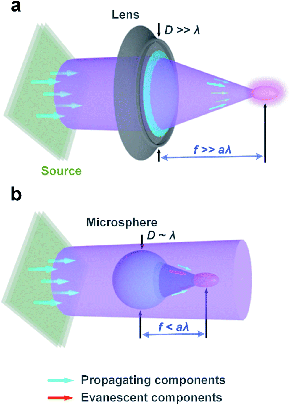 | ||
| Fig. 1 Schematics of the concentration for the plane-wave excitation based on (a) macroscale and (b) microscale objects. The ideal focal lengths shown in (a) and (b) are far larger and smaller than the wavelength, respectively. | ||
2.2 PNJ generators in the nature
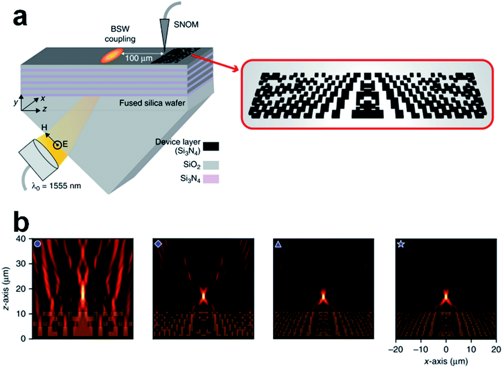
Theoretically, any spherical or cylindrical micro-object with the refractive index smaller than two can be a PNJ generator.21 Many building blocks of living organisms such as proteins, water, and carbohydrates have indices less than two in the visible regime (this is also the reason why the Born or Rytov approximation can be introduced to enable optical phase imaging for living cells without suffering from significant multiple scattering).46 This makes it possible to utilize natural materials to generate PNJs.47 It has been demonstrated that spider silk with a spherical cross-section can behave as a superlens for super-resolution imaging in contact mode at λ/6 scale, which is well beyond the classical limit [see Fig. 2(a)].48 It has been suggested that the phototaxis of Synechocystis cells may arise from the spherical microlens effect of the cells.49 In a macroscale imaging system, a high-NA objective lens enables optical trapping and sensing of nanoscale objects.50,51 Analogously, the microlens effect of cells make it possible to use a single cell to trap, image, and sense nanoparticles as was successfully demonstrated very recently.52 A significant difference to conventional optical imaging is that the single cell can be operated in contact mode such that the possible evanescence–propagation coupling can facilitate super-resolution imaging. See Fig. 2(b) showing the focusing effect of a single cell for red, green, blue (RGB) lasers and nanopattern imaging in scanning mode. In the field of optical tweezers, self-bonding is a phenomenon in which a cascade of objects forms as the result of the generation of a trapping potential through the trapped objects. A cell trapped at the tip of fiber concentrates the electromagnetic energy and forms a trapping potential to capture a second cell. “Chain reaction” form such that more and more cells become trapped until the trapping potential can no longer overcome the background perturbation. Such a phenomenon has been reported in several studies such as biophotonic waveguides, enhanced upconversion fluorescence, and near-field optical probing.46,53–55 See a bio-microlens trapped at the tip of a fiber that behaves as a PNJ generator to form a E. coli chain in Fig. 2(c). An interesting topic is how to achieve a tunable “biolens” such that its optical features match diverse applications. It has been shown that the red-blood-cell-based microlens can stretch the cell membrane with an enhancement factor of 1.5 in a noncontact and noninvasive manner.56 This enlightens the possibility of using a second PNJ to tune the geometric shape of a cell in order to achieve an adjustable biolens. A more straightforward method is to control the liquid buffer's chemistry such that the red blood cell can swell up from a disk shape to a sphere, leading to a varying focal length.57 As cells are typically operated in liquids, the aforementioned tunable techniques are limited to immersion environments.58 Moreover, the precise control over a biolens is challenging because a living microlens has diverse fundamental elements and thus its accurate optical response to external excitation is nonlinear and unknown.59 For these reasons, we will focus on the artificial-materials-based PNJ generators thereinafter. However, we should mention that the biolens will still find its unique value in many applications where man-made materials can hardly be applied, such as intravital trapping and sensing.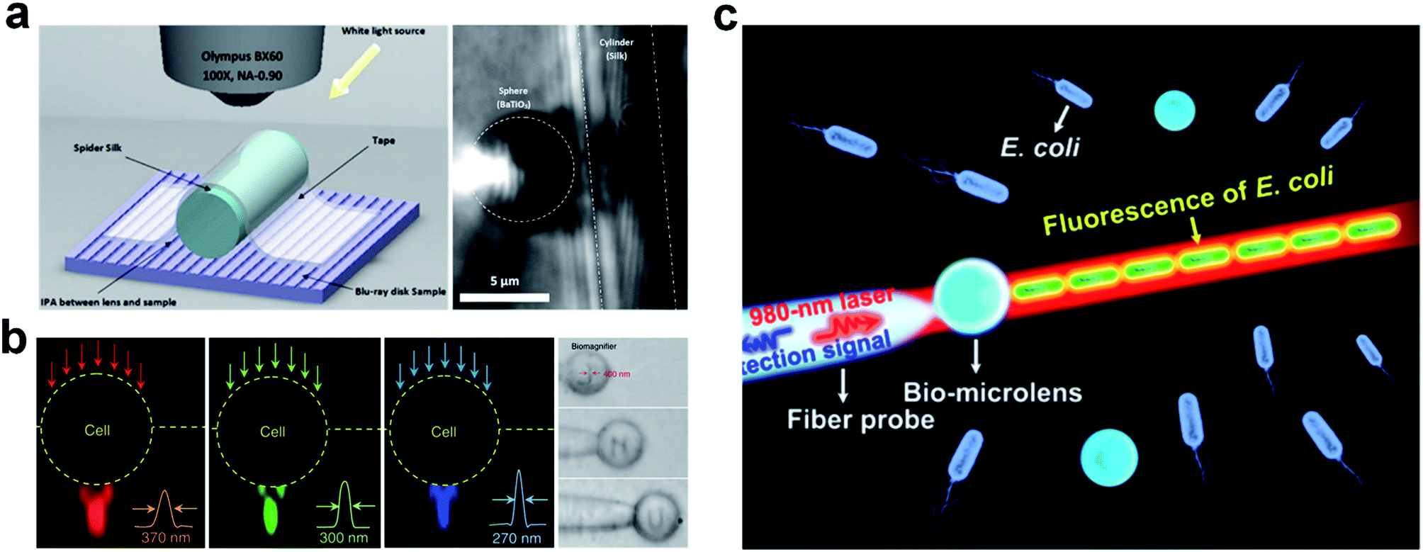 | ||
| Fig. 2 (a) Schematic diagram of silk biosuperlens imaging and super-resolution images of a Blu-ray disk in reflection mode. Reproduced with permission from ref. 48. Copyright 2016, American Chemical Society. (b) Darkfield images showing the focusing effect of a single cell for RGB lasers. Reproduced with permission from ref. 52. Copyright 2019, Nature Publishing Group. (c) Schematic showing the fluorescence enhancement of an E. coli chain originating from a bio-microlens. Reproduced with permission from ref. 53. Copyright 2017, American Chemical Society. | ||
2.3 Index engineering for PNJs
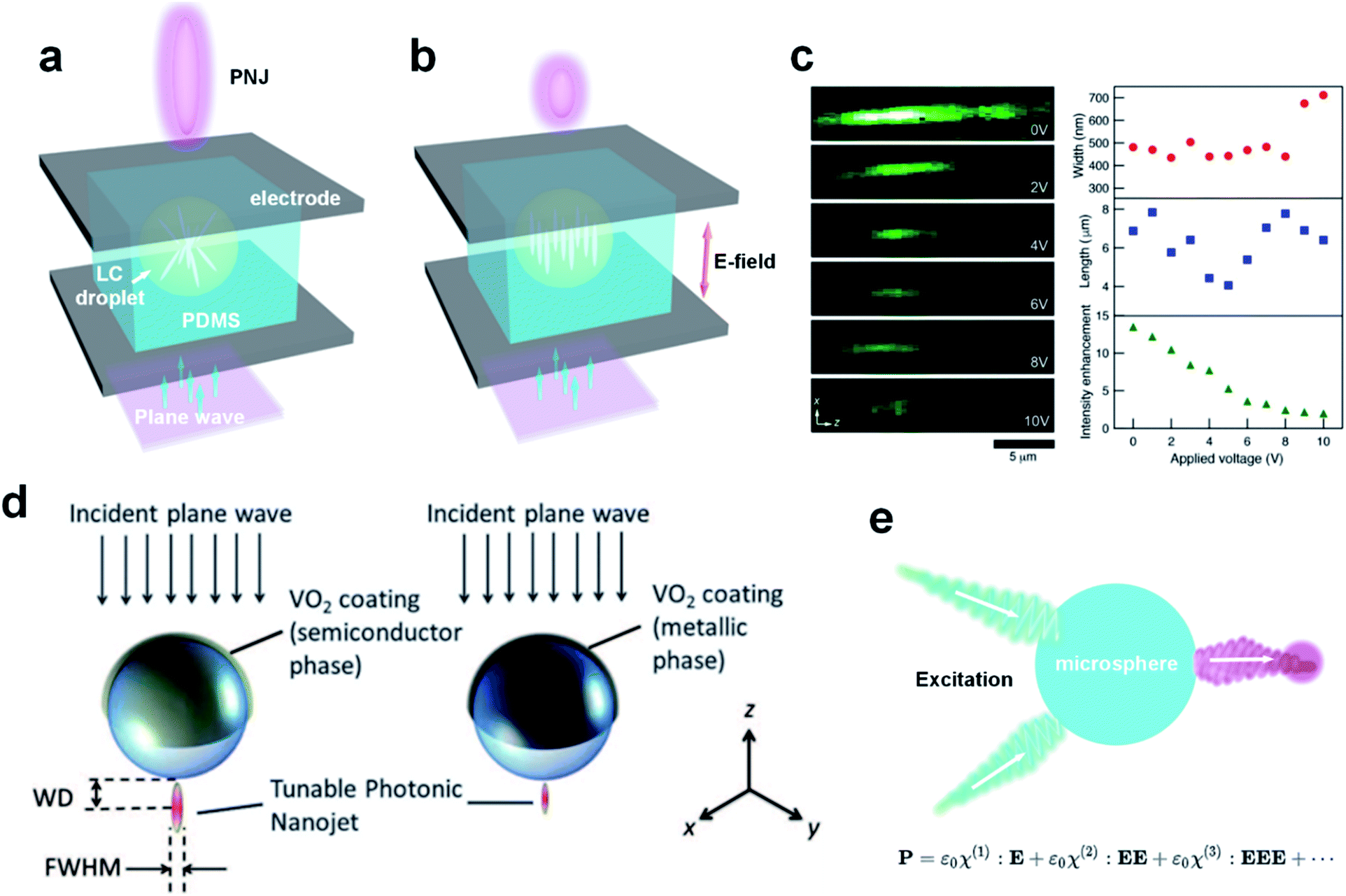
The refractive index determines the angle of refraction on an interface via the generalized Snell's law;60,61 thus, the most direct way to tune PNJs is via controlling the index of the PNJ generators. It has been shown numerically, as early as the year 2009, that a radially index-graded microsphere can increase the useful length of a PNJ by an order-of-magnitude to approximately 20 wavelengths, which is effectively a quasi-one-dimensional light beam. This may be useful for optical detection of naturally or artificially introduced nanostructures deeply embedded within biological cells.62 Actually, by analogy with macroscopic spherical lenses, one can anticipate, qualitatively, that reducing the index contrast between the microsphere and its surrounding ambient could longitudinally elongate the hot spot; however, rigorous numerical modelling is required to quantitatively validate the prediction because of the evanescent contribution and effects of diffraction.63 Two-dimensional and three-dimensional spherical microstructures are the most widely investigated objects for index engineering. Geints et al. considered dielectric spherical composite particles consisting of a core and several concentric shells having different refractive indices. The dependence of the longitudinal and latitudinal sizes of a PNJ and the PNJ's peak intensity on the optical contrast variation of the shells was numerically investigated. They showed that by properly changing the refractive indices of neighboring shells, it is possible to manipulate the PNJ shape and, particularly extend its longitudinal size or increase its peak intensity.64 Shen et al. showed that ultralong nanojets can be generated using a simple two-layer microsphere structure. In particular, they showed that for a glass-based two-layer microsphere, the PNJ has an extension of 22 wavelengths.65 A similar investigation of a liquid-filled hollow microcylinder under a liquid immersion condition was numerically investigated by Gu et al., in which they demonstrated super-long PNJs with decay lengths more than 100 times the illumination wavelengths in the outer near-field region of the microcylinder.66 Zhen et al. reported the realization of an ultranarrow PNJ, which is formed by a two-layer microcylinder of high refractive-index materials. They numerically showed that under 632.8 nm illumination, the full width at half maximum (FWHM) of the beam waist can reach 87 nm (∼λ/7.3), which appears to be the narrowest PNJ ever reported.67In fact, tuning the scattering by varying index contrast has a long history (for instance, the Luneburg lens,68 which is widely employed at microwave frequencies). But, what really makes the community excited is the capability of dynamically varying the index contrast for tuning the properties of PNJs, so that a single device can satisfy the needs of diverse applications. Possibly, the easiest and also the most direct way to tune is through liquid crystals (LCs). LCs have been extensively utilized in many fields including organic electronics and energy conversion, the creation of nanostructured materials or ordering nano- and microparticles, actuators, polymer-dispersed LCs, and spatial light modulators.69–73 Liu et al.,74 Matsui et al.,75 Eti et al.,76 and Du et al.,77 have investigated the properties of PNJs as functions of the phase transitions of LCs, but the first experimental imaging of tunable PNJs using LC control appears to have been achieved by Matsui and Tsukuda.78 In their experiments, a LC microdroplet formed in a polydimethylsiloxane (PDMS) matrix is sandwiched between indium-tin-oxide (ITO) electrodes. Applying external voltage to the device alters the alignment of the LC molecules [a nematic LC (E7, LCC)] in the droplet, which changes the effective refractive index, and thus the electro-tuning of the PNJ can be realized. See the schematic of the PNJ generator device in Fig. 3(a) and (b), and the reconstructed PNJ generated by a LC microdroplet under applied voltage viewed along the optical z axis, as measured by a confocal microscope. The three plots from top to bottom on the right-hand side of Fig. 3(c) represent the beam width, beam length, and intensity enhancement of the PNJ as a function of applied voltage, respectively.
 | ||
| Fig. 3 Schematic of tunable PNJ generator device with (a) off and (b) on states based on a LC microdroplet and (c) measured PNJ under different voltages viewed along the z axis. Reproduced with permission from ref. 78. Copyright 2017, Optical Society of America. (d) Schematic diagram showing the VO2-coated microsphere for 800 nm illumination. Reproduced with permission from ref. 84. Copyright 2016, Optical Society of America. (e) Our proposal for generating a tunable PNJ using nonlinear effects in a dielectric microsphere. | ||
The phase transition of LCs is not the only way to tune the properties of PNJs, but any other methods that modify the index distribution would work as well. For instance, phase change materials79–83 switch from their amorphous state to their crystalline state and vice versa. This provides a binary tuning of the index contrast. Soh et al. implemented a numerical investigation of how temperature can tune the FWHM and working distance (WD) of a PNJ generated by a glass microsphere whose top half-surface is coated with vanadium oxide (VO2), a phase change material.84 See the schematic in Fig. 3(d). As VO2 changes from semiconducting to metallic phase, the refractive index of the VO2 layer changes at its transition temperature of 68 °C. They found that a coating of 75 nm on a 5.0 μm diameter microsphere with a refractive index of 1.50 is optimal, as it tunes the FWHM the greatest while remaining thin enough to have a high transmission. When the temperature is raised from 20 °C to 90 °C, the FWHM varies from 0.43 μm to 0.37 μm, corresponding to a 14.0% change. The WD varies from 0.29 μm to 0.20 μm, corresponding to a 31.0% change. To enable the dynamic tuning of PNJs, one needs a reversible mechanism that facilitates the variation of indices in a continuous space. It has been demonstrated that the refractive index and optical band gap of CR-39 polymers in UV-visible range reduce as the annealing temperature increases,85 making it possible to use CR-39 polymer as the scaffold to design PNJ generators with tunable features via heating. Different to heat tuning, Yu et al. reported that the refractive index of transition metal dichacolgenide monolayers, such as MoS2, WS2, and WSe2, can be substantially tuned (by >60% in the imaginary part and >20% in the real part) around exciton resonances using complementary metal–oxide–semiconductor (CMOS) compatible electrical gating.86 However, the aforementioned mechanisms only work for specific materials and cannot be generalized to arbitrary ones because of different electro-optic and thermal-optic coefficients. The nonlinear optical effect is an inherent attribute of materials. Laser light with sufficiently strong power can result in a nonlinear response of a material system, i.e.,
| P(t) = ε0χ(1)E(t) + ε0χ(2)E2(t) + ε0χ(3)E3(t) + …, | (3) |
2.4 Geometry engineering for PNJs
Compared to index engineering, the customization of shapes for diverse PNJ applications is much easier to implement, owing to, at least partially, the advances in nanoscale fabrication.87–91 One typical advantage of geometry engineering is that the limitation of low-index materials (refractive index less than two) as required in conventional dielectric microspheres, can be conquered;92 however, the majority of PNJ generators use aspherically-shaped low-index materials (possibly, due to convention). The second reason for the bloom of geometry engineering is related to circumventing the drawbacks of PNJs generated by microspheres and microcylinders for specific applications.93 For example, to detect intrinsic nanostructures and artificially introduced nanoparticles that are deeply embedded within biological cells researchers requires a long PNJ length, whereas a rapidly convergent PNJ generated by the microsphere or microcylinder is followed by a fast divergence.77 We give, herein, a review on the major published results of the past decade on the geometry engineering for PNJs, to remind our readers of the diversity in PNJ customization.Geints et al. investigated the longitudinal and transverse dimensions of the PNJ as well as the dependence of its peak intensity on the optical contrast of micrometer-sized composite particles consisting of a nucleus and several shells with different refractive indices. It was shown that, the length and peak intensity of PNJs can be manipulated via varying the index contrast.94 Grojo et al. showed both numerically and experimentally that Bessel-like PNJs can be obtained with properly engineered sub-wavelength core–shell colloids.95 This form of geometry engineering is strongly inspired by a far-field approach for the generation of Bessel beams. Pacheco-Peña et al. demonstrated the ability of high-index dielectric hemispherical particles immersed in air to generate PNJs with extreme resolution (∼0.06λ).96 Huang et al. employed a genetic algorithm coupled with Mie theory to optimize the magnetic field intensity distribution of PNJs generated by multilayer microcylinders at visible wavelengths in free space.97 Zhou showed that a micro-gold tube illuminated by a TM-polarized plane wave could generate a stronger PNJ than that generated by dielectric cylinders with the same dimension.98 Hengyu et al. reported that a PNJ with a small FWHM of 0.398λ (λ = 0.4 μm) can be achieved by illuminating the curved side of a hemispheric shell possessing a high refractive index and properly chosen diameters and thickness.99 McCloskey et al. experimentally demonstrated that high intensity PNJs with nanoscale footprint and low divergence can be generated in a system of Si3N4 microdisks illuminated from the side with purple, green, and red laser light.100 Wu et al. reported that the features of a PNJ can be changed by decorating the dielectric microsphere surface with concentric rings.101 See the schematics of the decorated microspheres, the brightfield microscope, and fabricated samples shown in Fig. 4(a–c). They demonstrated that a FWHM waist of 0.485λ (λ = 0.4 μm) is achievable by engineering the microsphere with four rings etched to a depth of 1.2 μm and a width of 0.25 μm. Wu et al. further generalized the idea of decoration for microsphere surface by covering the center of a microsphere with a flat mask, to engineer PNJs.102 These works have demonstrated that both global and local modification for microspheres or microcylinders can significantly affect the properties of the generated PNJs.
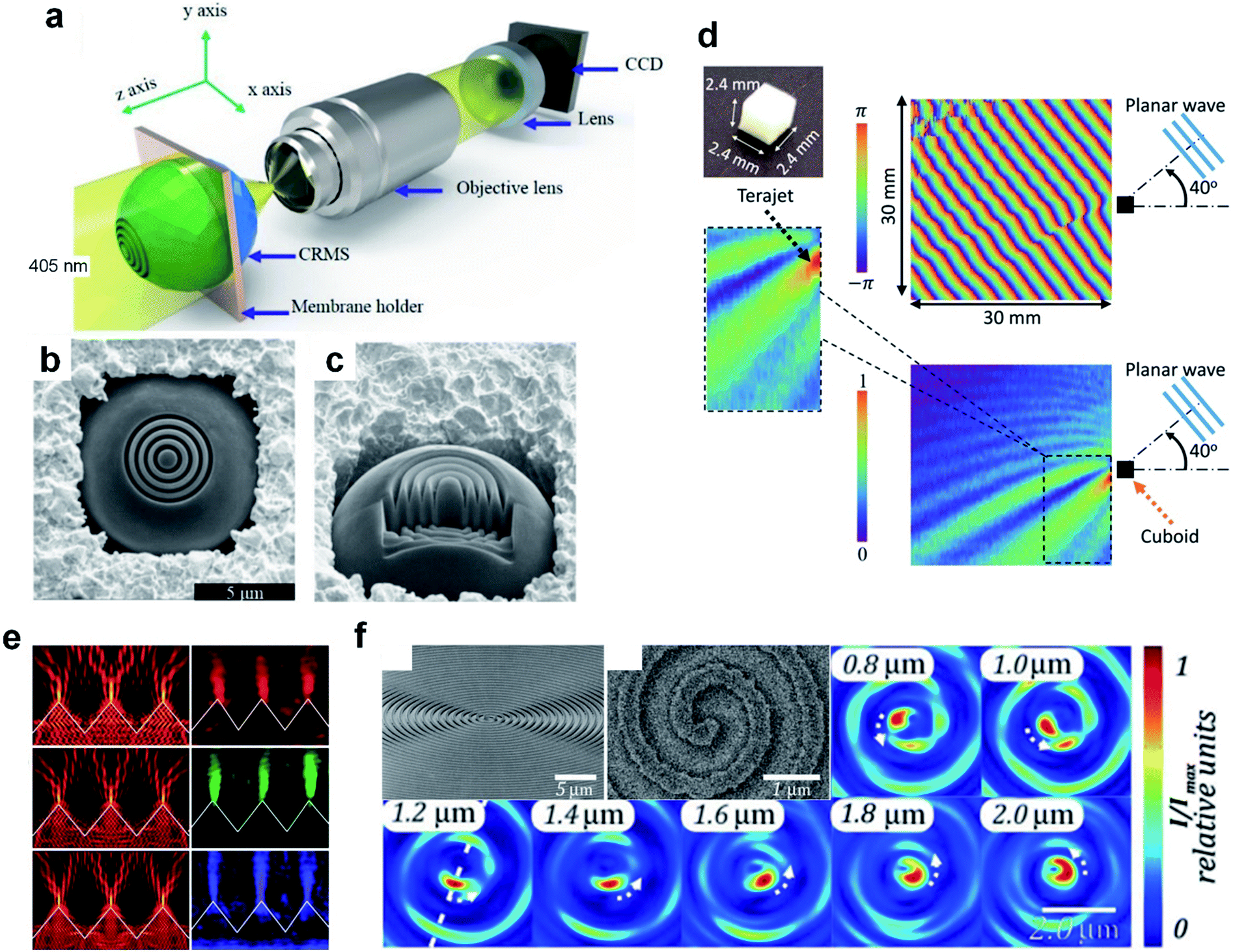 | ||
| Fig. 4 (a) Schematic of measuring a PNJ by a conventional optical microscope. The lens located between the objective lens and the CCD is the focusing lens. (b) Top and (c) side views of a microsphere decorated with 4 rings. Reproduced with permission from ref. 101. Copyright 2015, Optical Society of America. (d) A fabricated polytetrafluoroethylene cube and the experimental visualization of the phase and amplitude profiles of the PNJ. Reproduced with permission from ref. 109. Copyright 2017, American Institute of Physics. (e) Experimental images (right) and FDTD simulation (left) of power flow distributions for the diffraction gratings at incident wavelengths of 671 nm, 532 nm, and 405 nm. Reproduced with permission from ref. 113. Copyright 2018, Institute of Physics. (f) Side view and top view SEM images of the central part of the manufactured spiral axicon, and intensity distribution in the cross-sections at different distances from the axicon surface. Reproduced with permission from ref. 114. Copyright 2016, Optical Society of America. | ||
In fact, PNJs are not an exclusive feature of spherical objects, but many structures with aspherical edges have now been involved because of their capability in generating PNJs with distinct features. It has been shown experimentally that square-profile microsteps on a silica substrate, can produce sub-diffraction-limit PNJs with enhanced intensity near the surface via the illumination by a linearly polarized laser beam of wavelength λ = 633 nm.103 This device is similar to the dielectric cuboids being tested in various illumination modes.104–108 The dielectric cube can produce an asymmetric phase anomaly and Gouy phase shift at the terahertz frequency, which cannot be explained simply as an analogy to a lens focusing a Gaussian beam.109 See the cube and experimental results in Fig. 4(d). Zhang et al. proposed a microtoroid structure with high index (n = 3.5) to generate an ultralong PNJ.110 Geints et al. reported on the calculations of optical radiation scattering at micrometer-sized axicon particles and showed that PNJs with up to ∼25λ length are achievable without sacrificing high peak intensity and subwavelength transverse width.111 We can, undoubtedly, assemble the aforementioned individual PNJ generators as a periodic grating [see one of the representative images shown in Fig. 4(e)], so that massive arrays of PNJs can be generated simultaneously for diverse applications like sub-diffraction imaging, interferometry, and surface fabrication.34,112,113 Degtyarev et al. proposed an interesting extension for PNJs (i.e., the generation of a PNJ with a helix shape), which is called photonic nanohelix.114 See the image of the central part of the manufactured spiral axicon obtained with a scanning electron microscope (SEM) in Fig. 4(f). This potentially adds a new dimension to the optical manipulation of nanoscale objects based on PNJs. By analogy with the index engineering, one may expect a deformation-controllable dielectric geometrical profile to dynamically tune the parameters of PNJs. In fact, the controllable deformation of specific polymers and silicon nanostructures have already been realized via diverse approaches including light,115 electricity,116,117 gas,118 and force.119 These techniques, as an alternative to the engineering of refractive index, potentially pave the way to the controllable PNJs for diverse applications.
2.5 Non-conventional designs of PNJs
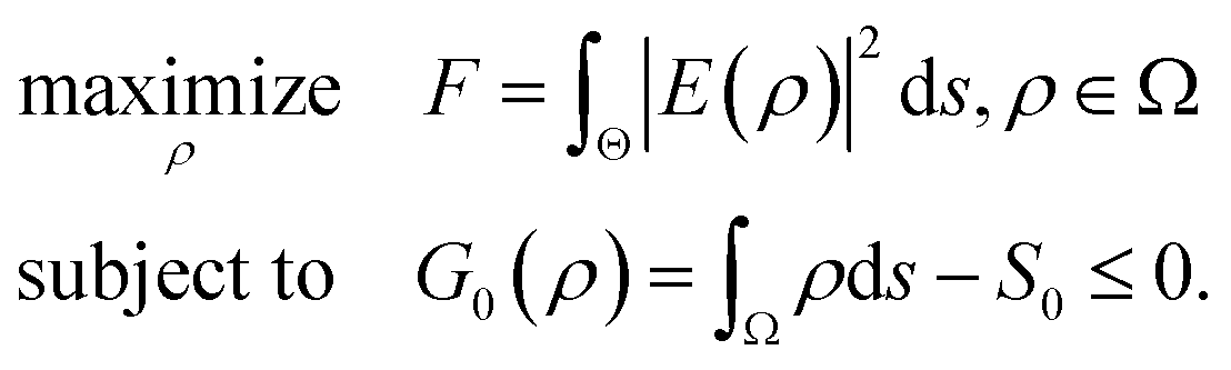
For the majority of PNJ generators, the excitations, e.g., plane waves or Gaussian beams, are free-space propagating waves. Although propagating waves can generate the sub-diffraction-limit waist of some PNJs, excitation via non-conventional sources can produce interesting features of the localized field. Specifically, it has been reported that a PNJ can be excited by surface plasmon polaritons (SPPs) at the shadow-side surfaces of dielectric microdisks positioned on gold films.120 The SPP-assisted PNJ can propagate over several optical wavelengths without sacrificing a subwavelength FWHM. The strong amplitude of the SPPs makes it possible to generate a PNJ with ultra-high field concentration, which shows great promise for enhanced Raman scattering and integrated plasmonic circuits. Similar investigation on SPP-assisted PNJs can be found for 3D dielectric cuboids121 and a cube with a prism.122 The SPP-assisted PNJ generation, theoretically, can be regarded as a phenomenon in two-dimensional systems because the SPPs are confined to the interface of a metal–dielectric composite. However, the short propagation length of SPPs in a planar system notoriously hinders the diverse applications of the proposal of a 2D PNJ. Recently, Kim et al. solved this problem and explored, numerically and experimentally, the use of Bloch surface waves sustained by a suitably structured dielectric media to enable subwavelength focusing in a planar optical system.123 See Fig. 5(a–c). A similar investigation was also implemented by Kim for a two-dimensional fraxicon.124 Augenstein et al. utilized the same experimental configuration as in Kim's work, to focus Bloch surface waves down to a sub-wavelength scale through a pixelized PNJ generator rather than triangles.125 So far, the generation of PNJs is primarily achieved by focusing the central parts of excitation beams (either in 2D or 3D forms), but we should mention that the focusing properties are also governed by the edge diffraction, making it possible to observe tilted PNJs on the edge of a customized dielectric microstructure.126 See the results for a customized microstructure shown in Fig. 5(d). Apparently, the introduction of non-conventional excitation modes adds another dimension to the tuning of PNJs, making it a promising ingredient for a future generation of integrated photonic devices or lab-on-chip devices for specific sensing applications.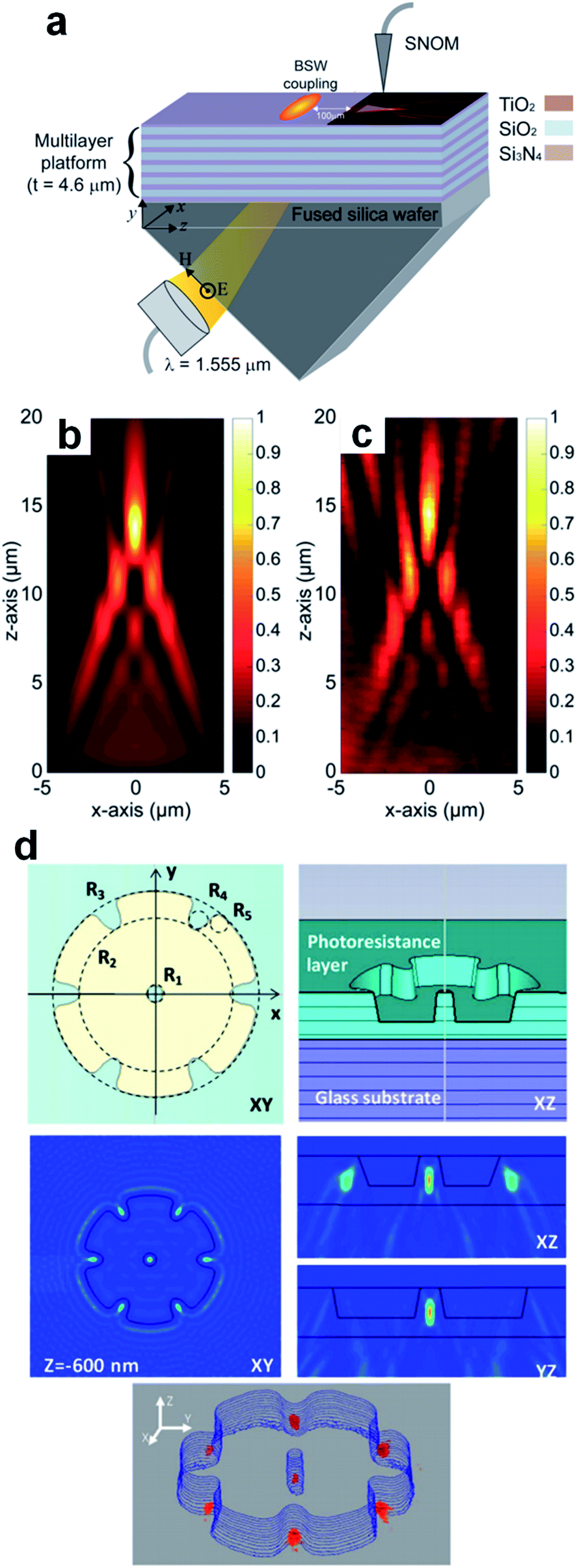 | ||
| Fig. 5 (a) Schematic of the experimental setup including the multilayer structure, Kretschmann coupling configuration, and the scanning nearfield optical microscope probe. (b) Simulated result for the x–z intensity distribution. (c) Measured near-field intensity distribution of the fabricated funnel device. Reproduced with permission from ref. 123. Copyright 2017, American Chemical Society. (d) Near field focusing with a flower-shaped cavity. Reproduced with permission from ref. 126. Copyright 2018, Optical Society of America. | ||
2.6 Generalized design framework for PNJs
The underlying physics of the generation of PNJs, essentially, is the diffraction and interference of light in the volume with dimensions comparable to or larger than the wavelength, which could happen in either the far-field or the near-field. Such an essence indicates that arbitrary-shaped microstructures, with wavelength-scale dimensions, may offer similar functionality as that of the aforementioned PNJ generators.112 The PNJ generators (for instance, microspheres and their derivatives, cuboids, and axicons) as have been reviewed in Sections 2.2–2.4, can be regarded as being obtained from the basic shapes of nature and our physical intuition. However, those conventional shapes and their derivatives only occupy a very limited space of possible PNJ designs. For this reason, we review the generalized framework that could guide the design of PNJ generators with non-conventional shapes, and present preliminary results, to extend current researches and guide future efforts in the field of PNJ design.The key to engineering PNJ generators for specific functionality, without any doubt, is inverse design. It is limiting to attempt to find optimal designs through physical intuition and through secondary developments based on the traditional templates of the standard photonic design library (e.g., spheres, cuboids, and axicons). Hence, we need an inverse design framework that can explore a maximum number of degrees of freedom. For this reason, topology optimization (TO) may be the best choice, because TO is more general than shape optimization or sizing optimization in the sense that the design can attain any shape within the design space, instead of dealing with predefined configurations.127–133 In fact, TO has been utilized extensively in the design of photonic devices, especially in the fields of photonic crystals, waveguides, and bandpass filters.134–143 For the design of PNJs based on TO, the fundamental physics is that each dielectric optimization element (e.g., a mesh element), whose size is much smaller than the excitation wavelength, behaves like an electric dipole with unique orientation, strength, and phase lag.144–149 The coupling among all the optimization elements have a strong impact on each individual dipole, which can be approximately described via the semi-analytical theory of discrete dipole approximation.150–158 It is the coupling among all the fundamental elements that enables us to control the microscale or macroscale performance of photonic devices by playing with the material layouts. Consider now a 2D box (6λ × 5λ) with refractive index n = 2 surrounded by vacuum (n = 1); see Fig. 6(a). Our goal is to concentrate the energy of a 633 nm plane wave that illuminates the bottom side of box, to a region with footprint 1λ × 1.5λ at a fixed distance of 7λ above the box. Without any optimization, the field distribution is primarily dominated by the edge scattering of the box, and no energy concentration is observed [see Fig. 6(a)]. To optimize the box with TO, we can formulate the optimization problem in the form as:
 | (4) |
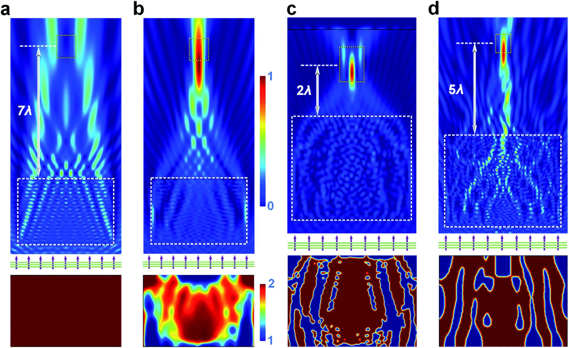 | ||
| Fig. 6 (a) Scattering by a 2D cuboid without optimization. (b) An elongated PNJ generated by a material layout with index spanning the entire range 1–2. Tight PNJs with (c) short and (d) long focal lengths as generated by binary material layouts with different features. | ||
In the density-based TO approach, the design region is meshed and a discretized density variable ρi is assigned on every mesh element (or other fundamental unit). The refractive index at element i in the box is typically calculated using:
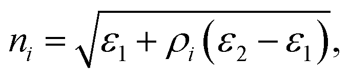 | (5) |
 | (6) |
 | (7) |
 and
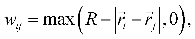
and  are the coordinates of the ith and jth pixels respectively. We should mention that R is a variable specified by users to control the smallest feature size in the optimization, i.e., smaller R generally results in smaller feature sizes in the final material layout. The standard density filter shown in eqn (6) does not prevent grayscale (i.e., intermediate densities). Even with penalization schemes, grayscale features are introduced in a transition region between the different materials. The standard density filter acts as a base upon which other filters are built (e.g., projection filters). Several filters based on Heaviside projections have been proposed in the literature in order to achieve discrete designs and minimum length scales on one or all materials.161 Here, we use a modified form of the approximated Heaviside function projection to process the density variable. The approximated Heaviside function is given as162
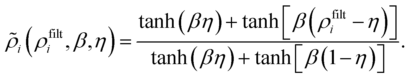 | (8) |
![[small rho, Greek, tilde]](https://www.rsc.org/images/entities/i_char_e0e4.gif) i is the final density variable used in the optimization eqn (4).
i is the final density variable used in the optimization eqn (4).
We now implement the optimization to design a PNJ generator with tight FWHM and elongated length. The bottom of Fig. 6(b) shows an intermediate material layout before the final binary output. In the top of Fig. 6(b), we can clearly find an elongated PNJ generated on the back side of the optimized box. The material (refractive index) distribution in the box is not binary but rather spans the entire range 1–2. As the optimization begins to converge to the maximum of the objection function F, β increases constantly so that the final output of the optimization goes towards a binary layout.
Next, we optimize the design to focus at different distances from the lens. Fig. 6(c) presents an optimized result that behaves like a nearfield lens with a short focal length around 2λ. The controlling variable R is preset as 0.15λ, indicating many small features in the optimized box. See the binary material layout at the bottom of Fig. 6(c). To make the design compatible with state-of-the-art top-down fabrication techniques, we can enlarge R so that small features can be avoided in the final output. Fig. 6(d) presents another design of a lens with a relatively large focal length around (5λ) that corresponds to R = 1.1λ. By comparing with the one shown in Fig. 6(c), we can clearly observe that the material layout in Fig. 6(d) has much larger features and the material distribution is much more uniform, making the real fabrication of the planar devices more feasible. A large R results in a fabricable device, but it sacrifices many degrees of freedom during optimization. Therefore, one has to make a trade-off for the specific application.
To further improve the fabricability, a specific case of TO has been developed by using fundamental geometries like cylinders and cuboids,163 rather than the mesh elements, as the building blocks to design photonic devices.164 Selecting the fundamental unit to be a cuboidal voxel whose size is independent of the mesh is preferable because the mesh can be refined as needed for accurate simulation without affecting the size of the features generated and thus the manufacturability. As one of the demonstrations, Augenstein et al. utilize the cuboid-based inverse photonic design strategy to attain functional elements that focus Bloch surface waves efficiently into spatial domains slightly smaller than half the wavelength.125 They validated the devices by measuring the field distributions with a scanning near-field optical microscope. See Fig. 7(a and b) for the schematic and simulated PNJs. These specific cases of TO are seamlessly compatible with top-down fabrication techniques like dry-etching and FIB, and they enable the design of PNJs with specific performance features (including focal length, working distance, NA, sub-diffraction FWHM, and field enhancement) that cannot be achieved by conventional PNJ generators as aforementioned; thus, we anticipate, TO will be applied extensively in the area of PNJ in the near future.
 | ||
| Fig. 7 (a) Schematic of the experimental scheme (left) and a representative pattern of a relevant functional element (right). (b) Optimization of different structures that can focus Bloch surface waves behind the functional element. The optimized structures are shown in yellow. Reproduced with permission from ref. 125. Copyright 2018, Nature Publishing Group. | ||
We should emphasize at the end of this section that each of the aforementioned PNJ engineering techniques (including index engineering, geometry engineering, non-conventional designs of PNJs, and the generalized design framework for PNJs) enable the customization of all the features of PNJs such as the FWHM, working distance, concentration of electromagnetic energy, and gradient fields. Therefore, they are the basis to the diverse applications of PNJs because a specific application of PNJ is built upon one or several features of PNJs. For this reason, we categorize the diverse applications in the following section according to the application of specific features of PNJs.
3. Diversity in the applications of PNJs
PNJs have many extraordinary properties such as deep-subwavelength FWHM, hot spot with intensive electromagnetic energy, gradient field distribution, backscattering enhancement, and microlensing and resonance effects. The aforementioned PNJ engineering techniques pave the way to customize these features of PNJs and thus may catalyze diverse applications. In the past decade, we have witnessed a bloom in the application of PNJs in many fields spanning from super-resolution imaging and nanoscale sensing to fluorescence enhancement and optical manipulation. We therefore try our best to give a comprehensive review on the emerging fields by categorizing them in terms of the aforementioned properties of PNJs. Among all the applications, it is not surprising that the ones utilizing the feature of high-energy concentration of PNJs dominates, because the high energy-to-volume ratio is the most straightforward advantage of dielectric PNJ generators (especially microspheres). The highly concentrated electromagnetic energy may even trigger the nonlinear effect in materials and thus expands the territory of PNJs to the more universal light–matter interactions for enhancing the existing nonlinear photonic devices. The other properties of PNJs such as gradient field distribution and microlensing effect may facilitate the creation of novel photonic devices such as biophotonic waveguides and spherical photonic crystals. We believe that PNJs will demonstrate their value in more and more exciting fields.3.1 Deep-subwavelength FWHM and nearfield effect of PNJs
It has been extensively reported that PNJs generated by dielectric microspheres can be subdiffraction-limited. A very recent study even showed that the FWHM through material engineering methods can reach λ/7.3.165 This opens new possibilities in a variety of research areas. Moreover, if the narrow PNJ generated by a PNJ generator (for instance, microspheres) is in close contact with a sample surface, a local field enhancement in the area between the bottom of the generator and the sample surface may be established, making the light-matter-interaction occur in an unconventional manner. Super-resolution imaging, nanofabrication beyond diffraction limit, and high-density optical data storage are representative examples that to some extent benefit from the subdiffraction-limited waist of PNJs and nearfield effect.166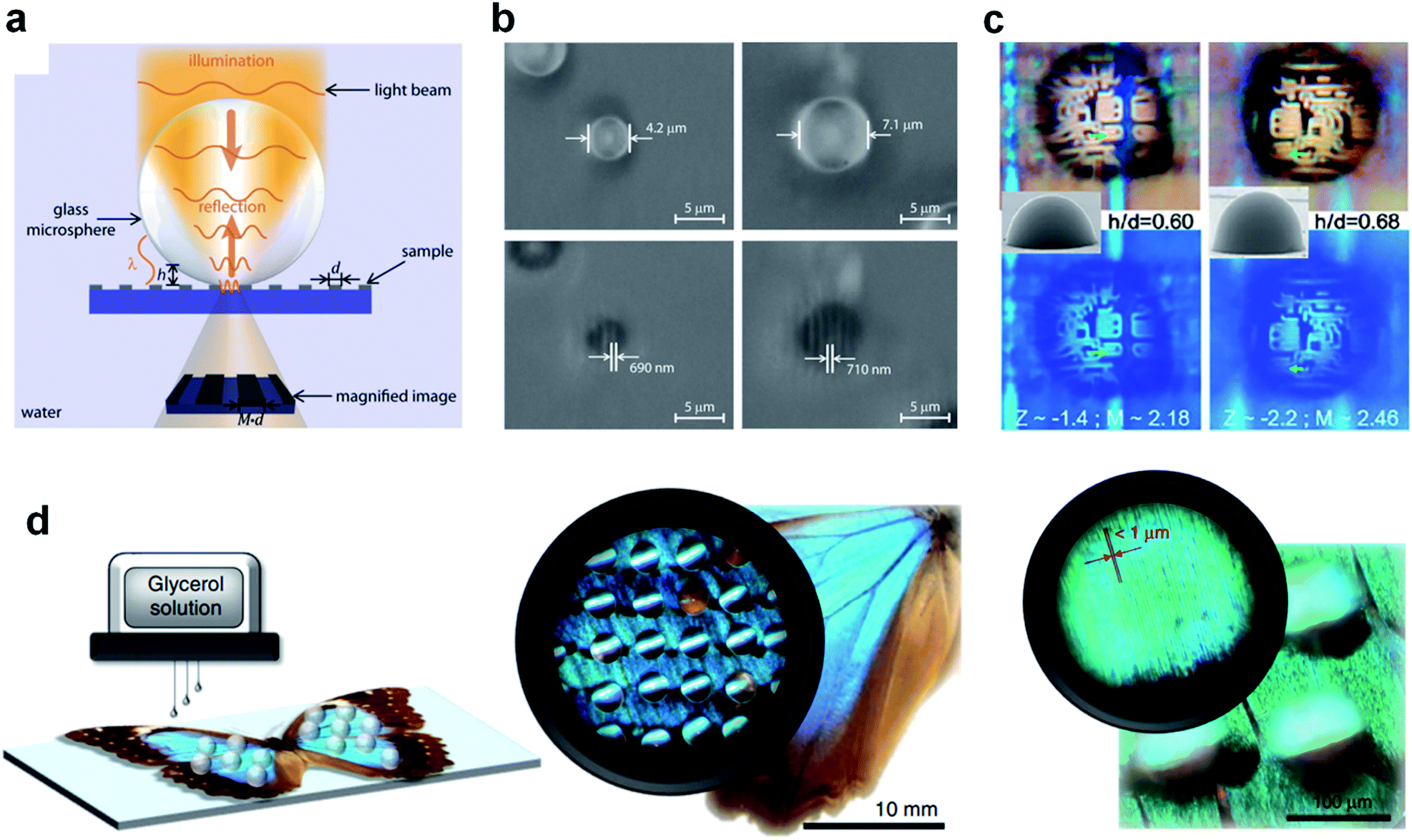 | ||
| Fig. 8 (a) Schematic of the microsphere-based super-resolution imaging process. (b) Optical microscope images of the nanolenses on patterned substrates. Reproduced with permission from ref. 31. Copyright 2016, American Chemical Society. (c) Super-resolution imaging for microelectronics using hSILs with various lens curvatures. Reproduced with permission from ref. 176. Copyright 2016, American Chemical Society. (d) In situ printing of glycerol superlenses for the super-resolution imaging of nanostructures on butterfly wings. Reproduced with permission from ref. 179. Copyright 2019, Nature Publishing Group. | ||
Different than other super-resolution imaging techniques like hyperlens and superlens,189–191 super-oscillation lens,17,192–194 and fluorescence-based modalities,195,196 the underlying physics of imaging beyond the Rayleigh limit via dielectric microspheres has not been completely revealed yet, although there was a study that claimed that it is due to the FWHM of PNJs.31 Maslov et al. investigated the theoretical limits of resolution available in microsphere-based nanoscopy using incoherent point emitters in the air.197 Zhou et al. investigated the effects of immersion depth on super-resolution properties of microsphere-assisted nanoimaging with different indices.198 Li et al. investigated the unusual imaging properties of superresolution microspheres by comparing their results with the output of many proposed theories.199 Yang et al. experimentally validated that shrinking the waist of the PNJ of a dielectric microsphere results in higher lateral resolution.31 Duan et al. theoretically modelled the imaging process through a microlens with vectorial electromagnetic analysis, and then excluded the previously plausible explanation of super-resolution based on the super-focusing effect.200 All the preliminary results show that, the sub-100 nm imaging resolution achieved by a microsphere with a perfect spherical shape need more physical investigation. In fact, the contact imaging mode in microsphere-assisted nanoscopy facilitates the interaction between microspheres and the evanescent components of the excited objects. The tunneling of evanescent waves into propagating waves and the transmission enhancement in the conversion,27 akin to the scanning nearfield optical microscopes,201 may be a potential direction for further investigations on the underlying physics of microsphere nanoscopy.
It is apparent that the random distribution of microspheres prohibits the controllable fabrication of desired structures. Diverse methods, including self-assembly,215–217 off-axis irradiation,218 tweezing (either optical or mechanical),219 and micro-lens arrays,220 have been developed, to manipulate individual microspheres or microsphere arrays for fabricating customized patterns. The 3D coherent nanolithography process that utilizes the focal spots generated by a self-assembled periodic nanosphere array has been successfully developed in recent years. The Talbot field then exposes a pattern onto the underlying photoresist, recording the 3D intensity distribution. Nanostructures with feature size down to one-fourth of the operating wavelength were achieved.221 See the schematic of the principle and experimental results in Fig. 9(a). A natural extension is that arbitrary periodic nanostructures with optimized topography can be utilized to create 3D patterns in photoresists.222–226 Although the self-assembly method makes it possible to pattern over a large area, it is primarily used to fabricate nanoholes. Off-axis irradiation can be combined with the self-assembly method to fabricate arbitrary structure patterns.170 The key for the off-axis irradiation method is varying both the illumination intensity and the illumination angle of the beam impinging on the microspheres such that both the strength and the position of the PNJs generated on the back side can be tuned. Li et al. used a self-assembled particle lens array with near-field enhancement effect to write millions of nano-sized user-defined features through off-axis irradiation.218 They demonstrated that about a 5 mm × 5 mm area can be written with a single shot of a laser beam or a few scans for up to 100 million identical features of nano or sub-micro scales. Compared to the off-axis irradiation and self-assembly based nanopatterning, the utilization of either optical tweezers or mechanical cantilevers to hold microspheres can facilitate the fabrication of more uniform nanostructures.227 This is especially the case when the microsphere is embedded in an atomic force microscopy (AFM) cantilever because the precise control of the AFM cantilever translates into precise positioning and movement of the generated PNJs.228,229 See the cantilever-based nanolithography in Fig. 9(b). To further improve the throughput without sacrificing the positioning accuracy and pattern uniformity, one can embed multiple microspheres into a controllable stage so that it behaves like a microlens array. By properly choosing the illumination wavelength and the size of microspheres, the properties of PNJs can be customized to rapidly pattern superficial and 3D structure arrays.230 A more easy-to-implement method to achieve controllable nanofabrication is varying the properties of illumination sources. This is because the properties of PNJs are sensitive to the illumination conditions [e.g., polarization, phase (if multi-beam illumination is introduced), and angles]. See Fig. 9(c) showing the fabricated nanostructures as functions of polarization states.231,232 We recommend ref. 228 to our readers for more information regarding microsphere-based nanofabrication.
 | ||
| Fig. 9 (a) Schematic of PNJ-assisted 3D nanofabrication using nanospheres. A hexagonal array of nanospheres is illuminated by a UV laser to generate a 3D intensity distribution. The experimental results on the left side are the micrographs obtained for different layers. Reproduced with permission from ref. 221. Copyright 2011, American Chemical Society. (b) Schematic illustration and SEM image of a cantilever with a bead placed inside the circular rim. The right SEM images are the fabricated 2D nanostructures. Reproduced with permission from ref. 229. Copyright 2017, American Chemical Society. (c) Fabricated hollow 3D nanostructures using TE- and TM-polarized illuminations. Reproduced with permission from ref. 231. Copyright 2013, American Chemical Society. | ||
3.2 Concentration of electromagnetic energy
From angular spectrum theory, the generation of PNJs indicates that there is wavefront modulation and constructive interference of different angular components. If the phase of most components are properly tailored, constructive interference can be maximized, leading to a hot spot with intense electromagnetic energy density. Such a high-energy PNJ can significantly enhance the performance of many existing devices and even trigger nonlinear effect in materials. A dielectric microsphere, which has a very high energy-collection-to-volume ratio, is a nearly ideal PNJ generator that has been used extensively in fields such as enhanced Raman scattering, enhanced second harmonic generation from monolayer materials, and optical surgery. Therefore, we will give a review for the emerging fields that are primarily built upon the high-energy concentration feature of PNJs.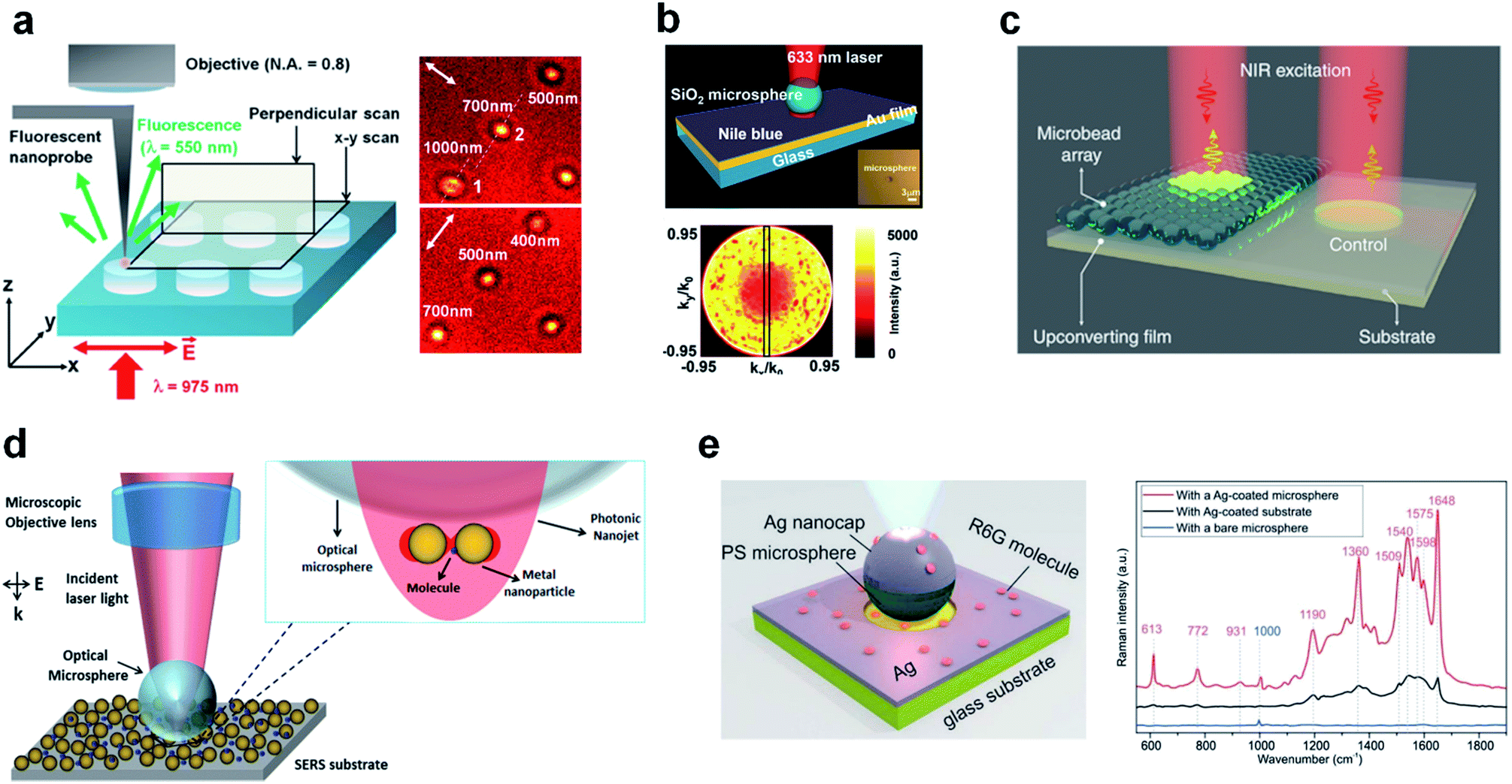 | ||
| Fig. 10 (a) Schematic diagram showing the illumination configuration of the fluorescence scanning near-field optical microscopy, and representative experimental results. Reproduced with permission from ref. 242. Copyright 2017, American Institute of Physics. (b) Schematic of a system consisting of a metal film coupled to a SiO2 micro-resonator, and the Fourier space image captured from a microsphere that is coupled to a Nile blue coated glass substrate. Reproduced with permission from ref. 243. Copyright 2018, John Wiley & Sons, Inc. (c) Schematic illustration of an experimental setup designed for luminescence amplification. Reproduced with permission from ref. 246. Copyright 2019, Nature Publishing Group. (d) Schematic of the PNJ-based Raman scattering enhancement mechanism, and an optical image showing a microsphere excited by a laser. Reproduced with permission from ref. 252. Copyright 2016, American Institute of Physics. (e) Schematic showing enhanced Raman scattering using an Ag-coated dielectric microsphere scheme, and the measured Raman spectra for R6G on an Ag-coated glass substrate. Reproduced with permission from ref. 259. Copyright 2019, John Wiley & Sons, Inc. | ||
Dielectric microspheres have enhanced the Raman scattering signal by up to 1020 or more in perfectly smooth spherical resonators using WGMs.250 It is known that evanescent waves that propagate tangent to the sphere's surface and can extend outward for several hundreds of nanometers.251 Thus, any molecule adsorbed onto the sphere's surface can be interrogated many times by the circulating photons;252,253 thus, microspheres with sizes of r ≫ λ are potentially powerful tools for the label-free sensing of surface analytes.254 However, the resonance feature of microspheres is not the only mechanism for Raman scattering enhancement. PNJs induced by microspheres with sizes in the range of 2–40λ can achieve similar results because the light in the PNJ can be concentrated into a volume that is one order of magnitude smaller than that for conventional focusing lenses. Yi et al. used a narrow PNJ (i.e., a waist of 120 nm and a height of 100 nm) to enhance the Raman peaks of silicon.255 Alessandri et al. utilized similar SiO2 microspheres as versatile, universal Raman scattering enhancers. They demonstrated that the detection limits can be improved by several orders of magnitude, for different substrates consisting of diverse materials.256 The PNJ-based Raman scattering enhancement, generally, can be illustrated by a laser-excited microsphere positioned in an environment of surface analytes.257 See the schematic and a laser-excited microsphere in Fig. 10(d).258 This can be regarded as the foundation of other PNJ-based Raman scattering enhancement mechanisms. For instance, the Raman signal from metal-coated dielectric microspheres interacting with 10−6 M Rhodamine 6G molecules, as measured on the microsphere's top surface, is up to seven times larger than that measured from a flat silver film. An enhancement factor of up to 108 is estimated compared with the case of a non-plasmonic microsphere surface. See the schematic and the measured Raman signal for R6G in Fig. 10(e).259 The combination of metal and dielectrics, as well as doped semiconductors (so that Joule heating can be controlled without sacrificing the dielectric properties), opens up new possibilities for the PNJ-based Raman scattering enhancement.
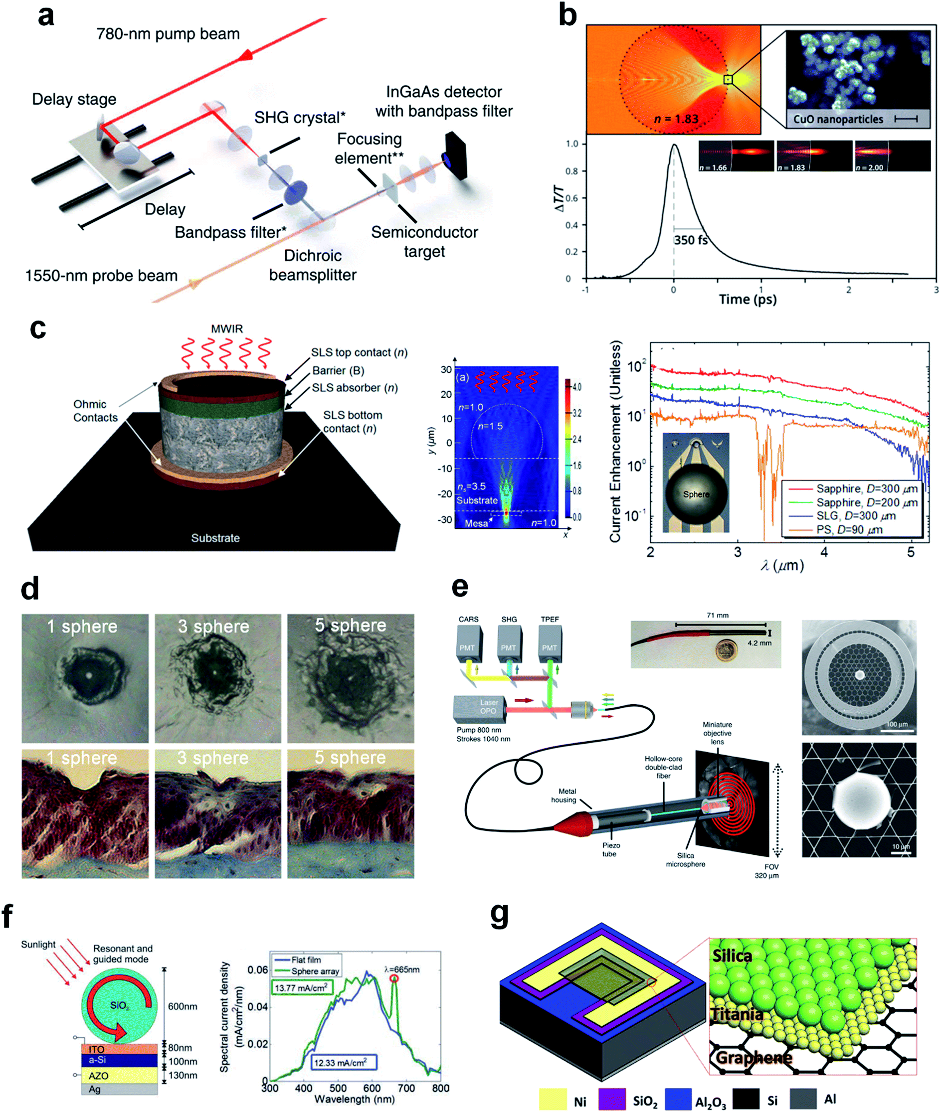 | ||
| Fig. 11 (a) Schematic of the pump–probe experimental set-up. A 780 nm pump beam is used for the GaAs and Si targets and a 390 nm pump beam is used for the SiC target. Reproduced with permission from ref. 261. Copyright 2015, Nature Publishing Group. (b) Normalized differential transmission of the signal beam, ΔT/T, is shown versus time for CuO particles. The inset shows the focusing property of microspheres. Reproduced with permission from ref. 262. Copyright 2016, American Chemical Society. (c) Schematic of a mid-wave infrared detector, the simulated field distribution for a PNJ-assisted photodetector, and photocurrent enhancement factors. Reproduced with permission from ref. 265. Copyright 2016, American Institute of Physics. (d) Representative bird's eye corneal crater images and histology images for one-, three-, and five-sphere probes at 0.1 mJ. Reproduced with permission from ref. 268. Copyright 2012, Society of Photographic Instrumentation Engineers. (e) Schematic of the coherent Raman endoscope and SEM images of microsphere lens inserted into the hollow fiber core. Reproduced with permission from ref. 269. Copyright 2018, Nature Publishing Group. (f) Schematic and spectral current curves of the WGMs-assisted solar cell system. Reproduced with permission from ref. 277. Copyright 2011, John Wiley & Sons, Inc. (g) Schematic of leaf-inspired graphene/Si solar cell with a bilayer configuration of silica/titania nanoparticles on graphene. Reproduced with permission from ref. 284. Copyright 2019, Elsevier. | ||
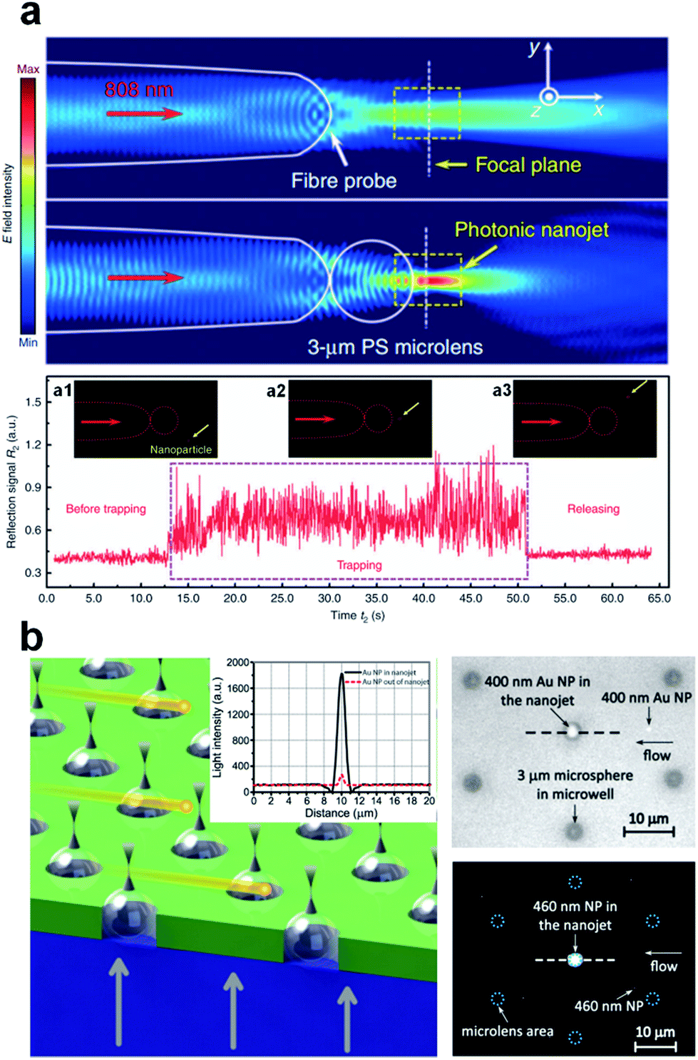 | ||
| Fig. 12 (a) The real-time trace of the reflected 808 nm signal in the trapping process of an 85 nm fluorescent nanoparticle, and optical images showing the dynamic trapping of nanoparticles and plasmid DNA molecules. The insets in the bottom sub-figure of (a) show the fluorescent images (a1) before trapping, (a2) during trapping, and (a3) in the release. Reproduced with permission from ref. 296. Copyright 2016, Nature Publishing Group. (b) Schematic illustration of the optical detection of nanoparticles, and optical images showing the detected nanoparticles by the PNJ array. Reproduced with permission from ref. 298. Copyright 2015, American Chemical Society. | ||
3.3 Gradient field in PNJs
What accompanies a narrow PNJ is a fast divergence of angular components, leading to an intense gradient field. Thus, a strong trapping potential can form around the hot spot, making the manipulation of nanoscale and microscale objects feasible in a sub-wavelength volume. Different from conventional optical tweezers that are diffraction-limited, the ultra-narrow PNJs and resonance feature of microspheres may lead to unique trapping stiffnesses and efficiencies. Stable self-bonding and self-ordering is thus feasible even for biomaterials such as cells and viruses. The tunable parameters of PNJs (e.g., FWHM, length, and working distance) even make in vivo manipulation of objects possible. For all these reasons, a comprehensive review on PNJ-based optical manipulation is vital.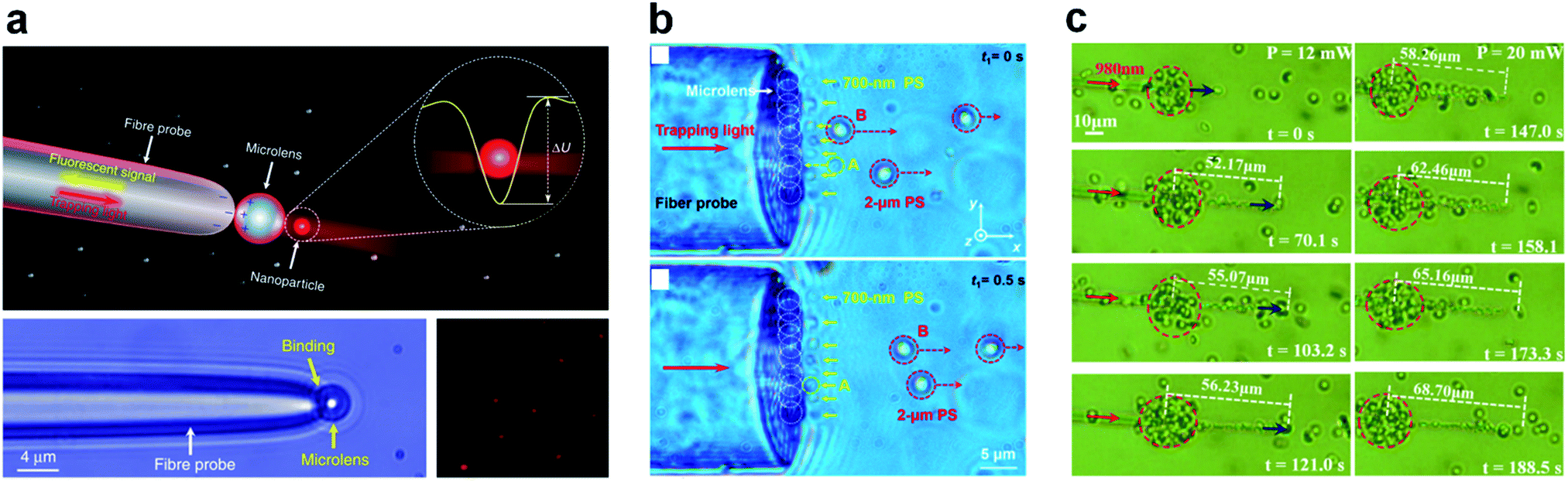 | ||
| Fig. 13 (a) Schematic and experimental optical images of the microlens-based optical manipulation system. Reproduced with permission from ref. 296. Copyright 2016, Nature Publishing Group. (b) Selective trapping of polystyrene (PS) nanoparticles from a mixture of 700 nm and 2 μm PS particles. Reproduced with permission from ref. 305. Copyright 2016, American Chemical Society. (c) Erythrocyte trapping and arrangement processes at different instances of time as the incident power increases to 12 mW and 20 mW, respectively. Reproduced with permission from ref. 306. Copyright 2018, Optical Society of America. | ||
3.4 Microlensing, resonance, and self-bonding effects
A dielectric microsphere can be regarded as a microlens under the excitation of a plane wave. A cascade of microspheres with tailored indices, dimensions, and positions can behave as an optical imaging system consisting of multiple 4F components. Electromagnetic energy thus propagates through such a cascaded system in a periodically “convergence–divergence” manner. The resonance feature of microspheres can also enable low-loss waveguiding effects and even sharp bending for a cascade of contacted microspheres. Self-bonding that originates from trapping potential of PNJs enables the automatic formation of waveguides in liquid environments. We now review emerging applications of PNJ-based waveguides.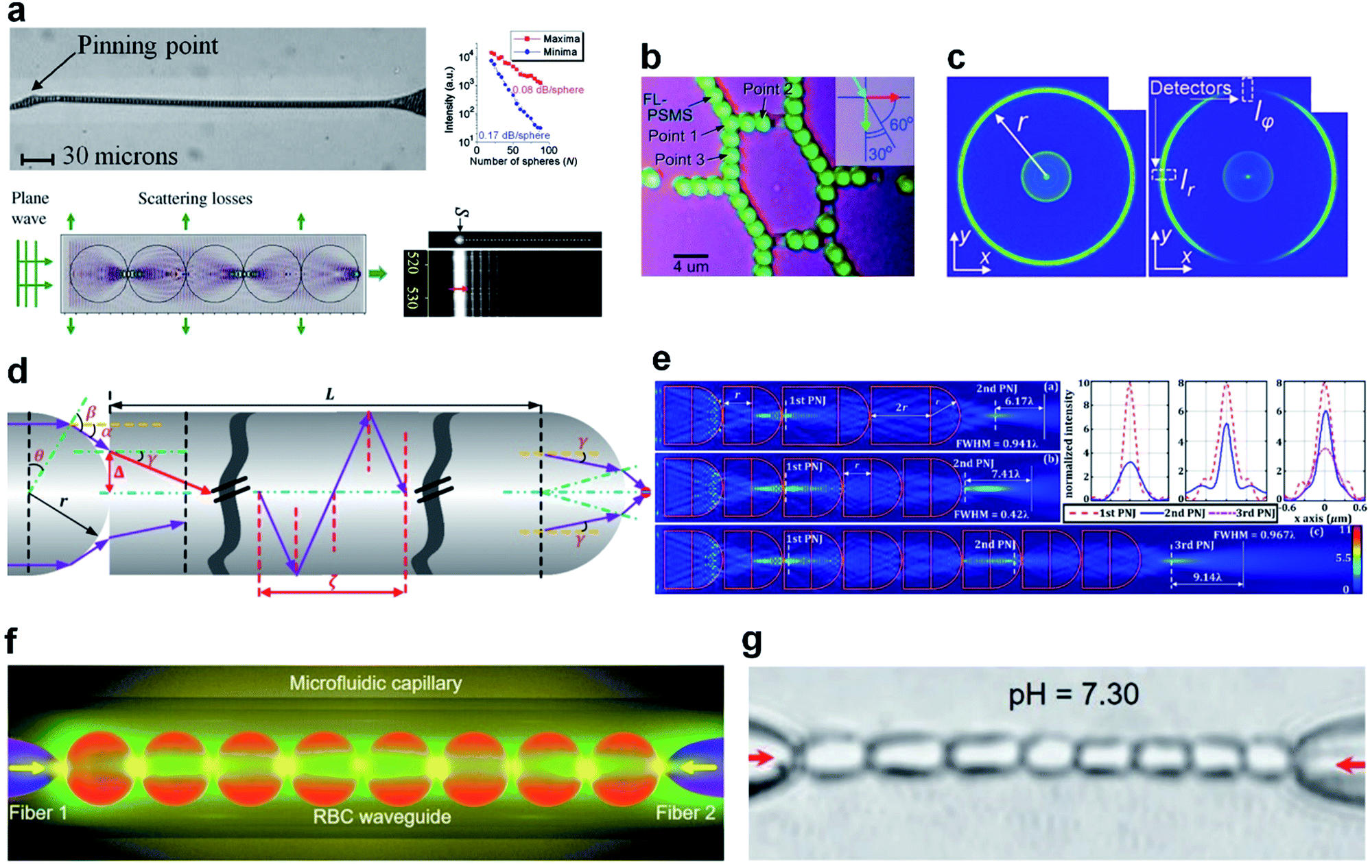 | ||
| Fig. 14 (a) Optical image of a chain consisting of 5.0 μm microspheres, and representative numerical and experimental figures for a waveguide chain. Reproduced with permission from ref. 319. Copyright 2008, American Institute of Physics. (b) Optical microscope image of microsphere coupled-resonator optical waveguides with branched structures. Reproduced with permission from ref. 322. Copyright 2010, John Wiley & Sons, Inc. (c) Cross-section intensity distribution obtained at the end of a chain of 20 spheres with n = 1.71 as a result of illumination with collimated rays, and cross-section intensity distribution with the polarizer installed also showing positions of two detectors (dashed rectangles) used for degree-of-freedom calculations. Reproduced with permission from ref. 324. Copyright 2013, Optical Society of America. (d) Illustrated diagram showing the effect of the length L and hemispherical radius r on the focus property and (e) spatial intensity distribution maps showing the effect of length L and number of cascaded elements on the optical transport, and comparisons of the PNJ hot-spot cross-sectional profiles corresponding to the right-hand side sub-figures. Reproduced with permission from ref. 92. Copyright 2016, Optical Society of America. (f and g) Schematic and real optical images of the cell waveguide generated by two fiber probes in a microfluidic capillary. Reproduced with permission from ref. 326. Copyright 2019, John Wiley & Sons, Inc. | ||
Conclusions and outlook
This article reviewed many recent developments in the design of PNJ generators as well as the diverse applications based on PNJs. The conventional approaches to engineer the properties of PNJs, including the index- and geometry-based ones, have been thoroughly discussed and the dynamically controllable PNJ generation mechanisms, although rarely investigated, have been highlighted to remind readers of their importance. Natural materials that behave as PNJ generators have been discussed to enlighten future exploration in bio-inspired nanotechnology. Novel principles and frameworks, including the focusing for Bloch surface waves and plasmonic resonances as well as the pixel-based and density-based general inverse design mechanisms, have expanded the territory of PNJs tremendously. For a dielectric material with an arbitrary refractive index, researchers can now easily design ultra-narrow, elongated, highly concentrated, multiple, or any other types of PNJs. Therefore, we personally forecast two potentially important topics relating to the design of PNJs. The first is the dynamic tuning of PNJs for diverse applications via mechanisms like controllable liquid crystal molecules. The dynamic range of index or geometry control determines the tuning range of the generated PNJs. Thus, we believe this dynamic range should be treated as a significant benchmark when exploring new physical mechanisms for generating PNJs. The second is the generalized frameworks for inverse PNJ design. The vast degrees of freedom in these design frameworks together with 3D fabrication techniques such as grayscale lithography facilitate the generation of diverse PNJs beyond the conventional limitations such as n < 2 and beyond the standard geometries such as spheres and cuboids.The scientific and engineering applications of PNJs are even more exciting. We have witnessed a bloom arising from the use of PNJs across diverse disciplines. The highly concentrated energy in PNJs may catalyze the re-examination of light–matter interactions, but the unique resonant and mode features in standard geometries like spheres and cylinders, are also responsible for the prosperity. Optical nanoscopy, nanoscale fabrication, optical data storage, enhanced Raman scattering, waveguide chains, and enhanced sensing, are conventionally understandable areas where PNJs contribute significantly, but recent works by multiple research groups and the introduction of non-spherical schemes have pushed those areas to an even higher level. The imaging limit of microsphere-assisted nanoscopy is still being pushed forward; the nanopatterning has been expanded from 2D to 3D; up to 0.08 dB loss per sphere has been experimentally demonstrated in a microsphere chain; and several orders of magnitude enhancement in Raman scattering and sensing have been observed in both resonance and non-resonance modes. The extension to other areas like laser surgery and optical manipulation, offers the possibility of combing PNJs with conventional instruments like Mueller matrix polarimeters and optical tweezers, to enable the enhanced performance as well as the new working modalities. The combination of multiple features of PNJs enables multifunctional devices such as the one combining gradient field and enhanced backscattering for achieving self-bonding of cells and dynamic sensing of nanoparticles in the same microchamber. We have noticed an important trend that PNJs are becoming critical in several areas that are dominated by nonlinear optics, such as all-optical switching and laser machining. We believe the applications of PNJs in nonlinear optics will keep growing as it has in linear optics. At the end, we should emphasize that the generalized inverse PNJ design mechanisms as well as bio-inspired PNJs will undoubtedly contribute to the diverse applications of PNJs in terms of manufacturability, compatibility, and generalizability, which are critical to many fields such as semiconductors, photonics, and biomedicine.
Conflicts of interest
There are no conflicts to declare.Acknowledgements
This work was funded by Cisco Systems Inc. (gift awards CG 1141107 and CG 1377144), University of Illinois at Urbana-Champaign College of Engineering Strategic Research Initiative, and Zhejiang University – University of Illinois at Urbana-Champaign (ZJUI) Institute Research Program. We acknowledge Cisco System Inc. for access to its Arcetri cluster. L. L. G. acknowledges the Center for Advanced Study at the University of Illinois for teaching release time.Notes and references
- D. K. Gramotnev and S. I. Bozhevolnyi, Nat. Photonics, 2010, 4, 83–91 CrossRef CAS.
- J. B. Khurgin, Nat. Nanotechnol., 2015, 10, 2–6 CrossRef CAS PubMed.
- D. R. Smith, J. B. Pendry, M. C. K. Wiltshire and X. Zhang, Science, 2004, 305, 788–792 CrossRef CAS PubMed.
- J. N. Anker, W. P. Hall, O. Lyandres, N. C. Shah, J. Zhao and R. P. Van Duyne, Nat. Mater., 2008, 7, 442–453 CrossRef CAS PubMed.
- A. G. Brolo, Nat. Photonics, 2012, 6, 709–713 CrossRef CAS.
- T. Harter, S. Muehlbrandt, S. Ummethala, A. Schmid, S. Nellen, L. Hahn, W. Freude and C. Koos, Nat. Photonics, 2018, 12, 625–633 CrossRef CAS.
- M. Schnell, P. Alonso-González, L. Arzubiaga, F. Casanova, L. E. Hueso, A. Chuvilin and R. Hillenbrand, Nat. Photonics, 2011, 5, 283–287 CrossRef CAS.
- H. Choo, M. K. Kim, M. Staffaroni, T. J. Seok, J. Bokor, S. Cabrini, P. J. Schuck, M. C. Wu and E. Yablonovitch, Nat. Photonics, 2012, 6, 838–844 CrossRef CAS.
- H. Im, H. Shao, Y. Il Park, V. M. Peterson, C. M. Castro, R. Weissleder and H. Lee, Nat. Biotechnol., 2014, 32, 490–495 CrossRef CAS PubMed.
- Z. Liu, S. Durant, H. Lee, Y. Pikus, N. Fang, Y. Xiong, C. Sun and X. Zhang, Nano Lett., 2007, 7, 403–408 CrossRef CAS PubMed.
- S. Law, L. Yu, A. Rosenberg and D. Wasserman, Nano Lett., 2013, 13, 4569–4574 CrossRef CAS PubMed.
- F. Yesilkoy, E. R. Arvelo, Y. Jahani, M. Liu, A. Tittl, V. Cevher, Y. Kivshar and H. Altug, Nat. Photonics, 2019, 13, 390–396 CrossRef CAS.
- Y. T. Kim, H. Min, J. Lee, H. Park and C. Y. Lee, Nanoscale, 2018, 10, 1030–1037 RSC.
- P. Albella, M. A. Poyli, M. K. Schmidt, S. A. Maier, F. Moreno, J. J. Sáenz and J. Aizpurua, J. Phys. Chem. C, 2013, 117, 13573–13584 CrossRef CAS.
- M. R. Shcherbakov, P. P. Vabishchevich, A. S. Shorokhov, K. E. Chong, D.-Y. Choi, I. Staude, A. E. Miroshnichenko, D. N. Neshev, A. A. Fedyanin and Y. S. Kivshar, Nano Lett., 2015, 15, 6985–6990 CrossRef PubMed.
- R. Regmi, J. Berthelot, P. M. Winkler, M. Mivelle, J. Proust, F. Bedu, I. Ozerov, T. Begou, J. Lumeau, H. Rigneault, M. F. García-Parajó, S. Bidault, J. Wenger and N. Bonod, Nano Lett., 2016, 16, 5143–5151 CrossRef CAS PubMed.
- N. I. Zheludev, Nat. Mater., 2008, 7, 420–422 CrossRef CAS PubMed.
- G. Chen, Y. Li, X. Wang, Z. Wen, F. Lin, L. Dai, L. Chen, Y. He and S. Liu, IEEE Photonics Technol. Lett., 2016, 28, 335–338 CAS.
- A. M. H. Wong and G. V. Eleftheriades, Sci. Rep., 2015, 5, 1–6 Search PubMed.
- V. R. Almeida, Q. Xu, C. A. Barrios and M. Lipson, Opt. Lett., 2004, 29, 1209 CrossRef PubMed.
- Q. Xu, V. R. Almeida, R. R. Panepucci and M. Lipson, Opt. Lett., 2004, 29, 1626 CrossRef CAS PubMed.
- B. S. Luk'yanchuk, R. Paniagua-Domínguez, I. Minin, O. Minin and Z. Wang, Opt. Mater. Express, 2017, 7, 1820 CrossRef.
- A. V. Itagi and W. A. Challener, J. Opt. Soc. Am. A, 2005, 22, 2847 CrossRef CAS PubMed.
- A. Heifetz, S.-C. Kong, A. V. Sahakian, A. Taflove and V. Backman, J. Comput. Theor. Nanosci., 2009, 6, 1979–1992 CrossRef CAS PubMed.
- Q. Li, M. Davanço and K. Srinivasan, Nat. Photonics, 2016, 10, 406–414 CrossRef CAS.
- Z. Wang, W. Guo, L. Li, B. Luk'Yanchuk, A. Khan, Z. Liu, Z. Chen and M. Hong, Nat. Commun., 2011, 2, 216–218 CrossRef PubMed.
- Y. Ben-Aryeh, Appl. Phys. B: Lasers Opt., 2012, 109, 165–170 CrossRef CAS.
- Y. Ben-Aryeh, J. Opt. Soc. Am. A, 2016, 33, 2284 CrossRef CAS PubMed.
- Y. Ben-Aryeh, Appl. Phys. B: Lasers Opt., 2006, 84, 121–124 CrossRef CAS.
- Y. Ben-Aryeh, Appl. Phys. B: Lasers Opt., 2008, 91, 157–165 CrossRef CAS.
- H. Yang, R. Trouillon, G. Huszka and M. A. M. Gijs, Nano Lett., 2016, 16, 4862–4870 CrossRef CAS PubMed.
- H. H. Nguyen Pham, S. Hisatake, I. V. Minin, O. V. Minin and T. Nagatsuma, Appl. Phys. Lett., 2016, 108, 191102 CrossRef.
- I. V. Minin, O. V. Minin, D. S. Ponomarev and I. A. Glinskiy, Ann. Phys., 2018, 530, 1800359 CrossRef.
- Y. E. Geints, O. V. Minin and I. V. Minin, Ann. Phys., 2019, 1900033 CrossRef.
- L. Yue, B. Yan and Z. Wang, Opt. Lett., 2016, 41, 1336 CrossRef PubMed.
- A. Rueda, F. Sedlmeir, M. Kumari, G. Leuchs and H. G. L. Schwefel, Nature, 2019, 568, 378–381 CrossRef CAS PubMed.
- U. Keller, Nature, 2003, 424, 831–838 CrossRef CAS PubMed.
- N. Savage, Nat. Photonics, 2009, 3, 114–115 CrossRef CAS.
- G. Epple, K. S. Kleinbach, T. G. Euser, N. Y. Joly, T. Pfau, P. S. J. Russell and R. Löw, Nat. Commun., 2014, 5, 4132 CrossRef CAS PubMed.
- Z. Chen, A. Taflove and V. Backman, Opt. Express, 2004, 12, 1214 CrossRef PubMed.
- X. Li, Z. Chen, A. Taflove and V. Backman, Opt. Express, 2005, 13, 526 CrossRef PubMed.
- J. Zhu and L. L. Goddard, IEEE Photonics Technol. Lett., 2018, 30, 75–78 CAS.
- A. D. Kiselev and D. O. Plutenko, Phys. Rev. A, 2014, 89, 043803 CrossRef.
- J. A. Gonzaga-Galeana and J. R. Zurita-Sánchez, Journal of Electromagnetic Waves and Applications, 2018, 32, 1106–1125 CrossRef.
- A. V. Itagi and W. A. Challener, J. Opt. Soc. Am. A, 2005, 22, 2847 CrossRef CAS PubMed.
- S. Tadepalli, J. M. Slocik, M. K. Gupta, R. R. Naik and S. Singamaneni, Chem. Rev., 2017, 117, 12705–12763 CrossRef CAS PubMed.
- C. B. Lin, Z.-H. Huang and C.-Y. Liu, Opt. Lett., 2019, 44, 667 CrossRef CAS PubMed.
- J. N. Monks, B. Yan, N. Hawkins, F. Vollrath and Z. Wang, Nano Lett., 2016, 16, 5842–5845 CrossRef CAS PubMed.
- N. Schuergers, T. Lenn, R. Kampmann, M. V. Meissner, T. Esteves, M. Temerinac-Ott, J. G. Korvink, A. R. Lowe, C. W. Mullineaux and A. Wilde, Elife, 2015, 5, e12620 CrossRef PubMed.
- J. Zhu, Y. Liu, X. Yu, R. Zhou, J.-M. Jin and L. L. Goddard, Nano Lett., 2019, 19, 5347–5355 CrossRef CAS PubMed.
- J. Zhu, R. Zhou, L. Zhang, B. Ge, C. Luo and L. L. Goddard, Opt. Express, 2019, 27, 6719 CrossRef CAS PubMed.
- Y. Li, X. Liu and B. Li, Light: Sci. Appl., 2019, 8, 61 CrossRef PubMed.
- Y. Li, X. Liu, X. Yang, H. Lei, Y. Zhang and B. Li, ACS Nano, 2017, 11, 10672–10680 CrossRef CAS PubMed.
- Y. Li, H. Xin, Y. Zhang, H. Lei, T. Zhang, H. Ye, J. J. Saenz, C.-W. Qiu and B. Li, ACS Nano, 2018, 12, 10703–10711 CrossRef CAS PubMed.
- H. Xin, Y. Li, X. Liu and B. Li, Nano Lett., 2013, 13, 3408–3413 CrossRef CAS PubMed.
- X. Liu, Y. Li, X. Xu, Y. Zhang and B. Li, ACS Appl. Bio Mater., 2019, 2, 2889–2895 CrossRef CAS.
- L. Miccio, P. Memmolo, F. Merola, P. A. Netti and P. Ferraro, Nat. Commun., 2015, 6, 6502 CrossRef CAS PubMed.
- S. Wilhelm, ACS Nano, 2017, 11, 10644–10653 CrossRef CAS PubMed.
- G. E. Arnaoutakis and B. S. Richards, Opt. Mater., 2018, 83, 47–54 CrossRef CAS.
- N. Yu, P. Genevet, M. A. Kats, F. Aieta, J. P. Tetienne, F. Capasso and Z. Gaburro, Science, 2011, 334, 333–337 CrossRef CAS PubMed.
- S. Pérez-López, J. M. Fuster, I. V. Minin, O. V. Minin and P. Candelas, Sci. Rep., 2019, 9, 13363 CrossRef PubMed.
- S.-C. Kong, A. Taflove and V. Backman, Opt. Express, 2009, 17, 3722 CrossRef CAS PubMed.
- C. Yan, H. Ding and L. Dai, Chin. Opt. Lett., 2010, 8(7), 706–708 CrossRef.
- Y. E. Geints, A. A. Zemlyanov and E. K. Panina, J. Opt. Soc. Am. B, 2011, 28, 1825 CrossRef CAS.
- Y. Shen, L. V. Wang and J.-T. Shen, Opt. Lett., 2014, 39, 4120 CrossRef PubMed.
- G. Gu, R. Zhou, Z. Chen, H. Xu, G. Cai, Z. Cai and M. Hong, Opt. Lett., 2015, 40, 625 CrossRef PubMed.
- Z. Zhen, Y. Huang, Y. Feng, Y. Shen and Z. Li, Opt. Express, 2019, 27, 9178 CrossRef CAS PubMed.
- X. Mao, Y. Yang, H. Dai, D. Luo, B. Yao and S. Yan, Opt. Express, 2015, 23, 26426 CrossRef CAS PubMed.
- J. P. F. Lagerwall and G. Scalia, Curr. Appl. Phys., 2012, 12, 1387–1412 CrossRef.
- G. H. Brown, J. Electron. Mater., 1973, 2, 403–430 CrossRef CAS.
- H. Kikuchi, M. Yokota, Y. Hisakado, H. Yang and T. Kajiyama, Nat. Mater., 2002, 1, 64–68 CrossRef CAS PubMed.
- R. Narayan, J. E. Kim, J. Y. Kim, K. E. Lee and S. O. Kim, Adv. Mater., 2016, 28, 3045–3068 CrossRef CAS PubMed.
- T. J. White and D. J. Broer, Nat. Mater., 2015, 14, 1087–1098 CrossRef CAS PubMed.
- C.-Y. Liu, Phys. Lett. A, 2014, 378, 229–234 CrossRef CAS.
- T. Matsui and A. Okajima, Jpn. J. Appl. Phys., 2014, 53, 01AE04 CrossRef.
- N. Eti, I. H. Giden, Z. Hayran, B. Rezaei and H. Kurt, J. Mod. Opt., 2017, 64, 1566–1577 CrossRef CAS.
- B. Du, J. Xia, J. Wu, J. Zhao, H. Zhang, B. Du, J. Xia, J. Wu, J. Zhao and H. Zhang, Nanomaterials, 2019, 9, 72 CrossRef PubMed.
- T. Matsui and K. Tsukuda, Opt. Lett., 2017, 42, 4663 CrossRef CAS PubMed.
- B. Gholipour, A. Karvounis, J. Yin, C. Soci, K. F. MacDonald and N. I. Zheludev, NPG Asia Mater., 2018, 10, 533–539 CrossRef CAS.
- C. Lan, H. Ma, M. Wang, Z. Gao, K. Liu, K. Bi, J. Zhou and X. Xin, ACS Appl. Mater. Interfaces, 2019, 11, 14229–14238 CrossRef CAS PubMed.
- W. Aftab, X. Huang, W. Wu, Z. Liang, A. Mahmood and R. Zou, Energy Environ. Sci., 2018, 11, 1392–1424 RSC.
- C. Chen, P. Jost, H. Volker, M. Kaminski, M. Wirtssohn, U. Engelmann, K. Krüger, F. Schlich, C. Schlockermann, R. P. S. M. Lobo and M. Wuttig, Phys. Rev. B, 2017, 95, 094111 CrossRef.
- Y. Yang, C.-T. Li, S. M. Sadeghipour, H. Dieker, M. Wuttig and M. Asheghi, J. Appl. Phys., 2006, 100, 024102 CrossRef.
- J. H. Soh, M. Wu, G. Gu, L. Chen and M. Hong, Appl. Opt., 2016, 55, 3751 CrossRef CAS PubMed.
- V. Kumar, P. K. Goyal, S. Mahendia, R. Gupta, T. Sharma and S. Kumar, Radiat. Eff. Defects Solids, 2011, 166, 109–113 CrossRef CAS.
- Y. Yu, Y. Yu, L. Huang, H. Peng, L. Xiong and L. Cao, Nano Lett., 2017, 17, 3613–3618 CrossRef CAS PubMed.
- D. S. Engstrom, B. Porter, M. Pacios and H. Bhaskaran, J. Mater. Res., 2014, 29, 1792–1816 CrossRef CAS.
- K. Du, I. Wathuthanthri, C.-H. Choi, K. Du, I. Wathuthanthri and C.-H. Choi, Micromachines, 2017, 8, 275 CrossRef PubMed.
- J. A. Liddle and G. M. Gallatin, ACS Nano, 2016, 10, 2995–3014 CrossRef CAS PubMed.
- K. Kang, Y. Cho, K. Yu, K. Kang, Y. Cho and K. J. Yu, Micromachines, 2018, 9, 263 CrossRef PubMed.
- A. Polman and H. A. Atwater, Nat. Mater., 2012, 11, 174–177 CrossRef CAS.
- J. Zhu and L. L. Goddard, Opt. Express, 2016, 24, 30444 CrossRef CAS PubMed.
- M.-S. Kim, T. Scharf, S. Mühlig, C. Rockstuhl and H. P. Herzig, Opt. Express, 2011, 19, 10206 CrossRef PubMed.
- Y. E. Geints, A. A. Zemlyanov and E. K. Panina, Quantum Electron., 2011, 41, 520–525 CrossRef CAS.
- D. Grojo, N. Sandeau, L. Boarino, C. Constantinescu, N. De Leo, M. Laus and K. Sparnacci, Opt. Lett., 2014, 39, 3989 CrossRef PubMed.
- V. Pacheco-Peña and M. Beruete, J. Appl. Phys., 2019, 125, 084104 CrossRef.
- Y. Huang, Z. Zhen, Y. Shen, C. Min and G. Veronis, Opt. Express, 2019, 27, 1310 CrossRef CAS PubMed.
- S. Zhou, Jpn. J. Appl. Phys., 2019, 58, 050920 CrossRef CAS.
- Z. Hengyu, C. Zaichun, C. T. Chong and H. Minghui, Opt. Express, 2015, 23, 6626 CrossRef CAS PubMed.
- D. McCloskey, J. J. Wang and J. F. Donegan, Opt. Express, 2011, 20, 128 CrossRef PubMed.
- M. X. Wu, B. J. Huang, R. Chen, Y. Yang, J. F. Wu, R. Ji, X. D. Chen and M. H. Hong, Opt. Express, 2015, 23, 20096 CrossRef CAS PubMed.
- M. Wu, R. Chen, J. Soh, Y. Shen, L. Jiao, J. Wu, X. Chen, R. Ji and M. Hong, Sci. Rep., 2016, 6, 31637 CrossRef CAS PubMed.
- V. V. Kotlyar, S. S. Stafeev and A. Feldman, Appl. Opt., 2014, 53, 5322 CrossRef PubMed.
- I. V. Minin, O. V. Minin, V. Pacheco-Peña and M. Beruete, Opt. Lett., 2015, 40, 2329 CrossRef CAS PubMed.
- D. McCloskey, K. E. Ballantine, P. R. Eastham and J. F. Donegan, Opt. Express, 2015, 23, 26326 CrossRef CAS PubMed.
- L. Yue, B. Yan, J. N. Monks, Z. Wang, N. T. Tung, V. D. Lam, O. Minin and I. Minin, J. Phys. D: Appl. Phys., 2017, 50, 175102 CrossRef.
- J. Yang, P. Twardowski, P. Gérard, Y. Duo, J. Fontaine and S. Lecler, Opt. Express, 2018, 26, 3723 CrossRef CAS PubMed.
- Y. E. Geints, A. A. Zemlyanov, O. V. Minin and I. V. Minin, J. Opt., 2018, 20, 065606 CrossRef.
- H. H. Nguyen Pham, S. Hisatake, O. V. Minin, T. Nagatsuma and I. V. Minin, Appl. Phys. Lett., 2017, 110, 201105 CrossRef.
- B. Zhang, J. Hao, Z. Shen, H. Wu, K. Zhu, J. Xu and J. Ding, Appl. Opt., 2018, 57, 8331 CrossRef CAS PubMed.
- Y. E. Geints, A. A. Zemlyanov and E. K. Panina, J. Opt. Soc. Am. B, 2015, 32, 1570 CrossRef CAS.
- Y. E. Geints and A. A. Zemlyanov, J. Appl. Phys., 2016, 119, 153101 CrossRef.
- C.-Y. Liu, O. V. Minin and I. V. Minin, Europhys. Lett., 2018, 123, 54003 CrossRef.
- S. A. Degtyarev, A. P. Porfirev and S. N. Khonina, Appl. Opt., 2016, 55, B44 CrossRef CAS PubMed.
- H. Zhang, H. Xia and Y. Zhao, ACS Macro Lett., 2014, 3, 940–943 CrossRef CAS.
- S. S. Walavalkar, A. P. Homyk, M. D. Henry and A. Scherer, J. Appl. Phys., 2010, 107, 124314 CrossRef.
- C. Friese and H. Zappe, J. Microelectromech. Syst., 2008, 17, 11–19 Search PubMed.
- Q. Yan and Y. Zhao, J. Am. Chem. Soc., 2013, 135, 16300–16303 CrossRef CAS PubMed.
- S. Kee, N. Kim, B. Park, B. S. Kim, S. Hong, J.-H. Lee, S. Jeong, A. Kim, S.-Y. Jang and K. Lee, Adv. Mater., 2018, 30, 1703437 CrossRef PubMed.
- D. Ju, H. Pei, Y. Jiang and X. Sun, Appl. Phys. Lett., 2013, 102, 171109 CrossRef.
- V. Pacheco-Peña, I. V. Minin, O. V. Minin and M. Beruete, Ann. Phys., 2016, 528, 684–692 CrossRef.
- I. V. Minin, O. V. Minin, D. S. Ponomarev and I. A. Glinskiy, Ann. Phys., 2018, 530, 1800359 CrossRef.
- M. S. Kim, B. Vosoughi Lahijani, N. Descharmes, J. Straubel, F. Negredo, C. Rockstuhl, M. Häyrinen, M. Kuittinen, M. Roussey and H. P. Herzig, ACS Photonics, 2017, 4, 1477–1483 CrossRef CAS.
- M.-S. Kim, A. Vetter, C. Rockstuhl, B. V. Lahijani, M. Häyrinen, M. Kuittinen, M. Roussey and H. P. Herzig, Commun. Phys., 2018, 1, 63 CrossRef.
- Y. Augenstein, A. Vetter, B. V. Lahijani, H. P. Herzig, C. Rockstuhl and M.-S. Kim, Light: Sci. Appl., 2018, 7, 104 CrossRef PubMed.
- A. Boriskin, V. Drazic, R. Keating, M. Damghanian, O. Shramkova and L. Blondé, Opt. Lett., 2018, 43, 4053 CrossRef CAS.
- M. P. Bendsøe and O. Sigmund, Arch. Appl. Mech., 1999, 69, 635–654 CrossRef.
- O. Sigmund and J. Petersson, Struct. Optim., 1998, 16, 68–75 CrossRef.
- O. Sigmund, Struct. Multidiscip. Optim., 2001, 21, 120–127 CrossRef.
- O. Sigmund, Mech. Struct. Mach., 1997, 25, 493–524 CrossRef.
- O. Sigmund, Int. J. Solids Struct., 1994, 31, 2313–2329 CrossRef.
- C. B. W. Pedersen, T. Buhl and O. Sigmund, Int. J. Numer. Methods Eng., 2001, 50, 2683–2705 CrossRef.
- M. Jansen, G. Lombaert, M. Diehl, B. S. Lazarov, O. Sigmund and M. Schevenels, Struct. Multidiscip. Optim., 2013, 47, 317–333 CrossRef.
- P. I. Borel, A. Harpøth, L. H. Frandsen, M. Kristensen, P. Shi, J. S. Jensen and O. Sigmund, Opt. Express, 2004, 12, 1996 CrossRef CAS.
- O. Sigmund and K. Hougaard, Phys. Rev. Lett., 2008, 100, 153904 CrossRef PubMed.
- J. S. Jensen and O. Sigmund, Appl. Phys. Lett., 2004, 84, 2022–2024 CrossRef CAS.
- F. Wang, J. S. Jensen and O. Sigmund, J. Opt. Soc. Am. B, 2011, 28, 387 CrossRef CAS.
- J. S. Jensen, O. Sigmund, L. H. Frandsen, P. I. Borel, A. Harpoth and M. Kristensen, IEEE Photonics Technol. Lett., 2005, 17, 1202–1204 CAS.
- L. F. Frellsen, Y. Ding, O. Sigmund and L. H. Frandsen, Opt. Express, 2016, 24, 16866 CrossRef CAS PubMed.
- R. Matzen, J. S. Jensen and O. Sigmund, J. Opt. Soc. Am. B, 2010, 27, 2040 CrossRef CAS.
- M. B. Dühring, O. Sigmund and T. Feurer, J. Opt. Soc. Am. B, 2010, 27, 51 CrossRef.
- J. S. Jensen and O. Sigmund, Laser Photonics Rev., 2011, 5, 308–321 CrossRef CAS.
- L. H. Frandsen, A. Harpoth, P. I. Borel, M. Kristensen, J. S. Jensen and O. Sigmund, Opt. Express, 2004, 12, 5916 CrossRef CAS PubMed.
- I. D. Mayergoyz, D. R. Fredkin and Z. Zhang, Phys. Rev. B: Condens. Matter Mater. Phys., 2005, 72, 155412 CrossRef.
- A. E. Miroshnichenko, S. Flach and Y. S. Kivshar, Rev. Mod. Phys., 2010, 82, 2257–2298 CrossRef CAS.
- P. R. Wiecha, A. Cuche, A. Arbouet, C. Girard, G. Colas Des Francs, A. Lecestre, G. Larrieu, F. Fournel, V. Larrey, T. Baron and V. Paillard, ACS Photonics, 2017, 4, 2036–2046 CrossRef CAS.
- K. C. Vernon, A. M. Funston, C. Novo, D. E. Gómez, P. Mulvaney and T. J. Davis, Nano Lett., 2010, 10, 2080–2086 CrossRef CAS PubMed.
- S. Wang and C. T. Chan, Opt. Express, 2016, 24, 2235 CrossRef PubMed.
- D. Vercruysse, Y. Sonnefraud, N. Verellen, F. B. Fuchs, G. Di Martino, L. Lagae, V. V. Moshchalkov, S. A. Maier and P. Van Dorpe, Nano Lett., 2013, 13, 3843–3849 CrossRef CAS PubMed.
- M. A. Yurkin and A. G. Hoekstra, J. Quant. Spectrosc. Radiat. Transfer, 2007, 106, 558–589 CrossRef CAS.
- B. T. Draine and P. J. Flatau, J. Opt. Soc. Am. A, 1994, 11, 1491 CrossRef.
- B. T. Draine and P. J. Flatau, J. Opt. Soc. Am. A, 2008, 25, 2693 CrossRef PubMed.
- R. Schmehl, B. M. Nebeker and E. D. Hirleman, J. Opt. Soc. Am. A, 1997, 14, 3026 CrossRef.
- M. A. Yurkin, V. P. Maltsev and A. G. Hoekstra, J. Opt. Soc. Am. A, 2006, 23, 2578 CrossRef PubMed.
- M. A. Yurkin and M. Huntemann, J. Phys. Chem. C, 2015, 119, 29088–29094 CrossRef CAS.
- A. Penttilä, E. Zubko, K. Lumme, K. Muinonen, M. A. Yurkin, B. Draine, J. Rahola, A. G. Hoekstra and Y. Shkuratov, J. Quant. Spectrosc. Radiat. Transfer, 2007, 106, 417–436 CrossRef.
- D. A. Smunev, P. C. Chaumet and M. A. Yurkin, J. Quant. Spectrosc. Radiat. Transfer, 2015, 156, 67–79 CrossRef CAS.
- S. B. Singham and C. F. Bohren, Opt. Lett., 1987, 12, 10 CrossRef CAS PubMed.
- K. Svanberg, Int. J. Numer. Methods Eng., 1987, 24, 359–373 CrossRef.
- L. Li and K. Khandelwal, Eng. Struct., 2015, 85, 144–161 CrossRef.
- J. K. Guest, J. H. Prévost and T. Belytschko, Int. J. Numer. Methods Eng., 2004, 61, 238–254 CrossRef.
- F. Wang, B. S. Lazarov and O. Sigmund, Struct. Multidiscip. Optim., 2011, 43, 767–784 CrossRef.
- B. Shen, P. Wang, R. Polson and R. Menon, Nat. Photonics, 2015, 9, 378–382 CrossRef CAS.
- A. Arbabi, Y. Horie, A. J. Ball, M. Bagheri and A. Faraon, Nat. Commun., 2015, 6, 7069 CrossRef CAS PubMed.
- Z. Zhen, Y. Huang, Y. Feng, Y. Shen and Z. Li, Opt. Express, 2019, 27, 9178 CrossRef CAS.
- J. Zhu and L. L. Goddard, Opt. Express, 2016, 24, 30444 CrossRef CAS PubMed.
- C. Balas, Meas. Sci. Technol., 2009, 20, 104020 CrossRef.
- J. M. Schmitt, IEEE J. Sel. Top. Quantum Electron., 1999, 5, 1205–1215 CrossRef CAS.
- J. Y. Lee, B. H. Hong, W. Y. Kim, S. K. Min, Y. Kim, M. V. Jouravlev, R. Bose, K. S. Kim, I.-C. Hwang, L. J. Kaufman, C. W. Wong, P. Kim and K. S. Kim, Nature, 2009, 460, 498–501 CrossRef CAS.
- L. Chen, Y. Zhou, Y. Li and M. Hong, Appl. Phys. Rev., 2019, 6, 021304 Search PubMed.
- L. Li, W. Guo, Y. Yan, S. Lee and T. Wang, Light: Sci. Appl., 2013, 2, e104 CrossRef.
- L. A. Krivitsky, J. J. Wang, Z. Wang and B. Luk'yanchuk, Sci. Rep., 2013, 3, 3501 CrossRef PubMed.
- A. Darafsheh, N. I. Limberopoulos, J. S. Derov, D. E. Walker and V. N. Astratov, Appl. Phys. Lett., 2014, 104, 061117 CrossRef.
- A. Darafsheh, Opt. Lett., 2017, 42, 735 CrossRef CAS PubMed.
- H. Yang, N. Moullan, J. Auwerx and M. A. M. Gijs, Small, 2014, 10, 1712–1718 CrossRef CAS PubMed.
- H. Zhu, W. Fan, S. Zhou, M. Chen and L. Wu, ACS Nano, 2016, 10, 9755–9761 CrossRef CAS PubMed.
- X. Hao, C. Kuang, X. Liu, H. Zhang and Y. Li, Appl. Phys. Lett., 2011, 99, 203102 CrossRef.
- X. Hao, X. Liu, C. Kuang, Y. Li, Y. Ku, H. Zhang, H. Li and L. Tong, Appl. Phys. Lett., 2013, 102, 013104 CrossRef.
- B. Jia, F. Wang, H. Chan, G. Zhang and W. J. Li, Microsyst. Nanoeng., 2019, 5, 1 CrossRef PubMed.
- J. Wenger, D. Gérard, H. Aouani and H. Rigneault, Anal. Chem., 2008, 80, 6800–6804 CrossRef CAS PubMed.
- M. Duocastella, F. Tantussi, A. Haddadpour, R. P. Zaccaria, A. Jacassi, G. Veronis, A. Diaspro and F. De Angelis, Sci. Rep., 2017, 7, 3474 CrossRef PubMed.
- P. C. Montgomery, S. Lecler, A. Leong-Hoï and P. Pfeiffer, J. Phys.: Conf. Ser., 2017, 794, 012006 CrossRef.
- Y. Zhou, Y. Tang, Q. Deng, L. Zhao and S. Hu, Appl. Phys. Express, 2017, 10, 082501 CrossRef.
- G. Huszka, H. Yang and M. A. M. Gijs, Opt. Express, 2017, 25, 15079 CrossRef CAS PubMed.
- F. Wang, S. Yang, H. Ma, P. Shen, N. Wei, M. Wang, Y. Xia, Y. Deng and Y.-H. Ye, Appl. Phys. Lett., 2018, 112, 023101 CrossRef.
- B. Hou and L. Zhang, J. Opt., 2018, 20, 055606 CrossRef.
- S. Yang, X. Wang, J. Wang, Y. Cao, F. Wang, T. Chen and Y.-H. Ye, Appl. Opt., 2018, 57, 7818 CrossRef CAS PubMed.
- K. Meng, S. Gao, Z. Yang, H. Liu, T. Chen and L. Sun, J. Phys.: Conf. Ser., 2018, 1074, 012097 CrossRef.
- Y. Xiong, Z. Liu, C. Sun and X. Zhang, Nano Lett., 2007, 7, 3360–3365 CrossRef CAS PubMed.
- X. Zhang and Z. Liu, Nat. Mater., 2008, 7, 435–441 CrossRef CAS PubMed.
- Z. Liu, S. Durant, H. Lee, Y. Pikus, N. Fang, Y. Xiong, C. Sun and X. Zhang, Nano Lett., 2007, 7, 403–408 CrossRef CAS PubMed.
- L. Li, F. Li and T. J. Cui, Opt. Express, 2014, 22, 5431 CrossRef PubMed.
- Z. Wen, Y. He, Y. Li, L. Chen and G. Chen, Opt. Express, 2014, 22, 22163 CrossRef PubMed.
- E. T. F. Rogers and N. I. Zheludev, J. Opt., 2013, 15, 094008 CrossRef.
- A. N. Boettiger, B. Bintu, J. R. Moffitt, S. Wang, B. J. Beliveau, G. Fudenberg, M. Imakaev, L. A. Mirny, C. Wu and X. Zhuang, Nature, 2016, 529, 418–422 CrossRef CAS PubMed.
- M. J. Rust, M. Bates and X. Zhuang, Nat. Methods, 2006, 3, 793–796 CrossRef CAS PubMed.
- A. V. Maslov and V. N. Astratov, Appl. Phys. Lett., 2017, 110, 261107 CrossRef.
- Y. Zhou, Y. Tang, Y. He, X. Liu and S. Hu, Appl. Phys. Express, 2018, 11, 032501 CrossRef.
- P.-Y. Li, Y. Tsao, Y.-J. Liu, Z.-X. Lou, W.-L. Lee, S.-W. Chu and C.-W. Chang, Opt. Express, 2016, 24, 16479 CrossRef CAS PubMed.
- Y. Duan, G. Barbastathis and B. Zhang, Opt. Lett., 2013, 38, 2988 CrossRef PubMed.
- R. C. Dunn, Chem. Rev., 1999, 99, 2891–2928 CrossRef CAS PubMed.
- M. Deubel, G. von Freymann, M. Wegener, S. Pereira, K. Busch and C. M. Soukoulis, Nat. Mater., 2004, 3, 444–447 CrossRef CAS PubMed.
- W. Gao, N. Singh, L. Song, Z. Liu, A. L. M. Reddy, L. Ci, R. Vajtai, Q. Zhang, B. Wei and P. M. Ajayan, Nat. Nanotechnol., 2011, 6, 496–500 CrossRef CAS PubMed.
- S. Wang and T. Ding, Nanoscale, 2019, 11, 9593–9597 RSC.
- Y. Wen, H. Yu, W. Zhao, F. Wang, X. Wang, L. Liu and W. J. Li, IEEE Trans. Nanotechnol., 2019, 18, 226–233 CAS.
- K. Piglmayer, R. Denk and D. Bäuerle, Appl. Phys. Lett., 2002, 80, 4693–4695 CrossRef CAS.
- M. Mosbacher, H.-J. Münzer, J. Zimmermann, J. Solis, J. Boneberg and P. Leiderer, Appl. Phys. A: Mater. Sci. Process., 2001, 72, 41–44 CrossRef CAS.
- H.-J. Munzer, M. Mosbacher, M. Bertsch, J. Zimmermann, P. Leiderer and J. Boneberg, J. Microsc., 2001, 202, 129–135 CrossRef CAS PubMed.
- Y.-H. Chien, C.-H. Wang, C.-C. Liu, S.-H. Chang, K. V. Kong and Y.-C. Chang, ACS Appl. Mater. Interfaces, 2017, 9, 24917–24925 CrossRef CAS PubMed.
- P. A. Bobbert and J. Vlieger, Phys. A, 1986, 137, 209–242 CrossRef.
- V. M. Sundaram and S.-B. Wen, Appl. Phys. Lett., 2014, 105, 204102 CrossRef.
- P. Chýlek and J. Zhan, Appl. Opt., 1990, 29, 3984 CrossRef PubMed.
- P. Ferrand, J. Wenger, A. Devilez, M. Pianta, B. Stout, N. Bonod, E. Popov and H. Rigneault, Opt. Express, 2008, 16, 6930 CrossRef PubMed.
- Y. Wen, H. Yu, W. Zhao, F. Wang, X. Wang, L. Liu and W. J. Li, IEEE Trans. Nanotechnol., 2019, 18, 226–233 CAS.
- A. S. Dimitrov and K. Nagayama, Langmuir, 1996, 12, 1303–1311 CrossRef CAS.
- J. Zhang, Y. Li, X. Zhang and B. Yang, Adv. Mater., 2010, 22, 4249–4269 CrossRef CAS PubMed.
- X. Chen, Z. Chen, N. Fu, G. Lu and B. Yang, Adv. Mater., 2003, 15, 1413–1417 CrossRef CAS.
- L. Li, W. Guo, Z. B. Wang, Z. Liu, D. Whitehead and B. Luk'yanchuk, J. Micromech. Microeng., 2009, 19, 054002 CrossRef.
- D. G. Grier, Nature, 2003, 424, 810–816 CrossRef CAS PubMed.
- S. Maruo, O. Nakamura and S. Kawata, Opt. Lett., 1997, 22, 132 CrossRef CAS PubMed.
- C.-H. Chang, L. Tian, W. R. Hesse, H. Gao, H. J. Choi, J.-G. Kim, M. Siddiqui and G. Barbastathis, Nano Lett., 2011, 11, 2533–2537 CrossRef CAS PubMed.
- R. Denk, K. Piglmayer and D. Bäuerle, Appl. Phys. A: Mater. Sci. Process., 2003, 76, 1–3 CrossRef CAS.
- B. P. Corgier and D. Bélanger, Langmuir, 2010, 26, 5991–5997 CrossRef CAS PubMed.
- Y. Wu, L. Ji, Z. Lin, Q. Li and Y. Jiang, Appl. Surf. Sci., 2015, 357, 832–837 CrossRef CAS.
- W. N. Ng, C. H. Leung, P. T. Lai and H. W. Choi, Nanotechnology, 2008, 19, 255302 CrossRef CAS PubMed.
- P. Gao, J. He, S. Zhou, X. Yang, S. Li, J. Sheng, D. Wang, T. Yu, J. Ye and Y. Cui, Nano Lett., 2015, 15, 4591–4598 CrossRef CAS PubMed.
- E. Mcleod and C. B. Arnold, Nat. Nanotechnol., 2008, 3, 413–417 CrossRef CAS PubMed.
- X. A. Zhang, I.-T. Chen and C.-H. Chang, Nanotechnology, 2019, 30, 352002 CrossRef CAS PubMed.
- A. Jacassi, F. Tantussi, M. Dipalo, C. Biagini, N. Maccaferri, A. Bozzola and F. De Angelis, ACS Appl. Mater. Interfaces, 2017, 9, 32386–32393 CrossRef CAS PubMed.
- J. Kato, N. Takeyasu, Y. Adachi, H.-B. Sun and S. Kawata, Appl. Phys. Lett., 2005, 86, 044102 CrossRef.
- X. A. Zhang, J. Elek and C. H. Chang, ACS Nano, 2013, 7, 6212–6218 CrossRef CAS PubMed.
- H. Nagai, A. Poteet, X. A. Zhang and C. H. Chang, Nanotechnology, 2017, 28, 125302 CrossRef PubMed.
- M. Wuttig, H. Bhaskaran and T. Taubner, Nat. Photonics, 2017, 11, 465–476 CrossRef CAS.
- D. Xiang, T. Liu, J. Xu, J. Y. Tan, Z. Hu, B. Lei, Y. Zheng, J. Wu, A. H. C. Neto, L. Liu and W. Chen, Nat. Commun., 2018, 9, 2966 CrossRef PubMed.
- Q. Zhang, Z. Xia, Y.-B. Cheng and M. Gu, Nat. Commun., 2018, 9, 1183 CrossRef PubMed.
- S.-C. Kong, A. Sahakian, A. Taflove and V. Backman, Opt. Express, 2008, 16, 13713 CrossRef CAS PubMed.
- F. M. Huang and N. I. Zheludev, Nano Lett., 2009, 9, 1249–1254 CrossRef CAS PubMed.
- H. J. Hyvärinen, S. Rehman, J. Tervo, J. Turunen and C. J. R. Sheppard, Opt. Lett., 2012, 37, 903 CrossRef PubMed.
- M. V. Berry and M. R. Dennis, J. Phys. A: Math. Theor., 2009, 42, 22003 CrossRef.
- S. Sun, L. Wu, P. Bai and C. E. Png, Phys. Chem. Chem. Phys., 2016, 18, 19324–19335 RSC.
- Y. Zhang, Y. Yan, L. Yang, C. Xing, Y. Zeng, Y. Zhao and Y. Jiang, Opt. Express, 2019, 27, 15399 CrossRef PubMed.
- H.-J. Lin, K. de Oliveira Lima, P. Gredin, M. Mortier, L. Billot, Z. Chen and L. Aigouy, Appl. Phys. Lett., 2017, 111, 251109 CrossRef.
- A. B. Vasista, S. Tiwari, D. K. Sharma, S. K. Chaubey and G. V. P. Kumar, Adv. Opt. Mater., 2018, 6, 1801025 CrossRef.
- S. J. Peppernick, A. G. Joly, K. M. Beck and W. P. Hess, J. Chem. Phys., 2012, 137, 014202 CrossRef PubMed.
- H. Aouani, F. Deiss, J. Wenger, P. Ferrand, N. Sojic and H. Rigneault, Opt. Express, 2009, 17, 19085 CrossRef CAS PubMed.
- L. Liang, D. B. L. Teh, N.-D. Dinh, W. Chen, Q. Chen, Y. Wu, S. Chowdhury, A. Yamanaka, T. C. Sum, C.-H. Chen, N. V. Thakor, A. H. All and X. Liu, Nat. Commun., 2019, 10, 1391 CrossRef PubMed.
- J. Lumeau, M. Mivelle, T. Begou, H. Rigneault, J. Wenger, F. Bedu, S. Bidault, J. Berthelot, N. Bonod, M. F. García-Parajó, P. M. Winkler, J. Proust, R. Regmi and I. Ozerov, Nano Lett., 2016, 16, 5143–5151 CrossRef PubMed.
- A. Campion and P. Kambhampati, Chem. Soc. Rev., 1998, 27, 241 RSC.
- I. Alessandri and J. R. Lombardi, Chem. Rev., 2016, 116, 14921–14981 CrossRef CAS PubMed.
- S. M. Spillane, T. J. Kippenberg and K. J. Vahala, Nature, 2002, 415, 621–623 CrossRef CAS PubMed.
- J. Ward and O. Benson, Laser Photonics Rev., 2011, 5, 553–570 CrossRef CAS.
- I. M. White, N. M. Hanumegowda, H. Oveys and X. Fan, Opt. Express, 2005, 13, 10754 CrossRef CAS PubMed.
- S. H. Huang, X. Jiang, B. Peng, C. Janisch, A. Cocking, Ş. K. Özdemir, Z. Liu and L. Yang, Photonics Res., 2018, 6, 346 CrossRef CAS.
- S. Arnold, D. Keng, S. I. Shopova, S. Holler, W. Zurawsky and F. Vollmer, Opt. Express, 2009, 17, 6230 CrossRef CAS PubMed.
- K. J. Yi, H. Wang, Y. F. Lu and Z. Y. Yang, J. Appl. Phys., 2007, 101, 063528 CrossRef.
- I. Alessandri, N. Bontempi and L. E. Depero, RSC Adv., 2014, 4, 38152–38158 RSC.
- G. M. Das, M. K. Parit, R. Laha and V. R. Dantham, in AIP Conference Proceedings, AIP Publishing LLC, 2016, vol. 1728, p. 020564 Search PubMed.
- A. Arya, R. Laha, G. M. Das and V. R. Dantham, J. Raman Spectrosc., 2018, 49, 897–902 CrossRef CAS.
- J. Wang, Q. Hao, Y. Yin, L. Ma and O. G. Schmidt, Phys. Status Solidi, 2019, 256, 1800379 CrossRef.
- X. Hu, P. Jiang, C. Ding, H. Yang and Q. Gong, Nat. Photonics, 2008, 2, 185–189 CrossRef CAS.
- B. Born, J. D. A. Krupa, S. Geoffroy-Gagnon and J. F. Holzman, Nat. Commun., 2015, 6, 8097 CrossRef CAS PubMed.
- B. Born, S. Geoffroy-Gagnon, J. D. A. Krupa, I. R. Hristovski, C. M. Collier and J. F. Holzman, ACS Photonics, 2016, 3, 1095–1101 CrossRef CAS.
- M. Hasan and J. J. Simpson, Appl. Opt., 2013, 52, 5420 CrossRef CAS PubMed.
- G. E. Artzner, Opt. Eng., 1992, 31, 1311 CrossRef.
- K. W. Allen, F. Abolmaali, J. M. Duran, G. Ariyawansa, N. I. Limberopoulos, A. M. Urbas and V. N. Astratov, Appl. Phys. Lett., 2016, 108, 241108 CrossRef.
- A. Darafsheh, A. Fardad, N. M. Fried, A. N. Antoszyk, H. S. Ying and V. N. Astratov, Opt. Express, 2011, 19, 3440 CrossRef PubMed.
- T. C. Hutchens, A. Darafsheh, A. Fardad, A. N. Antoszyk, H. S. Ying, V. N. Astratov and N. M. Fried, J. Biomed. Opt., 2014, 19, 018003 CrossRef PubMed.
- T. C. Hutchens, A. Darafsheh, A. Fardad, A. N. Antoszyk, H. S. Ying, V. N. Astratov and N. M. Fried, J. Biomed. Opt., 2012, 17, 068004 CrossRef PubMed.
- A. Lombardini, V. Mytskaniuk, S. Sivankutty, E. R. Andresen, X. Chen, J. Wenger, M. Fabert, N. Joly, F. Louradour, A. Kudlinski and H. Rigneault, Light: Sci. Appl., 2018, 7, 10 CrossRef PubMed.
- Y. Dong, J. Qi, H. He, C. He, S. Liu, J. Wu, D. S. Elson and H. Ma, Biomed. Opt. Express, 2017, 8, 3643–3655 CrossRef CAS PubMed.
- V. Ushenko, A. Sdobnov, A. Syvokorovskaya, A. Dubolazov, O. Vanchulyak, A. Ushenko, Y. Ushenko, M. Gorsky, M. Sidor, A. Bykov, I. Meglinski, V. Ushenko, A. Sdobnov, A. Syvokorovskaya, A. Dubolazov, O. Vanchulyak, A. Ushenko, Y. Ushenko, M. Gorsky, M. Sidor, A. Bykov and I. Meglinski, Photonics, 2018, 5, 54 CrossRef CAS.
- V. A. Ushenko, M. I. Sidor, Y. F. Marchuk, N. V. Pashkovskaya and D. R. Andreichuk, Quantum Electron., 2015, 45, 265–269 CrossRef CAS.
- T. Liu, T. Sun, H. He, S. Liu, Y. Dong, J. Wu and H. Ma, Biomed. Opt. Express, 2018, 9, 4413–4428 CrossRef CAS PubMed.
- P. N. Saeta, V. E. Ferry, D. Pacifici, J. N. Munday and H. A. Atwater, Opt. Express, 2009, 17, 20975 CrossRef CAS PubMed.
- G. Yin, P. Manley and M. Schmid, Sol. Energy, 2018, 163, 443–452 CrossRef CAS.
- E. Yablonovitch and G. D. Cody, IEEE Trans. Electron Devices, 1982, 29, 300–305 Search PubMed.
- J. Grandidier, D. M. Callahan, J. N. Munday and H. A. Atwater, Adv. Mater., 2011, 23, 1272–1276 CrossRef CAS PubMed.
- Y. J. Jin, L. W. Chen, M. X. Wu, X. Z. Lu, R. Zhou and M. H. Hong, Opt. Mater. Express, 2016, 6, 1114 CrossRef CAS.
- F. J. V. Valero and M. N. Vesperinas, in AIP Conference Proceedings, American Institute of Physics, 2012, vol. 1475, pp. 176–178 Search PubMed.
- F. J. Valdivia-Valero and M. Nieto-Vesperinas, Opt. Express, 2011, 19, 11545 CrossRef CAS PubMed.
- W. Liu, X. Li, Y. Song, C. Zhang, X. Han, H. Long, B. Wang, K. Wang and P. Lu, Adv. Funct. Mater., 2018, 28, 1707550 CrossRef.
- H. S. Patel, P. K. Kushwaha, M. K. Swami and P. K. Gupta, J. Opt., 2015, 17, 055005 CrossRef.
- H. Barhom, A. Machnev, R. E. Noskov, A. A. Goncharenko, E. Gurvitz, A. S. Timin, V. A. Shkoldin, S. V. Koniakhin, O. Y. Koval, M. Zyuzin, A. S. Shalin, I. Shishkin and P. Ginzburg, Nano Lett., 2019, 19, 7062–7071 CrossRef CAS PubMed.
- S. Das, M. J. Hossain, S. F. Leung, A. Lenox, Y. Jung, K. Davis, J. H. He and T. Roy, Nano Energy, 2019, 58, 47–56 CrossRef CAS.
- Y. Zhang, S. Chen, D. Hu, Y. Xu, S. Wang, F. Qin, Y. Cao, B. O. Guan, A. Miroshnichenko, M. Gu and X. Li, Nano Energy, 2019, 62, 682–690 CrossRef CAS.
- S. Haque, M. J. Mendes, O. Sanchez-Sobrado, H. Águas, E. Fortunato and R. Martins, Nano Energy, 2019, 59, 91–101 CrossRef CAS.
- M. Calcerrada, C. García-Ruiz and M. González-Herráez, Laser Photonics Rev., 2015, 9, 604–627 CrossRef CAS.
- E. Kim, M. D. Baaske, I. Schuldes, P. S. Wilsch and F. Vollmer, Sci. Adv., 2017, 3, e1603044 CrossRef PubMed.
- X. Li, Z. Chen, A. Taflove and V. Backman, Opt. Express, 2005, 13, 526 CrossRef PubMed.
- C. M. Ruiz and J. J. Simpson, Opt. Express, 2010, 18, 16805 CrossRef PubMed.
- Z. Chen, A. Taflove, X. Li and V. Backman, Opt. Lett., 2006, 31, 196 CrossRef PubMed.
- A. Heifetz, K. Huang, A. V. Sahakian, X. Li, A. Taflove and V. Backman, Appl. Phys. Lett., 2006, 89, 221118 CrossRef.
- S. Yang, A. Taflove and V. Backman, Opt. Express, 2011, 19, 7084 CrossRef CAS PubMed.
- L. Zhao and C. K. Ong, J. Appl. Phys., 2009, 105, 123512 CrossRef.
- S.-C. Kong, A. V. Sahakian, A. Heifetz, A. Taflove and V. Backman, Appl. Phys. Lett., 2008, 92, 211102 CrossRef.
- Y.-C. Li, H.-B. Xin, H.-X. Lei, L.-L. Liu, Y.-Z. Li, Y. Zhang and B.-J. Li, Light: Sci. Appl., 2016, 5, e16176 CrossRef CAS PubMed.
- P. Ghenuche, J. de Torres, P. Ferrand and J. Wenger, Appl. Phys. Lett., 2014, 105, 131102 CrossRef.
- H. Yang, M. Cornaglia and M. A. M. Gijs, Nano Lett., 2015, 15, 1730–1735 CrossRef CAS PubMed.
- C. Xie, M. A. Dinno and Y. Li, Opt. Lett., 2002, 27, 249 CrossRef PubMed.
- P. Jing, J. Wu, G. W. Liu, E. G. Keeler, S. H. Pun and L. Y. Lin, Sci. Rep., 2016, 6, 19924 CrossRef CAS PubMed.
- Y.-F. Chen, X. Serey, R. Sarkar, P. Chen and D. Erickson, Nano Lett., 2012, 12, 1633–1637 CrossRef CAS PubMed.
- C. Min, Z. Shen, J. Shen, Y. Zhang, H. Fang, G. Yuan, L. Du, S. Zhu, T. Lei and X. Yuan, Nat. Commun., 2013, 4, 2891 CrossRef PubMed.
- C. S. Adams and E. Riis, Prog. Quantum Electron., 1997, 21, 1–79 CrossRef CAS.
- I. V. Minin, O. V. Minin, Y. Cao, Z. Liu, Y. E. Geints and A. Karabchevsky, Sci. Rep., 2019, 9, 12748 CrossRef PubMed.
- Y. Li, H. Xin, X. Liu, Y. Zhang, H. Lei and B. Li, ACS Nano, 2016, 10, 5800–5808 CrossRef CAS PubMed.
- Z. Li, J. Yang, S. Liu, X. Jiang, H. Wang, X. Hu, S. Xue, S. He and X. Xing, Opt. Express, 2018, 26, 34665 CrossRef CAS PubMed.
- J. Wu, W. Zhang and J. Li, AIP Adv, 2017, 7, 085316 CrossRef.
- A. Shakhov, A. Astafiev and V. Nadtochenko, Opt. Lett., 2018, 43, 1858 CrossRef CAS PubMed.
- A. Kovrov, A. Novitsky, A. Karabchevsky and A. S. Shalin, Ann. Phys., 2018, 530, 1800129 CrossRef.
- G. Gu, J. Song, M. Chen, X. Peng, H. Liang and J. Qu, Nanoscale, 2018, 10, 14182 RSC.
- H. Wang, J. Zhang, X. Wu and D. Shen, Opt. Express, 2019, 27, 10472 CrossRef CAS PubMed.
- H. Wang, X. Wu and D. Shen, Opt. Lett., 2016, 41, 1652 CrossRef PubMed.
- P. D. Sewell, S. V. Boriskina, S. V. Pishko and T. M. Benson, J. Lightwave Technol., 2007, 25, 2487–2494 Search PubMed.
- S. Deng, W. Cai and V. N. Astratov, Opt. Express, 2004, 12, 6468 CrossRef PubMed.
- I. Chremmos and N. Uzunoglu, IEEE Photonics Technol. Lett., 2006, 18, 1173–1175 Search PubMed.
- Z. Chen, A. Taflove and V. Backman, Opt. Lett., 2006, 31, 389 CrossRef PubMed.
- J.-J. Li, J.-X. Wang and Y.-Z. Huang, Opt. Lett., 2007, 32, 1563 CrossRef PubMed.
- B. M. Möller, U. Woggon and M. V. Artemyev, Phys. Rev. B: Condens. Matter Mater. Phys., 2007, 75, 245327 CrossRef.
- S. Yang and V. N. Astratov, Appl. Phys. Lett., 2008, 92, 261111 CrossRef.
- A. M. Kapitonov and V. N. Astratov, Opt. Lett., 2007, 32, 409 CrossRef CAS PubMed.
- K. W. Allen, A. Darafsheh, F. Abolmaali, N. Mojaverian, N. I. Limberopoulos, A. Lupu and V. N. Astratov, Appl. Phys. Lett., 2014, 105, 21112 CrossRef.
- T. Mitsui, Y. Wakayama, T. Onodera, T. Hayashi, N. Ikeda, Y. Sugimoto, T. Takamasu and H. Oikawa, Adv. Mater., 2010, 22, 3022–3026 CrossRef CAS PubMed.
- A. Kumar Tiwari, R. Uppu and S. Mujumdar, Appl. Phys. Lett., 2013, 103, 171108 CrossRef.
- A. Darafsheh, N. Mojaverian, N. I. Limberopoulos, K. W. Allen, A. Lupu and V. N. Astratov, Opt. Lett., 2013, 38, 4208 CrossRef PubMed.
- M. Benyoucef, J.-B. Shim, J. Wiersig and O. G. Schmidt, Opt. Lett., 2011, 36, 1317 CrossRef CAS PubMed.
- Y. Li, X. Liu, X. Xu, H. Xin, Y. Zhang and B. Li, Adv. Funct. Mater., 2019, 10, 1905568 CrossRef.
| This journal is © The Royal Society of Chemistry 2019 |