
 Open Access Article
 This Open Access Article is licensed under a Creative Commons Attribution-Non Commercial 3.0 Unported Licence
Fiber all-optical light control with low-dimensional materials (LDMs): thermo-optic effect and saturable absorption
Zhengpeng
Shao†
 a,
Cong
Wang†
b,
Kan
Wu
*a,
Han
Zhang
*b and
Jianping
Chen
a
a,
Cong
Wang†
b,
Kan
Wu
*a,
Han
Zhang
*b and
Jianping
Chen
a
aState Key Laboratory of Advanced Optical Communication Systems and Networks, Department of Electronic Engineering, Shanghai Jiao Tong University, Shanghai 200240, China. E-mail: kanwu@sjtu.edu.cn
bCollaborative Innovation Center for Optoelectronic Science & Technology, International Collaborative Laboratory of 2D Materials for Optoelectronics Science and Technology of Ministry of Education, College of Optoelectronic Engineering, Shenzhen University, Shenzhen 518060, China. E-mail: hzhang@szu.edu.cn
First published on 19th September 2019
Abstract
In this paper, we review the recent studies on all-optical light control based on two main nonlinear mechanisms in LDMs: the thermo-optic effect and saturable absorption. The compactness of LDMs makes them the ideal medium for all-optical control systems. Many all-optical devices are demonstrated based on the properties of thermo-optic effects and saturable absorption. The materials characteristics and fabrication and the future prospects for all-optical control will also be shown.
 Zhengpeng Shao | Zhengpeng Shao received his B.S. degree in communication engineering from the Shanghai University of Electric Power, Shanghai, China, in 2017. He is currently working toward a master degree at the School of Electronic Information and Electrical Engineering, Shanghai Jiao Tong University, Shanghai, China. He is a member of the State Key Laboratory of Advanced Optical Communication Systems and Networks. His research interests include mode locked fiber laser and thermo-optic switch based low-dimensional materials. |
 Cong Wang | Cong Wang is a doctoral student in the Department of Physics and Photoelectric Engineering in Shenzhen University. His research includes ultrafast lasers and optical modulators based on two-dimensional materials. |
 Kan Wu | Dr Kan Wu received his bachelor and master degrees from Shanghai Jiao Tong University in 2006 and 2009. He received his Ph.D. from Nanyang Technological University in 2013. Since 2013, Dr Kan Wu has been an associate professor in the Department of Electronic Engineering in Shanghai Jiao Tong University. Dr Kan Wu's research interests include mode-locked fiber lasers, photonic integration and optoelectronic devices. Dr Kan Wu has published more than 50 papers including in journals Nature Communications, Light Science and Applications, Physical Review X, Optics Letters, etc. |
 Han Zhang | Han Zhang received his B.S. degree from Wuhan University (2006) and a Ph.D. from Nanyang Technological University (2010). His current research is on the ultrafast and nonlinear photonics of two dimensional materials. He is currently the director of the Shenzhen Key Laboratory of 2D materials and devices and the Shenzhen Engineering Laboratory of Phosphorene and Optoelectronics, Shenzhen University. Google Scholar h-index ≥ 68, total citations ≥ 19 |
Introduction
With the emergence of bandwidth hungry applications such as cloud and 5G technology, the speed and bandwidth of electronic devices have become the limitation. All-optical light control avoids the conversion between electronic signals and optical signals and thus can fully utilize the optical bandwidth capacity and more manipulation dimensions including amplitude, frequency, phase and polarization.1–3So far, fiber-typed, waveguide-typed and space-typed all-optical light control has been demonstrated.4–7 Fiber all-optical light control utilizes mature fiber technologies and allows all-optical devices to be compatible with current fiber communication systems. Therefore, fiber all-optical light control has attracted widespread research interests and many of the latest results have reported all-optical modulators,8–17 phase shifters,12,14,17–19 logic gates,12,14,20 and switches.2,5–7,15,18,19,21–23
Meanwhile, LDMs have been a research hotspot because of their plentiful photonic and optoelectronic properties including graphene,9,24–27 graphene oxide,28,29 carbon nanotubes (CNTs),30–32 transition metal dichalcogenides (TMDs),33–35 topological insulators (TIs),36–38 black phosphorus (BP),39–41 and MXenes.42,43 These LDMs have been applied in various research fields including biomedicine,44,45 ultra-fast photonics,46–48 sensors,49–51 energy52–55 and microelectronics.56,57 For example, their saturable absorption, i.e., intensity dependent optical transmission, has been used to generate ultrafast pulses such as mode locked and Q-switched fiber lasers24,25,32,35,58–61 and measure ultrafast pulses such as in quasi-autocorrelation.62 The tunable Fermi level has been utilized to realize a compact optical modulator.9 Broadband optical absorption and ultrafast photoresponse are applied to realize a photodetector.26,63,64 Optical nonlinearity has enabled the application of all-optical modulators and switches.8,10 Among them, the thermo-optic effect and saturable absorption effect are two main mechanisms for all-optical control in LDMs. Many all-optical devices based on these two effects have been reported.11–14,16,18–20,62,65–68 Therefore, it is very important to build up a complete view on the principle and performance of these devices.
In this review paper, we focus on all-optical control using the thermo-optic effect and saturable absorption in various LDMs. The principle and performance of these all-optical devices are reviewed and discussed. The paper is organized as follows: the materials' characteristics and fabrication are first introduced. Then fiber all-optical devices based on the thermo-optic effect and saturable absorption in LDMs are presented. Finally, the challenges and future prospects for all-optical control with LDMs are discussed.
Materials characteristics and fabrication
Herein, we focus on six types of LDMs (graphene, MXenes, TIs, BP, TMDs and CNTs), which are widely used in all-optical control devices. Before discussing the methods of materials fabrication, let us briefly introduce the six types of LDMs.As the best-known LDM, graphene, an allotrope of carbon made of an sp2 hybridized hexagonal lattice, possesses zero band-gap and a linear dispersion relationship at the Dirac point,24 as shown in Fig. 1(a) and (b).69 It has 2.3% uniform absorption over the whole infrared and visible spectral range,70 excellent electron mobility (200![[thin space (1/6-em)]](https://www.rsc.org/images/entities/char_2009.gif) 000 cm2 V−1 S−1),71 ultrafast optical operation (recovery time of ∼200 fs)72 and remarkable thermal properties (thermal conductivity of 5000 W m−1 K−1),73 and has been utilized for all-fiber phase shifting and switching.9 However, the property of strong optical absorption is also a drawback for switching devices due to the large loss at the signal wavelength.
000 cm2 V−1 S−1),71 ultrafast optical operation (recovery time of ∼200 fs)72 and remarkable thermal properties (thermal conductivity of 5000 W m−1 K−1),73 and has been utilized for all-fiber phase shifting and switching.9 However, the property of strong optical absorption is also a drawback for switching devices due to the large loss at the signal wavelength.
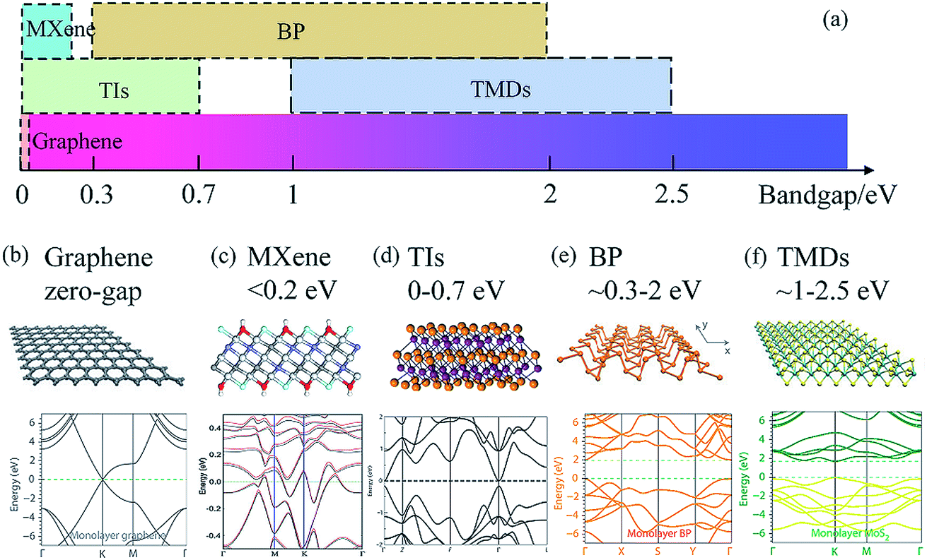 | ||
| Fig. 1 (a) Distribution diagram of the bandgap of 2D materials. The atomic structures and band structures (monolayer) of graphene, (b) MXene, (c) TIs, (d) BP (e) and TMDs (f). This figure has been adapted from ref. 37, 61, 69 and 76 with permission from Nature Physics, Advanced Materials, Nature Photonics, Journal of the American Chemical Society. | ||
MXenes, graphene-like layered materials, are an emerging LDM with the characteristics of metal, carbon, nitrogen and a carbon–nitrogen main layer. Mn+1XnTx is the chemical formula of MXenes, where M represents a transition metal, X represents carbon, or carbon–nitrogen, Tx represents a terminated functional group (–OH, –O or –F), and n can have a value of 1, 2, or 3.52 The atomic structure of MXene has been illustrated in Fig. 1(c),61 and the bandgap of MXenes is less than 0.2 eV which is close to that of graphene (Fig. 1(a)).61 The linear absorption and nonlinear absorption efficiency of MXenes is about 1%/nm and –10−21 m2 V−2,43 respectively. The MXene Ti3C2Tx with a thermal conductivity of 56 W m−1 K−1 possesses strong energy conversion efficiency (∼100%).74 Compared with other LDMs, MXenes are more flexibility due to the high threshold for photo-induced damage, and have considerable application prospects in the field of all-optical devices.15,16,42,43,56,75 In addition, the comprehension of optical material interactions and nonlinear optical properties is still in the preliminary stage.
Topological insulators (TIs) of group V chalcogenides also have a layered structure with a large interlayer van der Waals gap.76 And TIs are novel electronic and quantum materials with internal insulation and electrical conduction at the surface or edge. Owing to the strong spin orbit coupling, TIs have a Dirac cone structure, which is similar to that of graphene. The energy band structure of TIs matches that of the traditional insulator, and the Fermi energy level is between the conduction band and valence band. The surface state of TIs depends on the topological structure, which is hardly affected by impurities and disorder. The bandgap of TIs is about 0–0.7 eV (Fig. 1(d)),37 which can be engineered by changing the thickness or fabricating heterostructures with different TIs.37,76–79 The small bandgap of TIs makes them promising for photo-absorption over a broad spectral range. To date, some TI materials have been confirmed in experiments, such as Sb2Se3, Bi2Se3, Bi2Te3 and Sb2Te3. These materials have widely been applied in the field of electronics and optoelectronics.
BP, where each phosphorus atom is bonded by three adjacent phosphorus atoms to form a honeycomb structure, whose monolayer is called phosphorene, is a direct bandgap semiconductor from monolayer (2 eV) to few layers (0.3 eV),80 as displayed in Fig. 1(e).69 Its bandgap can be modified by altering the number of layers. It might compete with graphene due to the high electron mobility, strong light matter interaction and thickness dependent direct energy bandgap in the infrared or even mid-infrared regime.81 However, its sensitivity to oxygen and water has set a barrier for long-term device applications. Recently, many fabrication methods of phosphorene have been investigated to improve the stability of BP. And fluorinated phosphorene has been used to implement all-optical switches and logic gates.14,66 Subsequently, a series of black phosphorus analogues (BPAs), such as tellurene, bismuthene,12,82 and antimonene,11,22,66,83 have been extensively studied for several years. They have a similar folded structure as BP and exhibit a high photothermal effect, tunable bandgap, and strong optical absorption but with high stability under ambient conditions. Recently, the thermo-optic effect of LDM bismuthene and antimonene has been applied for all-optical switching.
TMDs are a cluster of compounds with a general chemical formula MX2, where M stands for the transition metal elements and X is a chalcogen. Due to their excellent performance in electronics and optoelectronics, they have attracted great attention from researchers in the fields of physics, chemistry and materials. In the bulk state, they are semiconductors with an indirect bandgap. However, when exfoliated to monolayers, they exhibit a direct bandgap. The bandgap of TMDs ranges from ∼1 to 2.5 eV (Fig. 1(f)).69 Several studies have found that TMDs have a broadband tunable band gap, high carrier mobility, and exhibit excellent third-order nonlinear optical properties, including broadband saturation absorption, two-photon absorption, and high nonlinearity. The thermo-optic effect of MoS2 and WS2 has been explored for all-optical phase shifters and switches.13,19
CNTs, especially single-wall carbon nanotubes, have gained widespread attention because of their excellent electrical and optical properties. They have distinctive advantages, such as ultra-fast recovery time and wide absorption bandwidth. The recovery time of single-wall carbon nanotubes has been measured to be <1 ps by using a pump-probe method.21,23 Their saturable absorption and thermo-optic properties have been utilized for generating ultrafast optical pulses84 and implementing the quasi-autocorrelation technology.62
High quality LDMs are crucial in an all-optical device, and provide important flexibility in practical application. Three fabrication methods of LDMs are mainly used in all-optical applications. They are chemical vapor deposition (CVD), mechanical exfoliation and liquid-phase exfoliation (LPE).
Chemical vapor deposition is a significant method to produce abundant LDMs. Generally, gaseous and powdery reactants are placed into a tube furnace, and LDMs can be produced by the specific chemical reaction at a appropriate temperature. By placing the substrate downstream, LDMs grow on the surface of the substrate.85 In addition, the number of layers of LDMs can be controlled precisely with a good accuracy by modifying the reaction parameters. High yield makes this method the main method for commercial large-scale production of LDMs.86
Mechanical exfoliation was first used for discovering two-dimensional graphene from graphite flakes by K. S. Novoselov and A. K. Geim in 2004.87 This method is also applied for preparing other LDMs.88–90 Many few- or mono-layer LDMs take advantage of van der Waals forces to gather together and constitute the bulk materials. Therefore, researchers can obtain high-quality LDMs by overcoming the van der Waals force to break apart the bulk materials. This method uses Scotch tape to peel the surface of the bulk material repeatedly for obtaining few- or mono-layer LDMs.91 It is easy to carry out compared with chemical vapor deposition. However, repeated operation is essential in the whole process, which leads to a low yield accordingly.
Liquid-phase exfoliation starts from large flakes of raw materials. In this method the powdery material was put into a specific solvent, such as the organic solvent NMP; this method uses high-intensity long-time sonication to shatter the material powder into mono or few-layer material nanosheets, and separates the material nanosheets from the unbroken bulk material by centrifugation.92,93 After standing for a while, the large-sized material particles will sink to the bottom of the solvent, and the small-sized material nanosheets will be suspended in the upper layer. The upper layer of the solvent is collected using a pipette to obtain a mixture of the material nanosheets and the solvent. It is hard to precisely control the size and number of layers of LDMs obtained by this method. However, it is a simple, high-yield and low-cost method to produce LDMs.94
Fiber all-optical devices with the thermo-optic effect
As we have mentioned, the main mechanisms for LDM based fiber all-optical control are the thermo-optic effect and saturable absorption. Here, we first review the applications based on the thermo-optic effect of LDMs, i.e., all-optical modulators, switches and logic gates. The system structures of these fiber all-optical devices can be generally classified into 2 main categories: non-resonant and resonant designs. For non-resonant designs, three typical designs will be discussed: they are Mach–Zehnder interferometer (MZI),14,16,18–20 Michelson interferometer (MI),11,12,67 and polarization interferometer (PI).13 For resonant design, micro-rings95 will be discussed.Moreover, compared with other effects such as Kerr nonlinearity, although thermo-optic devices have a relatively slow response, they require less pump peak power to drive the devices. This leads to less energy consumption when the device is required to hold a state for a long time, e.g., milliseconds. Therefore, thermo-optic all-optical devices are an indispensable member in the family of all-optical devices.
Fiber all-optical devices with an MZI structure
Fig. 2(a) shows the typical structure of an MZI-based all-optical device.16 The device structure consists of an all-fiber MZI. The LDM MXene is deposited on a microfiber and incorporated into the upper arm of the MZI. Two 980/1550 wavelength division multiplexers (WDM1 and WDM2) are placed before and after the microfiber. 980 nm control light (pump) is injected through WDM1 and extracted through WDM2. A delay line and a variable optical attenuator (VOA) are placed in the lower arm of the MZI to balance the optical length difference and optical power in the two arms. MXenes exhibit strong absorption at 980 nm, so the injected 980 nm control light (pump) will be absorbed by the MXene and heat it. Due to the thermo-optic effect of both the MXene itself and microfiber, the 1550 nm signal light propagating through the MXene deposited microfiber will change its phase. So it forms an all-optical phase shifter. The phase change will be converted to output power change by the MZI.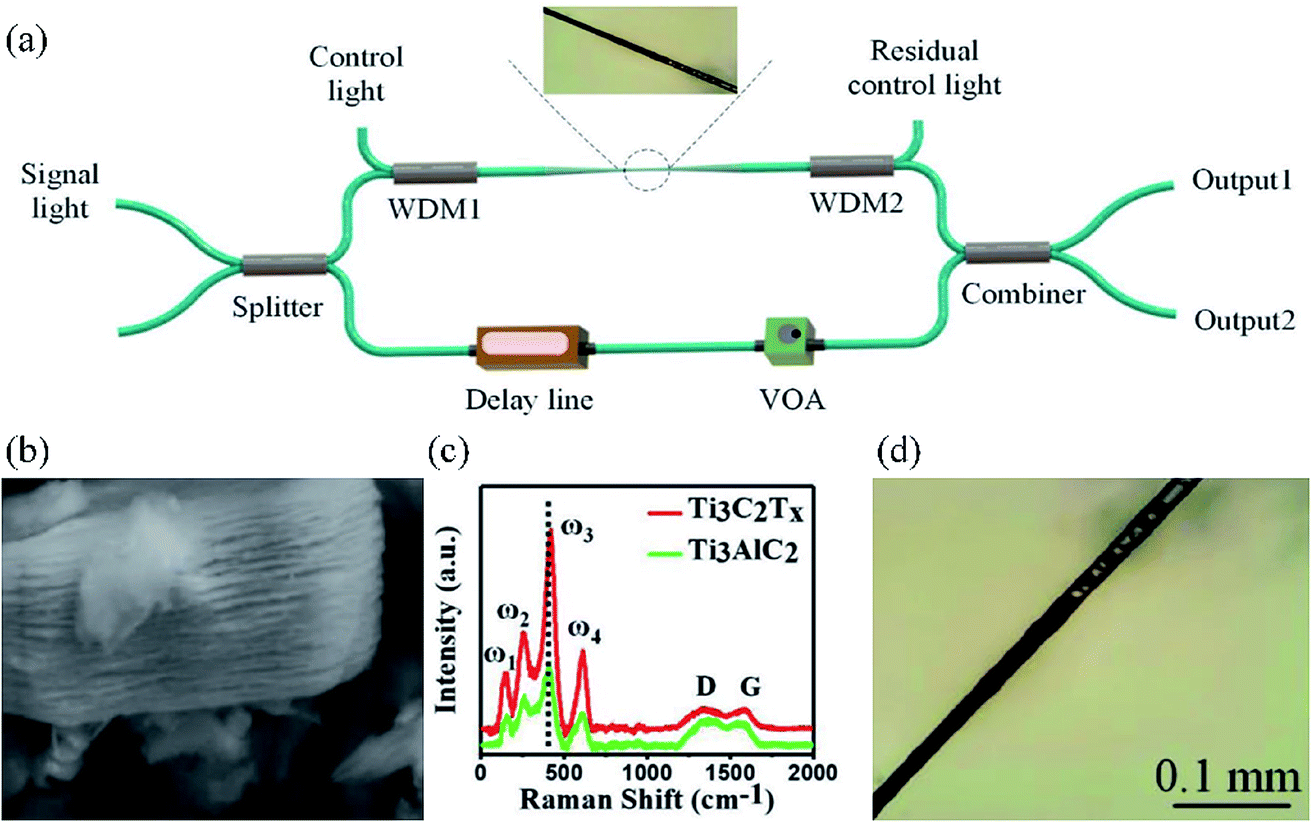 | ||
| Fig. 2 (a) Experimental setup of an MZI all-optical modulator based on MXene materials. (b) High-resolution electron microscopy image of MXene nanosheets. (c) Raman spectrum of Ti3AlC2 and Ti3C2Tx. (d) Optical microscopy image of microfibers deposited with MXenes. This figure has been adapted from ref. 16 with permission from Advanced Materials. | ||
The MXene deposited microfiber is the key component in the all-optical control system. The MXene Ti3C2Tx was synthesized by the liquid-phase exfoliation method (aqueous acid etching method). Briefly, a Ti3AlC2 di-ionic solution was mixed with hydrofluoric at a certain ratio and the delaminating process happened at an appropriate temperature. After that, the precipitate was washed with deionized water and the MXene powder was dispersed in an isopropyl alcohol solution. Then, few-layer MXene nanosheets can be obtained by centrifuging the isopropyl alcohol solution. Fig. 2(b) shows the high-resolution electron microscopy image of MXene Ti3C2Tx nanosheets. The Raman spectra of Ti3AlC2 and Ti3C2Tx were measured, as shown in Fig. 2(c). An optical deposition method was used to fabricate the MXene-based device by dropping the MXene dispersion onto the side face of the microfiber. Fig. 2(d) shows the optical microscope image of the microfiber with a 500 μm deposited length.
In the experiment, an amplified spontaneous emission (ASE) source near 1550 nm is first used to characterize the modulation properties. For a balanced MZI as shown in Fig. 2(a), its two outputs (denoted as “Output 1” and “Output 2” in Fig. 2(a)) can be expressed by Pin(1 − cos(kΔL))/2 and Pin(1 + cos(kΔL))/2 respectively, where Pin is the input power, k is the propagation constant and ΔL is the length difference of the two arms in the MZI. From these two equations, we can observe that the output powers of these two outputs are complementary, i.e., their total power is fixed to Pin (assuming a lossless system for simplicity) and one reaches the maximum when the other reaches its minimum. As shown in Fig. 3(a), the output spectra at both “Output 1” and “Output 2” ports have comb-like structures and are complementary to each other. Fine tuning the loss in two arms enables a good extinction ratio. When the 980 nm control light (pump) is applied, the MXene deposited microfiber absorbs the control light (pump) power, generates heat and shifts the optical phase of the signal light. This phase shift equivalently changes the length difference between two arms and thus leads to an FSR (free spectral range) change and a spectral shift. Shifting by 1 FSR represents a phase shift of 2π. Therefore, the phase shift can be measured by observing the spectral shift. In Fig. 3(b), the red dashed curve represents a spectral shift of 4.5 FSRs, corresponding to a phase shift of 9π. The relationship between the control light (pump) power and the phase shift is shown in Fig. 3(c) and a control efficiency of 0.074π/mW is obtained.
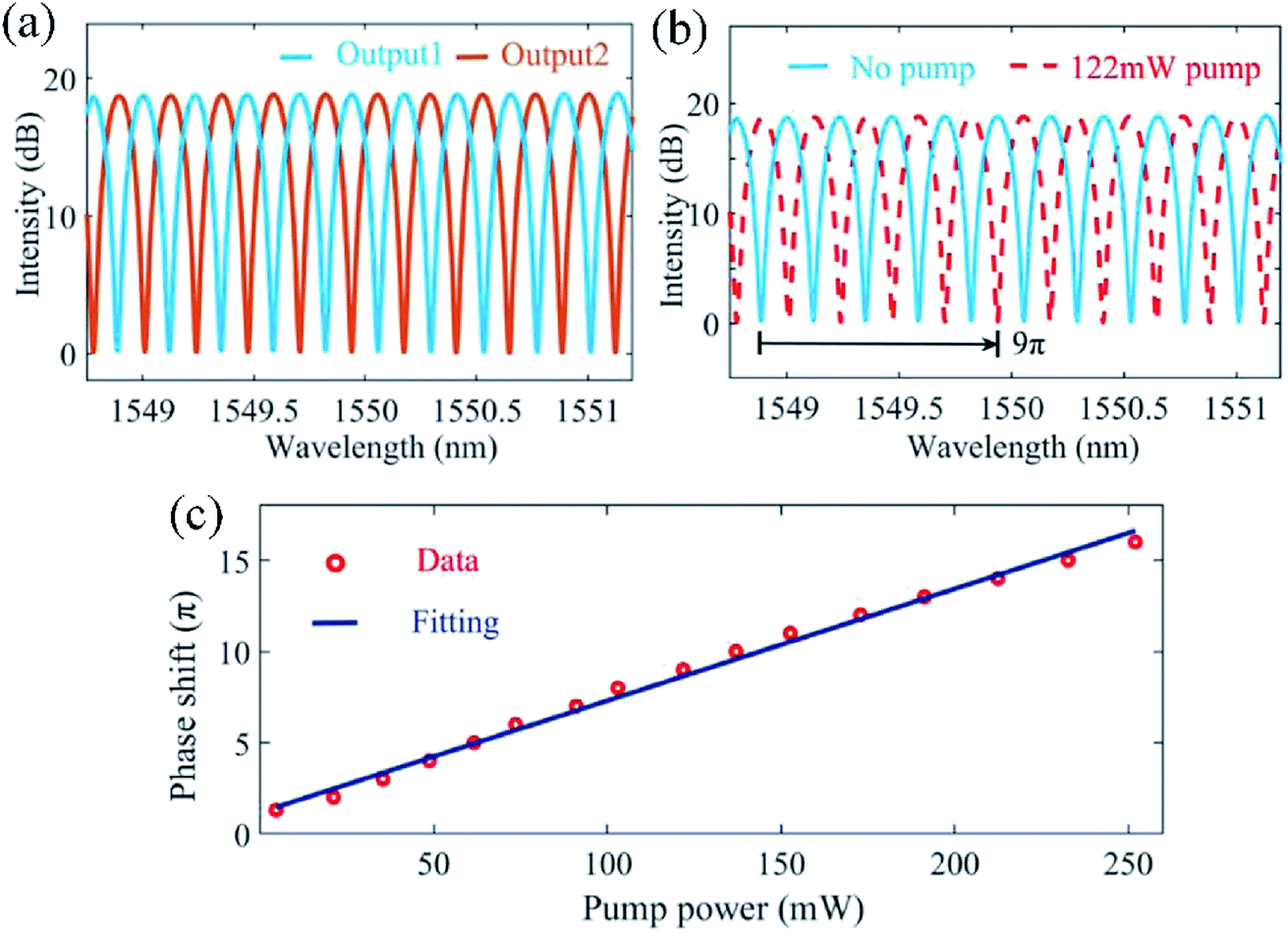 | ||
| Fig. 3 (a) Interference spectra of two output ports. (b) Interference fringes at a control light (pump) power of 122 mW. (c) Phase shift versus different control light (pump) powers. This figure has been adapted from ref. 16 with permission from Advanced Materials. | ||
An all-optical switch for the MXene-based device is then demonstrated. Here, a 1550 nm continuous wave (CW) laser source is used as the signal light. The control light (pump) is the pulsed 980 nm light shown in Fig. 4(a). Fig. 4(b) shows the waveform of the switch output at “Output 1” and “Output 2” ports, when the control light (pump) with 120 mW is applied to the all-optical control system. The 1550 nm signal light is controlled by the 980 nm light and the waveforms of “Output 1” and “Output 2” are complementary to each other. By fitting the measured output waveform of signal light with the exponential function, the time constant of the rising (falling) edge is estimated to be 4.10 ms (3.55 ms). The time constant of the rising edge depends on the fact that the MXene absorbs control light (pump) to increase the temperature and air convection causes heat dissipation. The time constant of the falling edge only depends on the heat dissipation of the MXene deposited microfiber. The relationship between the output optical power and the phase shift can be simplified as follows:
| Pout ∝ 1 − cos(ΔΦ) |
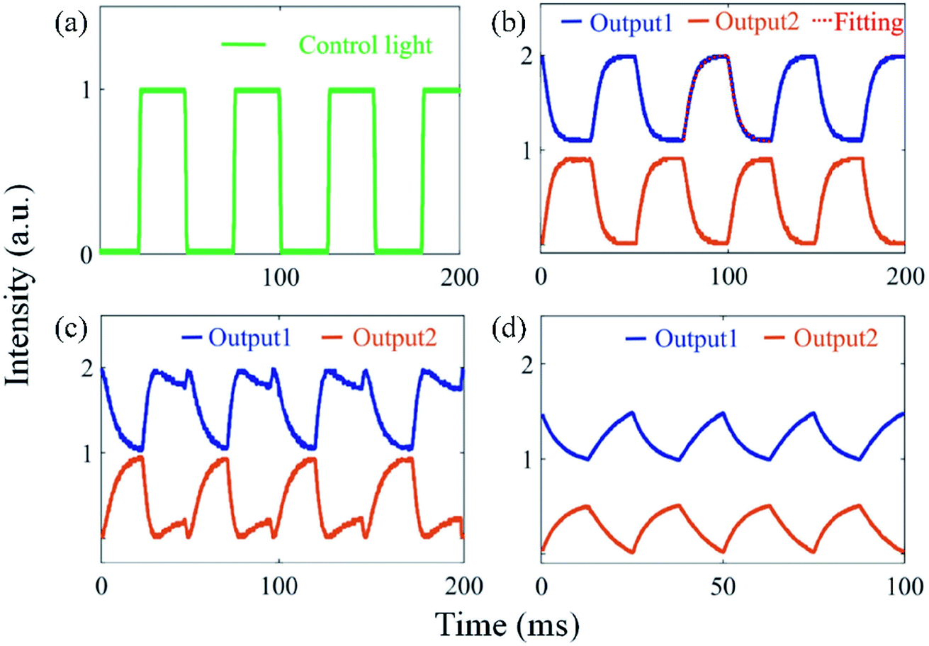 | ||
| Fig. 4 (a) Waveform of the control light (pump). (b) A single on–off transition of the signal light and the corresponding fitting curve. (c) Output breaking. (d) Waveforms of signal light at 40 Hz. This figure has been adapted from ref. 16 with permission from Advanced Materials. | ||
Fiber all-optical devices with a MI structure
The device performance can be further improved by the new design with a Michelson interferometer structure, as shown in Fig. 5(a).12 The MZI structure in Fig. 2(a) is sensitive to environmental perturbation due to the instability of fiber-type MZIs. Fig. 5(a) shows a new all-optical switch using a fiber-type MI with a bismuthene deposited microfiber in one arm. Here, the LDM bismuthene quantum dots are synthesized by a liquid-phase exfoliation method and then deposited onto a microfiber. Two Faraday rotation mirrors (FRM 1 and FRM 2) are applied to eliminate the polarization interference problem caused by the perfect orthogonality between the input and output polarization states. The VOA is used to adjust the power in two arms to obtain a more stable output signal.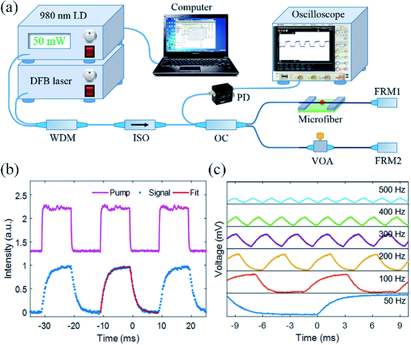 | ||
| Fig. 5 (a) A MI fiber all-optical modulator based on bismuthene material. (b) Waveforms of control light (pump) and signal light and the corresponding fitting curve. (c) Signal waveforms at different modulation frequencies of control light (pump). This figure has been adapted from ref. 12 with permission from Journal of Materials Chemistry C. | ||
Fig. 5(b) shows the output signal light with the same frequency and duty cycle as the 980 nm control light (pump), indicating that the signal light has been modulated.12 By exponential fitting, the output signal pulse has a much faster rising time constant of 1.56 ms and a falling time constant of 1.53 ms, compared with the all-optical modulator using the MXene deposited microfiber. The response time is related to the heat generation from the control light (pump) and the heat dissipation to the air. Compared with the MZI system, light propagates through the LDM twice due to the reflection structure of the MI, which leads to both improved pumping efficiency and phase shift of signal light. As a result, the response time in the MI is typically faster than that in the MZI. To further investigate the frequency characteristics of the all-optical system, the 980 nm control light (pump) is modulated from 50 Hz to 500 Hz externally at a fixed power of 60 mW. It can be clearly found that the shape of the output signal light is gradually deformed from a square waveform to triangle waveform, as shown in Fig. 5(c). The peak to peak voltage reduces as the modulation frequency increases. These phenomena can be attributed to the slow response of heat generation and dissipation processes in the bismuthene deposited microfiber.
Besides the applications of all-optical modulators and switches, the MZI and MI structures based on the thermo-optic effect of LDMs can be also applied for all-optical logic gates.12 The output depends on both the control light (pump) and input signal light and thus the output waveform can be treated as a logic operation between the control light (pump) waveform and the input signal light waveform. In the experiment, the control light (pump) carrying a binary sequence “1101011010010101” is applied to the all-optical system as the input information source. The input signal light is set to all “1”. The control light (pump) and the measured output signal light at two different logic states are shown in Fig. 6. It can be observed that the two output states of the signal light copy either the binary sequence of the control light (pump) or its “NOT” state. When the control light (pump) carries information, this process transfers the information to the signal light. Therefore, it is promising that the all-optical system based on the thermo-optic effect has great potential applications in all-optical information processing and all-optical communication.
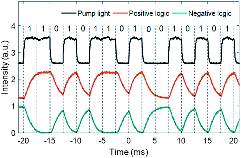 | ||
| Fig. 6 ACSII codes carried by control light (pump) and modulated signal light. This figure has been adapted from ref. 12 with permission from Journal of Materials Chemistry C. | ||
Fiber all-optical devices with a PI structure
To further improve the switching rate of the all-optical system based on LDMs, a fiber polarization interferometer structure is demonstrated with molybdenum disulfide (MoS2)-polyvinyl alcohol (PVA) thin films, as shown in Fig. 7(a).13 The MoS2-PVA thin film is fabricated by the liquid-phase exfoliation method. 980 nm control light (pump) and 1550 nm signal light are combined by the WDM. Polarization controllers (PCs) are used to control the polarization states of the two light beams. The MoS2-PVA thin film is sandwiched between two angled physical contact (FC/APC) fiber connectors. A second WDM after the MoS2-PVA thin film filters out the residual 980 nm control light (pump). A polarizer is used to select the desired polarization of the signal light and generate the modulated 1550 nm signal light.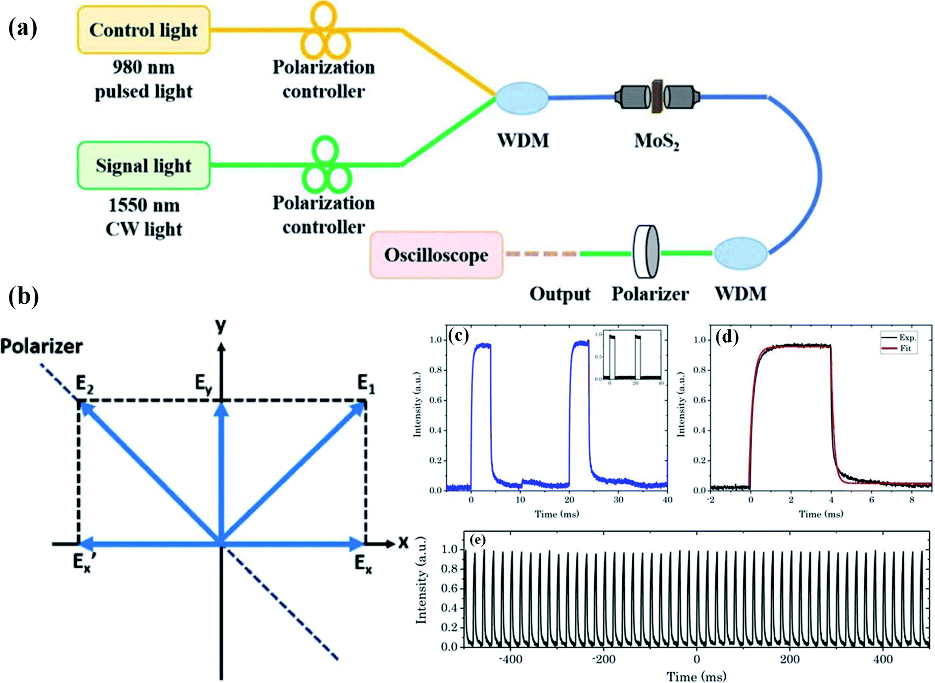 | ||
| Fig. 7 (a) A PI fiber all-optical modulator based MoS2-PVA thin films. (b) Device principle. (c) Waveform of signal light, inset: waveform of control light (pump). (d) A zoomed view of a single off–on–off transition of the signal light and the corresponding fitting curve. (e) Output signal light in a long-time region. This figure has been adapted from ref. 13 and 96 with permission from Chinese Optics Letters, Photonics Research. | ||
The principle can be explained from Fig. 7(b).96 The x–y plane is perpendicular to the direction of light propagation. By adjusting the polarization controllers, the polarization of the signal light is set to E1 with equal projection Ex and Ey on the x and y axes and is perpendicular to the direction of the polarizer (along E2 in Fig. 7(b)). As a result, the output signal power after the polarizer is low. When the 980 nm control light (pump) is injected into the all-optical system, the MoS2-PVA thin film absorbs the control light (pump) and generates heat. However, the non-uniform distribution of MoS2 nanosheets in the PVA thin film leads to a non-uniform heat distribution, which leads to a non-uniform index change and unequal phase shift to Ex and Ey. Thus, the relative phase of Ex is shifted by π and Ex becomes  . The new polarization direction of the signal light becomes E2, which leads to a high output signal power.
Fig. 7(c) shows the modulated output signal light and the waveform of the input control light (pump) (inset). By fitting the exponential decay functions as shown in Fig. 7(d), the time constants for the rising edge and the falling edge can be estimated to be 324.5 μs and 353.1 μs. Compared with the LDMs deposited on microfibers, the thin film allows much faster heat distribution and thus results in a much faster switching time. Moreover, two interference light beams (two polarization states) propagate in the same fiber in the PI structure and thus the PI structure is less sensitive to environmental perturbation than the MZI and MI structures. A long-term output pulse train is shown in Fig. 7(e) and a very stable pulse amplitude can be observed.
Here, we briefly summarize current progress in thermo-optic fiber all-optical devices based on LDMs. A comparison among recent studies is provided in Table 1. For the fiber MZI devices, four studies have been performed with graphene, WS2, MXenes, phosphorene and boron. The work with boron obtained a relatively fast rising time constant of 0.48 ms due to the superior photo-thermal response.20 The work with graphene shows 0.51π phase shift at a low pump power of 5.3 mW due to the long interaction length of LDM graphene.18 For MI structures with LDMs, three studies have been performed with antimonene, bismuthene and MXene respectively. A very good extinction of 27 dB is obtained in the work with MXenes. The work with bismuthene also showed a fast rising time constant of 1.56 ms. The PI structure with the MoS2-PVA thin film is less sensitive to environmental perturbation and has a very fast rising time constant of 324.5 μs due to the short interaction length. The micro-ring structure with graphene has a faster modulation speed of ∼134 μs due to the thin diameter of the microfiber.95
| Device | Form | Rising time constant | Falling time constant | Extinction ratio (dB) | Slop (π/mW) | Ref. |
|---|---|---|---|---|---|---|
| Fiber MZI w/graphene | Microfiber | 4 ms | 1.4 ms | 20 | 0.091 | 18 |
| Fiber MZI w/WS2 | Microfiber | 7.3 ms | 3.5 ms | 15 | 0.0174 | 19 |
| Fiber MZI w/MXene | Microfiber | 4.10 ms | 3.55 ms | 18.53 | 0.061 | 16 |
| Fiber MZI w/phosphorene | Microfiber | 2.5 ms | 2.1 ms | 17 | 0.029 | 14 |
| Fiber MZI w/boron | Microfiber | 0.48 ms | 0.69 ms | ∼10.5 | 0.01329 | 20 |
| Fiber MI w/antimonene | Microfiber | 3.2 ms | 2.9 ms | 25 | 0.049 | 11 |
| Fiber MI w/bismuthene | Microfiber | 1.56 ms | 1.53 ms | 25 | 0.076 | 12 |
| Fiber MI w/MXene | Microfiber | 2.3 ms | 2.1 ms | 27 | 0.034 | 67 |
| Fiber PI w/MoS2 | Thin film | 324.5 μs | 353.1 μs | 10 | NA | 13 |
| Fiber micro-ring w/graphene | Microfiber | ∼134 μs | ∼96 μs | 13 | 0.0558 | 95 |
All-optical control with saturable absorption
Besides the thermo-optic effect, another main mechanism for LDM based fiber all-optical control is saturable absorption. LDMs with saturable absorption have been widely utilized in mode-locked and Q-switched lasers.43,80,82,85,97–105 In this section, we review all-optical light manipulation with saturable absorption of LDMs. Here, two demonstrations are provided. They are an all-optical thresholder for noise suppression65,66,68 and quasi-autocorrelation for pulse characterization,62 also called saturable absorption based pulsewidth measurement (SAPM).All-optical thresholder with saturable absorption
Recently, all-optical signal processing is gradually becoming an important aspect in optical communication systems because of the increasing demand for high speed and high capacity communication systems. All-optical signal processing based on LDMs provides an effective method to achieve high speed and high capacity communication systems by utilizing the strong light interaction in LDMs. It has been recognized that because of the nonlinear property of LDMs, saturable absorption is required for a highly stable and effective all-optical thresholder.65,66,68 Several technologies for the all-optical thresholder have been reported, such as the second harmonic generation (SHG) effect in period lithium niobate,106 cross gain modulation effect in distributed-feedback semiconductor lasers, black phosphorus based optical thresholders.68 However, the performance of these technologies is limited by their poor stability. And antimonene, as an ultra-stable material, is proposed to be an ideal nonlinear material for the all-optical thresholder.66Few-layer antimonene (FLA) is prepared by the liquid-phase exfoliation method. And then, it is deposited onto a piece of microfiber, which is fabricated by using the flame taper method. To further understand the light–matter interaction effect in the few layer antimonene decorated microfiber, the nonlinear property of saturable absorption is investigated by measuring the input-power-dependent transmission through a femtosecond pulse laser. The laser source is amplified using an erbium-doped fiber amplifier and a tunable optical attenuator is used in the optical path to adjust the incident power onto the microfiber continually. The incident laser source is divided into two optical paths by the coupler: one injected into the FLA decorated microfiber and connected the optical power meter and the other directly connected to another optical meter with the same parameter as a reference. By tuning the loss of the optical attenuator, the transmission of the few layer deposited microfiber with an optical modulation depth of 6.4% is obtained, as shown in Fig. 8.
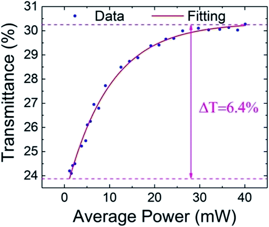 | ||
| Fig. 8 Saturable absorption curve of antimonene material. This figure has been adapted from ref. 66 with permission from 2D Materials. | ||
It has been experimentally demonstrated that FLA is an effective saturable absorber. Therefore, it is expected that the FLA decorated microfiber can be utilized for all-optical thresholders for ultrashort pulse shaping. Optical pulses will experience higher transmission than the noise when passing through the optical thresholder. As the noise experiences stronger attenuation than pulses, the signal to noise ratio (SNR) of pulses will be improved after passing through the FLA based optical thresholder.
Fig. 9(a) shows the experimental design of an all optical thresholder.66 A passively mode locked fiber laser is used as the pulse source and a 1 GHz radio frequency modulated lower power light is utilized as the noise source. Their waveforms are shown in Fig. 9(b) and (c) respectively. The pulse source and noise source are combined together as a noise source using a 50:50 coupler, as shown in Fig. 9(d). For comparison, the combined optical pulse is divided into two paths: one path passing through the FLA based microfiber experiences the saturable absorption effect and the other one is directly connected to the optical power meter to monitor the input optical power of the FLA sample. Based on the saturable absorption effect, the noise in the pulses will be absorbed by the FLA sample when pulses pass through. As a result, the optical pulses passing through the FLA sample are expected to have an enhanced SNR. To measure the absorption strength at different input optical powers, an erbium doped fiber amplifier combined with a tunable optical attenuator is adopted to adjust the optical power before the FLA based microfiber.
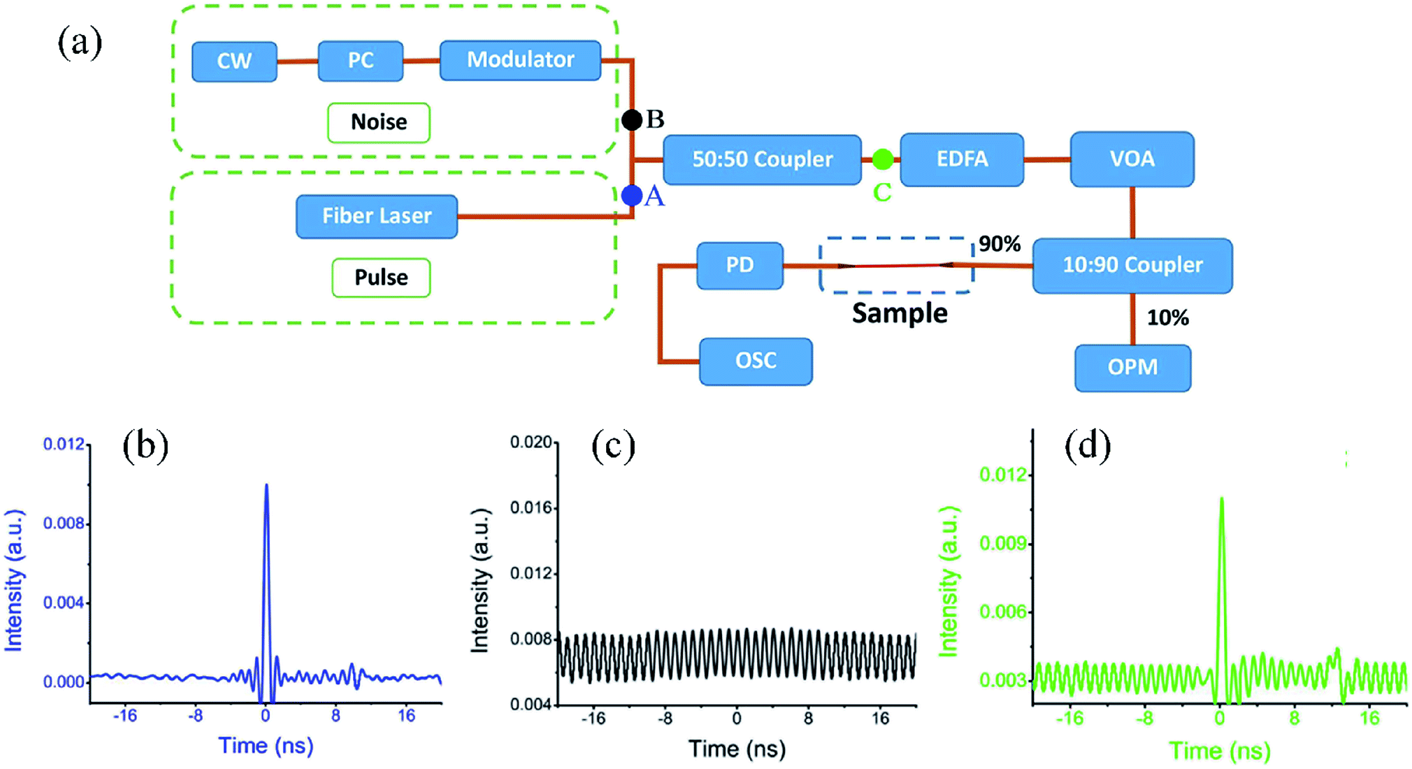 | ||
| Fig. 9 (a) Experimental diagram of all-optical thresholder. (b) Pulse profile of the fiber laser source. (c) Pulse trace of the noise. (d) Combined pulse trace including the fiber laser source and noise source. This figure has been adapted from ref. 66 with permission from 2D Materials. | ||
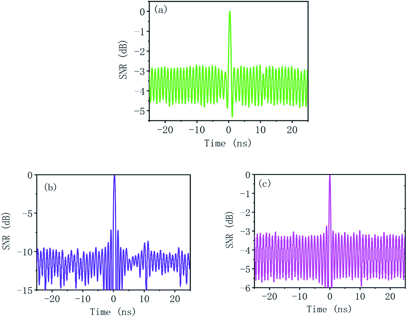
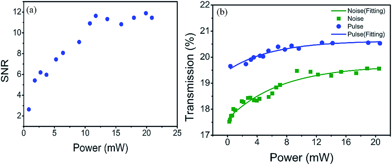
Fig. 10(a) and (b) show the optical pulses before and after passing through the FLA based microfiber.66 It is easy to observe from the figures that the SNR is improved significantly after passing through the sample. To confirm that the optical thresholder is attributed to the function of FLA rather than the microfiber, a bare microfiber without the FLA sample is inserted into the cavity for the SNR measurement. Fig. 10(c) shows that the optical pulses are still noisy and the SNR has not improved substantially.66 Therefore, it can be deducted that it is the saturable absorption of antimonene which acts as an optical thresholder in the experiment. To further illustrate the performance of the FLA sample as an all optical thresholder, we measure the SNR of output pulses passing through the sample under different input optical powers. The experimental result is shown in Fig. 11(a).66 It shows that as the input optical power gradually increases to higher than 10 mW, SNR enhancement remains at 12 dB. This indicates that the sample is saturated at 10 mW and the maximum SNR enhancement of noisy pulses is 12 dB. To confirm the experimental results, the transmission rate of pulses and noises under different powers is measured and shown in Fig. 11(b).66 It is obvious that the transmission of the pulse is always higher than that of the noise and the sample is saturated by the pulse at a low power. However, the transmission of noise gradually increases as the power increases and tends to be saturated when the power of noise increases to 10 mW. Finally, the long term stability of this all optical thresholder is demonstrated by measuring the output waveform each hour for 8 h. These results indicate that the FLA decorated microfiber can be developed an effective, stable all optical thresholder.
 | ||
| Fig. 10 (a) Pulse envelope before passing the FLA sample based optical thresholder (b) pulse envelope after passing the FLA sample. (c) Pulse envelope after passing the bare microfiber without the FLA sample inserted. This figure has been adapted from ref. 66 with permission from 2D Materials. | ||
 | ||
| Fig. 11 (a) SNR ratio versus different pump powers. (b) Transmission rate of noise and pulses after passing through the FLA-decorated microfiber and the corresponding fitting curve. This figure has been adapted from ref. 66 with permission from 2D Materials. | ||
Quasi-correlation with saturable absorption
Autocorrelations (ACs) based on second harmonic generation (SHG) and two-photon absorption (TPA) have been two main key technologies to characterize ultrashort pulses over the past few decades.107–109 However, there are still some shortcomings for these methods. For example, light at different wavelengths may require phase matching for optimizing the second harmonic generation. The TPA effect often has picosecond decay time in bulk semiconductors, which may lead to some limitations for pulse width measurement.110–112On the other hand, the saturable absorption of the LDM carbon nanotubes makes them the nonlinear medium for pulse interactions, which is the key requirement for the pulse width measurement. Most LDMs have exhibited femtosecond level decay time, which makes them promising to minimize the distortion for measuring the ultrashort pulses, compared with two-photonic absorption. In addition, the atomic level thickness of the LDMs can minimize the pulse broadening caused by fiber dispersion. The integration technology between LDMs and the optical system or LDMs and the planner waveguide has been highly developed. Therefore, quasi-autocorrelation may provide a novel method to measure an ultrashort pulse.
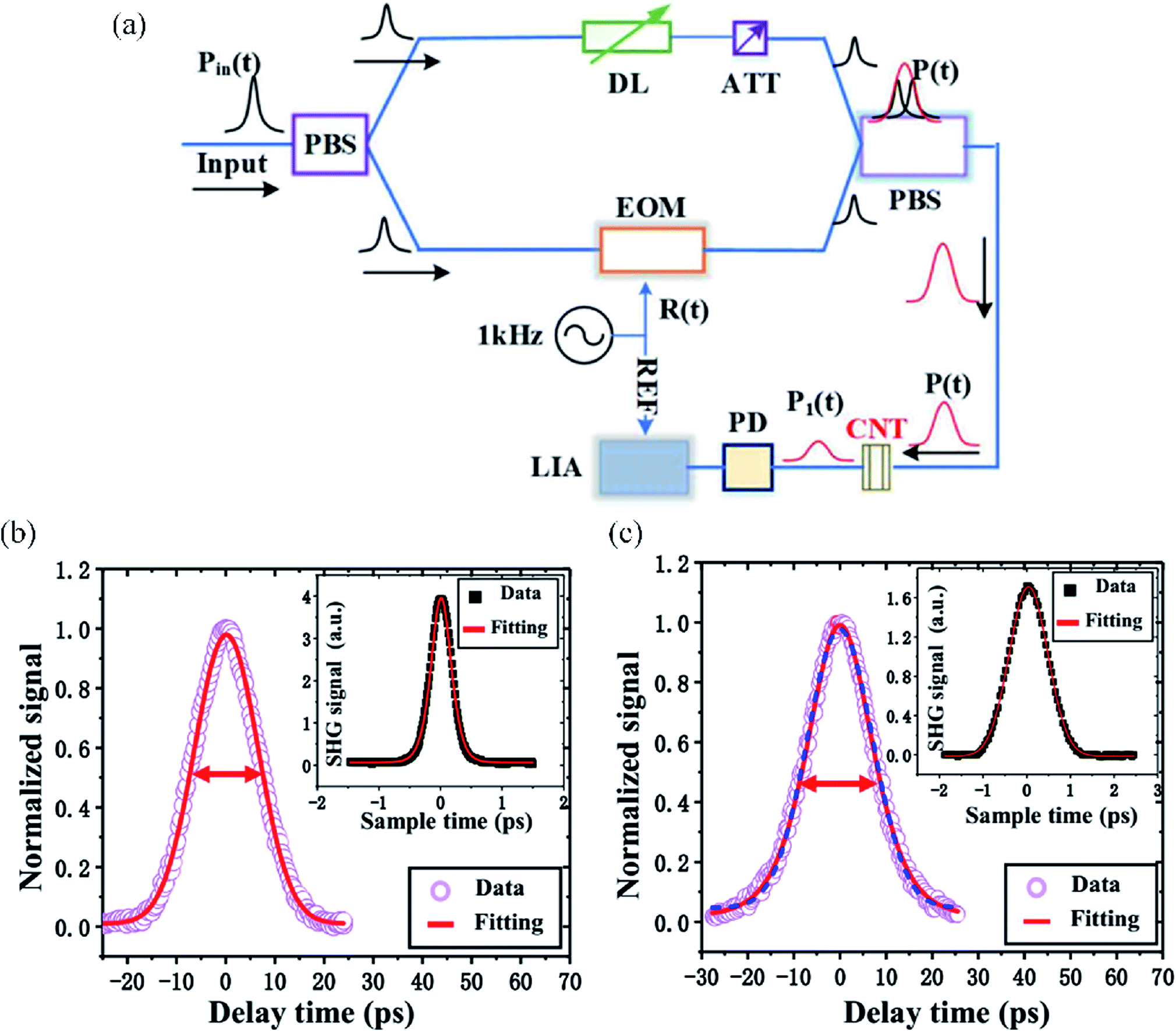
Fig. 12(a) shows the pulse width measurement system based on LDM carbon nanotubes, which is very similar to traditional intensity autocorrelation.62 The input optical pulse is divided by the polarizer beam splitter. One of the split pulses is modulated by the electro-optic modulator and the other optical pulse passes through the time delay line and a tunable attenuator which is used to balance the power of two different branches. Polarization maintaining optical fiber devices are used to avoid the interference between the two paths. Then, the two optical pulses are combined by another polarizer beam splitter and propagate through the LDM carbon nanotube. The output signal of the material is detected by the photodetector and measured with a lock-in amplifier (LIA) system.
 | ||
| Fig. 12 (a) Schematic diagram of the SAPM system based on CNTs. (b) SAPM trace (purple circles) and Gaussian fit (red line), inset: AC trace with a standard SHG autocorrelator. (c) SAPM trace (purple circles), hyperbolic secant fit (red line) and Gaussian fit (blue dashed line), inset: AC trace with a standard SHG autocorrelator. This figure has been adapted from ref. 62 with permission from Optics Express. | ||
A typical SAPM experimental result is shown as purple circles in Fig. 12(b).62 The data point is averaged by 100 times to reduce the noise from environment perturbation. The horizontal axis is the time delay of two pulses and the vertical axis is the measured LIA signal amplitude. The input signal pulse has a bandwidth of ∼57.2 nm, a repetition rate of 100 MHz and a center wavelength of 1560 nm. The pulse peak power at the input port of the system is 23.635 W and the pulse peak power entering the CNT saturable absorber is 0.345 W (zero delay between two arms), which is mainly caused by pulse broadening induced by fiber dispersion and system loss of 7.71 dB. The red curve is the fitted SAPM pulse profile using a Gaussian shape, which has a pulse width of ∼11.94 ps broadened by the dispersion of the system. Therefore, the calibration in the system is crucial. An AC trace is also measured by standard SHG autocorrelation with a pulse width of 1.03 ps, as shown in the inset of Fig. 12(b). Fig. 12(c) shows the SAPM trace of a soliton pulse with a hyperbolic secant profile and the inset of Fig. 12(c) shows the corresponding standard SHG AC trace.
After obtaining the pulse profile based on the saturable absorption pulsewidth measurement method, there are still two calibration steps to be completed.62 The all-optical control system avoids alignment, but makes the pulse dispersion broadened. The conversion coefficient Ccon is the ratio of the input pulse width to the pulse width of the measured autocorrelation trace, which is dependent on the nonlinear transmission of the LDM carbon nanotubes. First, the conversion coefficient is determined by comparing the input pulse width and the measured pulse width of the system. Then, the dispersion broadening effect caused by the fiber system dispersion is determined.
The stability and sensitivity of the system are also investigated by measuring pulses 30 times over a long period of time and reducing the input average power to discover the minimum detectable power.113Fig. 13(a) shows the long-term SAPM traces, indicating that the measurement results are stable under environment disturbance. Fig. 13(b) exhibits the typical the SAPM trace with a minimum detectable input power of −21.26 dBm. Compared with the input pulse width of 895 fs, the pulse width of the measured SAPM pulse is 11.78 ps. It has an acceptable deviation (13.5%) in low input power. These results indicate that the quasi-autocorrelation SAPM technology shows promise as an efficient, stable and compatible pulse width measurement.
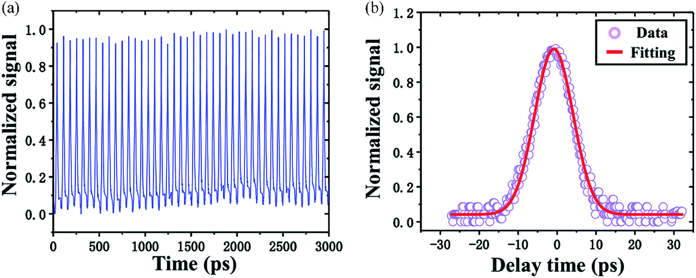 | ||
| Fig. 13 (a) Pulse train of the SAPM for a long time. (b) SAPM measurement result with a pulse energy of 75 fJ. This figure has been adapted from ref. 62 with permission from Optics Express. | ||
We also compare the properties of two current AC technologies SHG and TPA with the quasi-AC SAPM technology, shown in Table 2. First, SHG technology is very flexible in beam alignment because it does not need phase matching. Second, LDMs used in the SAPM system and TPA materials are easy to integrate into various integration platforms.114 However, there are still many challenges to integrate the SHG crystals with current integration platforms. Third, the recovery time of the material is an important parameter for the pulsewidth measurement system. The recovery time is instant for SHG technology, much faster than that of TPA materials and LDMs. Finally, the material thickness is also significant for pulse width measurement technologies, because the thinner the material, the less dispersion caused by the material and the less pulse broadening. The material thickness of LDMs is from sub-nanometer to a few nanometers. Therefore, the SAPM technology based on LDMs has many advantages, compared to the SHG and TPA technologies.
| Technologies | SHG | TPA | SAPM |
|---|---|---|---|
| Phase matching req. | Yes | No | No |
| Integration | No | Yes | Yes |
| Recovery time | Instant | Ps to ns | Sub ps to fs |
| Materials thickness | Tens of μm to mm | Sub-μm to μm | Sub-nm to nm |
Future prospects
In future applications, all-optical signal processing based on LDMs can be incorporated into all-optical artificial intelligence (AI) systems. A few all-optical AI systems have been demonstrated.115–119 We have also developed some optical computing devices with optical fibers.120,121The first demonstration of optical computing is an optical matrix inversion calculator, as shown in Fig. 14.120 Matrix inversion is a basic but important mathematical problem which widely exists in many applications including AI. In Fig. 14(a), we demonstrate the inversion calculation of a 3 × 3 matrix with a fiber optical network. Each node consists of three fiber couplers, as shown in Fig. 14(b). The input ports xi (i = 1, 2, and 3) and output ports yi (i = 1, 2, and 3) of each node represent the input data and output data. In the experiment, a light source at 1550 nm is injected into each input port and the output data are collected using a power meter, as shown in Fig. 14(c). By combining the output data when three input ports are injected respectively, a matrix inversion can be calculated with an error as low as 3%.
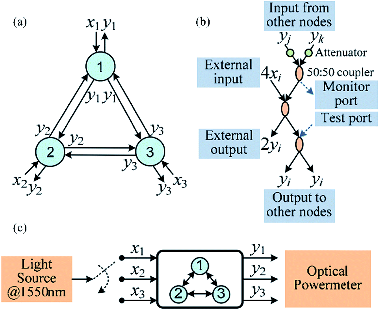 | ||
| Fig. 14 (a) Schematic of an optical matrix inversion calculator with an optical fiber network. (b) Design of a node. (c) Experimental setup. This figure has been adapted from ref. 120 with permission from Optics Express. | ||
This method can be extended to the inversion calculation of an N × N matrix with N nodes. A more convenient solution is to use silicon integrated photonics so that a compact on-chip optical network can be obtained. The nonlinear property of LDMs can form tunable attenuators on the chip to adjust the network weight in each node. The high thermo-optic effect of LDMs allows highly efficient control of the light signal.
The second demonstration is an optical solver for the NP-complete problem “Hamiltonian path”, as shown in Fig. 15.121 NP-complete problems are a set of problems with exponential calculation complexity and are widely investigated in the areas of secure communication, network traffic management, resource optimization, etc. Different NP-complete problems can be converted to each other with a polynomial algorithm. So here we focus on one NP-complete problem, the “Hamiltonian path”: for a network, if there exists a path that visits all the nodes exactly once.
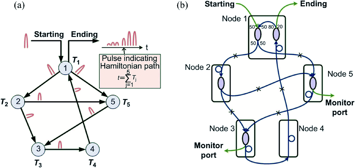 | ||
| Fig. 15 (a) Schematic of an optical solver for NP-complete problem “Hamiltonian path”. (b) Actual design of the network with optical fiber components. This figure has been adapted from ref. 121 with permission from Light: Science & Applications. | ||
The schematic diagram of the optical NP-complete problem solver is shown in Fig. 15(a). The solver consists of five nodes connected by directional optical fibers to represent a target network. Each node is assigned a specific delay Tj (j = 1–5). The delay values are designed such that their sum  is unique, i.e., can only be obtained by summing each node's delay exactly once. This network is then probed by a short optical pulse. If an output pulse with a delay equal to
 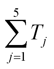 is observed, we can conclude that a Hamiltonian path exists; otherwise, the answer is negative. The actual design based on optical fibers and fiber couplers of the network is shown in Fig. 15(b). Compared with conventional computers, the solving time of this optical solver only depends on the light propagation time in the network, which can be within nanoseconds or even picoseconds. This optical method can also be extended to a large-scale network. Both fiber network and integrated photonic network can be utilized. The LDMs can function as a fast switch or a nonlinear device in the network, enabling a highly reconfigurable and diversified optical network.
Currently, there are still some challenges for the application of all-optical devices with LDMs. For example, all-optical signal processing requires highly stable devices. Current all-optical devices with LDMs are still vulnerable to environmental disturbance. The performance of all-optical devices is related to the quality of LDMs. High-yield, high-quality and repeatable fabrication of LDMs is still challenging. Large-scale applications of all-optical devices with LDMs may also require a compact size and optical integration of LDMs should be investigated.
Conclusions
In conclusion, we have reviewed the recent progress on fiber all-optical devices based on two main nonlinear mechanisms in LDMs, the thermo-optic effect and saturable absorption. The compactness of LDMs makes them the ideal medium for fiber systems. It is promising that all-optical devices can be applied to various photonic applications such as all-optical communications, optical computing, photonic artificial intelligence and optical neural networks.Conflicts of interest
There are no conflicts to declare.Acknowledgements
The research was partially supported by the National Natural Science Foundation of China (Grant No. 61435010, 61535006, 61875122, 6181101252 and 61922056) and the Science and Technology Innovation Commission of Shenzhen (KQTD2015032416270385, JCYJ20150625103619275, and JCYJ20170811093453105).Notes and references
- D. J. Richardson, J. M. Fini and L. E. Nelson, Nat. Photonics, 2013, 7, 354–362 CrossRef CAS.
- R. L. Gieseking, S. Mukhopadhyay, C. Risko, S. R. Marder and J.-L. Brédas, Adv. Mater., 2014, 26, 68–84 CrossRef CAS PubMed.
- A. E. Willner, S. Khaleghi, M. R. Chitgarha and O. F. Yilmaz, J. Lightwave Technol., 2014, 32, 660–680 Search PubMed.
- V. R. Almeida, C. A. Barrios, R. R. Panepucci and M. Lipson, Nature, 2004, 431, 1081–1084 CrossRef CAS PubMed.
- T. Volz, A. Reinhard, M. Winger, A. Badolato, K. J. Hennessy, E. L. Hu and A. Imamoğlu, Nat. Photonics, 2012, 6, 605–609 CrossRef.
- K. Nozaki, T. Tanabe, A. Shinya, S. Matsuo, T. Sato, H. Taniyama and M. Notomi, Nat. Photonics, 2010, 4, 477–483 CrossRef CAS.
- X. Hu, P. Jiang, C. Ding, H. Yang and Q. Gong, Nat. Photonics, 2008, 2, 185–189 CrossRef CAS.
- W. Li, B. Chen, C. Meng, W. Fang, Y. Xiao, X. Li, Z. Hu, Y. Xu, L. Tong and H. Wang, Nano Lett., 2014, 14, 955–959 CrossRef CAS PubMed.
- M. Liu, X. Yin, E. Ulin-Avila, B. Geng, T. Zentgraf, L. Ju, F. Wang and X. J. N. Zhang, Nature, 2011, 474, 64–67 CrossRef CAS PubMed.
- Z. Sun, A. Martinez and F. Wang, Nat. Photonics, 2016, 10, 227–238 CrossRef CAS.
- Y. Wang, W. Huang, C. Wang, J. Guo, F. Zhang, Y. Song, Y. Ge, L. Wu, J. Liu, J. Li and H. Zhang, Laser Photonics Rev., 2019, 13, 1800313 CrossRef.
- Y. Wang, W. Huang, J. Zhao, H. Huang, C. Wang, F. Zhang, J. Liu, J. Li, M. Zhang and H. Zhang, J. Mater. Chem. C, 2019, 7, 871–878 RSC.
- Y. Wang, K. Wu and J. Chen, Chin. Opt. Lett., 2018, 16, 020003 CrossRef.
- Y. Wang, F. Zhang, X. Tang, X. Chen, Y. Chen, W. Huang, Z. Liang, L. Wu, Y. Ge, Y. Song, J. Liu, D. Zhang, J. Li and H. Zhang, Laser Photonics Rev., 2018, 12, 1800016 CrossRef.
- L. Wu, X. Jiang, J. Zhao, W. Liang, Z. Li, W. Huang, Z. Lin, Y. Wang, F. Zhang, S. Lu, Y. Xiang, S. Xu, J. Li and H. Zhang, Laser Photonics Rev., 2018, 12, 1800215 CrossRef.
- Q. Wu, S. Chen, Y. Wang, L. Wu, X. Jiang, F. Zhang, X. Jin, Q. Jiang, Z. Zheng, J. Li, M. Zhang and H. Zhang, Adv. Mater., 2019, 4, 1800532 Search PubMed.
- S. Yu, X. Wu, K. Chen, B. Chen, X. Guo, D. Dai, L. Tong, W. Liu and Y. Ron Shen, Optica, 2016, 3, 541–544 CrossRef CAS.
- X. Gan, C. Zhao, Y. Wang, D. Mao, L. Fang, L. Han and J. Zhao, Optica, 2015, 2, 468–471 CrossRef CAS.
- K. Wu, C. Guo, H. Wang, X. Zhang, J. Wang and J. Chen, Opt. Express, 2017, 25, 17639–17649 CrossRef CAS PubMed.
- Q. Guo, K. Wu, Z. Shao, E. T. Basore, P. Jiang and J. Qiu, Adv. Opt. Mater., 2019, 7, 1900322 CrossRef.
- Y.-C. Chen, N. R. Raravikar, L. S. Schadler, P. M. Ajayan, Y.-P. Zhao, T.-M. Lu, G.-C. Wang and X.-C. Zhang, Appl. Phys. Lett., 2002, 81, 975–977 CrossRef CAS.
- Y. Song, Y. Chen, X. Jiang, W. Liang, K. Wang, Z. Liang, Y. Ge, F. Zhang, L. Wu, J. Zheng, J. Ji and H. Zhang, Adv. Opt. Mater., 2018, 6, 1701287 CrossRef.
- S. Tatsuura, M. Furuki, Y. Sato, I. Iwasa, M. Tian and H. Mitsu, Adv. Mater., 2003, 15, 534–537 CrossRef CAS.
- Z. Sun, T. Hasan, F. Torrisi, D. Popa, G. Privitera, F. Wang, F. Bonaccorso, D. M. Basko and A. C. Ferrari, ACS Nano, 2010, 4, 803–810 CrossRef CAS PubMed.
- A. Martinez and Z. Sun, Nat. Photonics, 2013, 7, 842–845 CrossRef CAS.
- T. Mueller, F. Xia and P. Avouris, Nat. Photonics, 2010, 4, 297–301 CrossRef CAS.
- T. Gu, N. Petrone, J. F. McMillan, A. van der Zande, M. Yu, G.-Q. Lo, D.-L. Kwong, J. Hone and C. W. Wong, Nat. Photonics, 2012, 6, 554–559 CrossRef CAS.
- D. A. Dikin, S. Stankovich, E. J. Zimney, R. D. Piner, G. H. B. Dommett, G. Evmenenko, S. T. Nguyen and R. S. Ruoff, Nature, 2007, 448, 457–460 CrossRef CAS PubMed.
- G. Sobon, J. Sotor, J. Jagiello, R. Kozinski, M. Zdrojek, M. Holdynski, P. Paletko, J. Boguslawski, L. Lipinska and K. M. Abramski, Opt. Express, 2012, 20, 19463–19473 CrossRef CAS PubMed.
- R. H. Baughman, A. A. Zakhidov and W. A. de Heer, Science, 2002, 297, 787–792 CrossRef CAS PubMed.
- F. Wang, A. G. Rozhin, V. Scardaci, Z. Sun, F. Hennrich, I. H. White, W. I. Milne and A. C. Ferrari, Nat. Nanotechnol., 2008, 3, 738–742 CrossRef CAS PubMed.
- X. Liu, D. Han, Z. Sun, C. Zeng, H. Lu, D. Mao, Y. Cui and F. Wang, Sci. Rep., 2013, 3, 2718 CrossRef PubMed.
- X. Yin, Z. Ye, D. A. Chenet, Y. Ye, K. O'Brien, J. C. Hone and X. Zhang, Science, 2014, 344, 488–490 CrossRef CAS PubMed.
- Q. H. Wang, K. Kalantar-Zadeh, A. Kis, J. N. Coleman and M. S. Strano, Nat. Nanotechnol., 2012, 7, 699–712 CrossRef CAS PubMed.
- P. Yan, A. Liu, Y. Chen, J. Wang, S. Ruan, H. Chen and J. Ding, Sci. Rep., 2015, 5, 12587 CrossRef CAS PubMed.
- J. E. Moore, Nature, 2010, 464, 194–198 CrossRef CAS PubMed.
- H. Zhang, C.-X. Liu, X.-L. Qi, X. Dai, Z. Fang and S.-C. Zhang, Nat. Phys., 2009, 5, 438–442 Search PubMed.
- J. Lee, J. Koo, Y. M. Jhon and J. H. Lee, Opt. Express, 2014, 22, 6165–6173 CrossRef CAS PubMed.
- F. Xia, H. Wang and Y. Jia, Nat. Commun., 2014, 5, 4458 CrossRef CAS PubMed.
- N. Youngblood, C. Chen, S. J. Koester and M. Li, Nat. Photonics, 2015, 9, 247–252 CrossRef CAS.
- H. Yuan, X. Liu, F. Afshinmanesh, W. Li, G. Xu, J. Sun, B. Lian, A. G. Curto, G. Ye, Y. Hikita, Z. Shen, S.-C. Zhang, X. Chen, M. Brongersma, H. Y. Hwang and Y. Cui, Nat. Nanotechnol., 2015, 10, 707–713 CrossRef CAS PubMed.
- X. Wang, S. Kajiyama, H. Iinuma, E. Hosono, S. Oro, I. Moriguchi, M. Okubo and A. Yamada, Nat. Commun., 2015, 6, 6544 CrossRef CAS PubMed.
- X. Jiang, S. Liu, W. Liang, S. Luo, Z. He, Y. Ge, H. Wang, R. Cao, F. Zhang, Q. Wen, J. Li, Q. Bao, D. Fan and H. Zhang, Laser Photonics Rev., 2018, 12, 1700229 CrossRef.
- L. Cheng, J. Liu, X. Gu, H. Gong, X. Shi, T. Liu, C. Wang, X. Wang, G. Liu, H. Xing, W. Bu, B. Sun and Z. Liu, Adv. Mater., 2014, 26, 1886–1893 CrossRef CAS PubMed.
- M. Chen, S. Tang, Z. Guo, X. Wang, S. Mo, X. Huang, G. Liu and N. Zheng, Adv. Mater., 2014, 26, 8210–8216 CrossRef CAS PubMed.
- P. Yan, H. Chen, J. Yin, Z. Xu, J. Li, Z. Jiang, W. Zhang, J. Wang, I. L. Li and Z. Sun, Nanoscale, 2017, 9, 1871–1877 RSC.
- T. Hasan, Z. Sun, F. Wang, F. Bonaccorso, P. H. Tan, A. G. Rozhin and A. C. Ferrari, Adv. Mater., 2009, 21, 3874–3899 CrossRef CAS.
- Q. Bao, H. Zhang, J. x. Yang, S. Wang, D. Y. Tang, R. Jose, S. Ramakrishna, C. T. Lim and K. P. Loh, Adv. Funct. Mater., 2010, 20, 782–791 CrossRef CAS.
- S. Cui, H. Pu, S. A. Wells, Z. Wen, S. Mao, J. Chang, M. C. Hersam and J. Chen, Nat. Commun., 2015, 6, 8632 CrossRef CAS PubMed.
- D. J. Lipomi, M. Vosgueritchian, B. C. K. Tee, S. L. Hellstrom, J. A. Lee, C. H. Fox and Z. Bao, Nat. Nanotechnol., 2011, 6, 788–792 CrossRef CAS PubMed.
- Q. He, S. Wu, Z. Yin and H. Zhang, Chem. Sci., 2012, 3, 1764–1772 RSC.
- B. Anasori, M. R. Lukatskaya and Y. Gogotsi, Nat. Rev. Mater., 2017, 2, 16098 CrossRef CAS.
- Y. Dong, Z.-S. Wu, W. Ren, H.-M. Cheng and X. Bao, Sci. Bull., 2017, 62, 724–740 CrossRef CAS.
- C. Wu, X. Lu, L. Peng, K. Xu, X. Peng, J. Huang, G. Yu and Y. Xie, Nat. Commun., 2013, 4, 2431 CrossRef PubMed.
- Q. Qu, S. Yang and X. Feng, Adv. Mater., 2011, 23, 5574–5580 CrossRef CAS PubMed.
- L. Liao, Y.-C. Lin, M. Bao, R. Cheng, J. Bai, Y. Liu, Y. Qu, K. L. Wang, Y. Huang and X. Duan, Nature, 2010, 467, 305–308 CrossRef CAS PubMed.
- K. Roy, M. Padmanabhan, S. Goswami, T. P. Sai, G. Ramalingam, S. Raghavan and A. Ghosh, Nat. Nanotechnol., 2013, 8, 826–830 CrossRef CAS PubMed.
- Z. Luo, D. Wu, B. Xu, H. Xu, Z. Cai, J. Peng, J. Weng, S. Xu, C. Zhu and F. Wang, Nanoscale, 2016, 8, 1066–1072 RSC.
- W. Liu, L. Pang, H. Han, W. Tian, H. Chen, M. Lei, P. Yan and Z. Wei, Sci. Rep., 2016, 6, 19997 CrossRef PubMed.
- J. Li, H. Luo, B. Zhai, R. Lu, Z. Guo, H. Zhang and Y. Liu, Sci. Rep., 2016, 6, 30361 CrossRef CAS PubMed.
- Y. I. Jhon, J. Koo, B. Anasori, M. Seo, J. H. Lee, Y. Gogotsi and Y. M. Jhon, Adv. Mater., 2017, 29, 1702496 CrossRef PubMed.
- P. Xiao, K. Wu, D. Mao and J. Chen, Opt. Express, 2019, 27, 4188–4203 CrossRef CAS PubMed.
- O. Lopez-Sanchez, D. Lembke, M. Kayci, A. Radenovic and A. Kis, Nat. Nanotechnol., 2013, 8, 497–501 CrossRef CAS PubMed.
- W. Zheng, T. Xie, Y. Zhou, Y. L. Chen, W. Jiang, S. Zhao, J. Wu, Y. Jing, Y. Wu, G. Chen, Y. Guo, J. Yin, S. Huang, H. Q. Xu, Z. Liu and H. Peng, Nat. Commun., 2015, 6, 6972 CrossRef CAS PubMed.
- Y. Ge, Z. Zhu, Y. Xu, Y. Chen, S. Chen, Z. Liang, Y. Song, Y. Zou, H. Zeng, S. Xu, H. Zhang and D. Fan, Adv. Opt. Mater., 2018, 6, 1701166 CrossRef.
- Y. Song, Z. Liang, X. Jiang, Y. Chen, Z. Li, L. Lu, Y. Ge, K. Wang, J. Zheng, S. Lu, J. Ji and H. Zhang, 2D Mater., 2017, 4, 045010 CrossRef.
- C. Wang, Y. Wang, X. Jiang, J. Xu, W. Huang, F. Zhang, J. Liu, F. Yang, Y. Song, Y. Ge, Q. Wu, M. Zhang, H. Chen, J. Liu and H. Zhang, Adv. Opt. Mater., 2019, 7, 1900060 CrossRef.
- J. Zheng, X. Tang, Z. Yang, Z. Liang, Y. Chen, K. Wang, Y. Song, Y. Zhang, J. Ji, Y. Liu, D. Fan and H. Zhang, Adv. Opt. Mater., 2017, 5, 1700026 CrossRef.
- F. Xia, H. Wang, D. Xiao, M. Dubey and A. Ramasubramaniam, Nat. Photonics, 2014, 8, 899–907 CrossRef CAS.
- R. R. Nair, P. Blake, A. N. Grigorenko, K. S. Novoselov, T. J. Booth, T. Stauber, N. M. R. Peres and A. K. Geim, Science, 2008, 320, 1308 CrossRef CAS PubMed.
- F. Xia, T. Mueller, Y.-m. Lin, A. Valdes-Garcia and P. Avouris, Nat. Nanotechnol., 2009, 4, 839–843 CrossRef CAS PubMed.
- J. Tarka, G. Sobon, J. Boguslawski, J. Sotor, J. Jagiello, M. Aksienionek, L. Lipinska, M. Zdrojek, J. Judek and K. M. Abramski, Opt. Mater. Express, 2014, 4, 1981–1986 CrossRef.
- E. Pop, V. Varshney and A. K. Roy, MRS Bull., 2012, 37, 1273–1281 CrossRef CAS.
- R. Li, L. Zhang, L. Shi and P. Wang, ACS Nano, 2017, 11, 3752–3759 CrossRef CAS PubMed.
- M. Naguib, J. Come, B. Dyatkin, V. Presser, P.-L. Taberna, P. Simon, M. W. Barsoum and Y. Gogotsi, Electrochem. Commun., 2012, 16, 61–64 CrossRef CAS.
- K. J. Koski, C. D. Wessells, B. W. Reed, J. J. Cha, D. Kong and Y. Cui, J. Am. Chem. Soc., 2012, 134, 13773–13779 CrossRef CAS PubMed.
- C.-Z. Chang, P. Tang, X. Feng, K. Li, X.-C. Ma, W. Duan, K. He and Q.-K. Xue, Phys. Rev. Lett., 2015, 115, 136801 CrossRef PubMed.
- J. Zhang, C.-Z. Chang, Z. Zhang, J. Wen, X. Feng, K. Li, M. Liu, K. He, L. Wang, X. Chen, Q.-K. Xue, X. Ma and Y. Wang, Nat. Commun., 2011, 2, 574 CrossRef PubMed.
- Y. Zhang, K. He, C.-Z. Chang, C.-L. Song, L.-L. Wang, X. Chen, J.-F. Jia, Z. Fang, X. Dai, W.-Y. Shan, S.-Q. Shen, Q. Niu, X.-L. Qi, S.-C. Zhang, X.-C. Ma and Q.-K. Xue, Nat. Phys., 2010, 6, 584–588 Search PubMed.
- J. Du, M. Zhang, Z. Guo, J. Chen, X. Zhu, G. Hu, P. Peng, Z. Zheng and H. Zhang, Sci. Rep., 2017, 7, 42357 Search PubMed.
- X. Wang and S. Lan, Adv. Opt. Photonics, 2016, 8, 618–655 Search PubMed.
- L. Lu, Z. Liang, L. Wu, Y. Chen, Y. Song, S. C. Dhanabalan, J. S. Ponraj, B. Dong, Y. Xiang, F. Xing, D. Fan and H. Zhang, Laser Photonics Rev., 2018, 12, 1700221 Search PubMed.
- W. Tao, X. Ji, X. Xu, M. A. Islam, Z. Li, S. Chen, P. E. Saw, H. Zhang, Z. Bharwani, Z. Guo, J. Shi and O. C. Farokhzad, Angew. Chem., Int. Ed., 2017, 56, 11896–11900 CrossRef CAS PubMed.
- S. Y. Set, H. Yaguchi, Y. Tanaka and M. Jablonski, J. Lightwave Technol., 2004, 22, 51 CrossRef CAS.
- H. Xia, H. Li, C. Lan, C. Li, X. Zhang, S. Zhang and Y. Liu, Opt. Express, 2014, 22, 17341–17348 CrossRef PubMed.
- A. Reina, X. Jia, J. Ho, D. Nezich, H. Son, V. Bulovic, M. S. Dresselhaus and J. Kong, Nano Lett., 2009, 9, 30–35 CrossRef CAS PubMed.
- K. S. Novoselov, A. K. Geim, S. V. Morozov, D. Jiang, Y. Zhang, S. V. Dubonos, I. V. Grigorieva and A. A. Firsov, Science, 2004, 306, 666–669 CrossRef CAS PubMed.
- J. Lee, J. Koo, Y. M. Jhon and J. H. Lee, Opt. Express, 2014, 22, 6165–6173 CrossRef CAS PubMed.
- J. Sotor, G. Sobon and K. M. Abramski, Opt. Express, 2014, 22, 13244–13249 CrossRef CAS PubMed.
- J. Sotor, G. Sobon, W. Macherzynski and K. M. Abramski, Laser Phys. Lett., 2014, 11, 055102 CrossRef.
- H. Li, G. Lu, Y. Wang, Z. Yin, C. Cong, Q. He, L. Wang, F. Ding, T. Yu and H. Zhang, Small, 2013, 9, 1974–1981 CrossRef CAS PubMed.
- E. Aharon, A. Albo, M. Kalina and G. L. Frey, Adv. Funct. Mater., 2006, 16, 980–986 CrossRef CAS.
- Z. Zeng, Z. Yin, X. Huang, H. Li, Q. He, G. Lu, F. Boey and H. Zhang, Angew. Chem., Int. Ed., 2011, 50, 11093–11097 CrossRef CAS PubMed.
- Y. Hernandez, V. Nicolosi, M. Lotya, F. M. Blighe, Z. Sun, S. De, I. T. McGovern, B. Holland, M. Byrne, Y. K. Gun'Ko, J. J. Boland, P. Niraj, G. Duesberg, S. Krishnamurthy, R. Goodhue, J. Hutchison, V. Scardaci, A. C. Ferrari and J. N. Coleman, Nat. Nanotechnol., 2008, 3, 563–568 CrossRef CAS PubMed.
- Y. Wang, X. Gan, C. Zhao, L. Fang, D. Mao, Y. Xu, F. Zhang, T. Xi, L. Ren and J. Zhao, Appl. Phys. Lett., 2016, 108, 171905 CrossRef.
- K. Wu, Y. Wang, C. Qiu and J. Chen, Photonics Res., 2018, 6, C22–C28 CrossRef CAS.
- J. Liu, J. Liu, Z. Guo, H. Zhang, W. Ma, J. Wang and L. Su, Opt. Express, 2016, 24, 30289–30295 CrossRef CAS PubMed.
- P. Li, Y. Chen, T. Yang, Z. Wang, H. Lin, Y. Xu, L. Li, H. Mu, B. N. Shivananju, Y. Zhang, Q. Zhang, A. Pan, S. Li, D. Tang, B. Jia, H. Zhang and Q. Bao, ACS Appl. Mater. Interfaces, 2017, 9, 12759–12765 CrossRef CAS PubMed.
- Z. Liu, H. Mu, S. Xiao, R. Wang, Z. Wang, W. Wang, Y. Wang, X. Zhu, K. Lu, H. Zhang, S. T. Lee, Q. Bao and W. Ma, Adv. Mater., 2016, 28, 3535–3542 CrossRef CAS PubMed.
- Y. F. Song, H. Zhang, D. Y. Tang and D. Y. Shen, Opt. Express, 2012, 20, 27283–27289 CrossRef CAS PubMed.
- Z. Wang, Y. Xu, S. C. Dhanabalan, J. Sophia, C. Zhao, C. Xu, Y. Xiang, J. Li and H. Zhang, IEEE Photonics J., 2016, 8, 1–10 Search PubMed.
- Y. Xu, X.-F. Jiang, Y. Ge, Z. Guo, Z. Zeng, Q.-H. Xu, H. Zhang, X.-F. Yu and D. Fan, J. Mater. Chem. C, 2017, 5, 3007–3013 RSC.
- Y. Song, S. Chen, Q. Zhang, L. Li, L. Zhao, H. Zhang and D. Tang, Opt. Express, 2016, 24, 25933–25942 CrossRef CAS PubMed.
- G. Zheng, Y. Chen, H. Huang, C. Zhao, S. Lu, S. Chen, H. Zhang and S. Wen, ACS Appl. Mater. Interfaces, 2013, 5, 10288–10293 CrossRef CAS PubMed.
- Q. Wang, Y. Chen, G. Jiang, L. Miao, C. Zhao, X. Fu, S. Wen and H. Zhang, IEEE Photonics J., 2015, 7, 1–11 Search PubMed.
- M. M. Fejer, G. A. Magel, D. H. Jundt and R. L. Byer, IEEE J. Quantum Electron., 1992, 28, 2631–2654 CrossRef.
- D. J. Bradley and G. H. C. New, Proc. IEEE, 1974, 62, 313–345 Search PubMed.
- J. Chen, W. Xia and M. Wang, J. Appl. Phys., 2017, 121, 223103 CrossRef.
- A. Hayat, A. Nevet, P. Ginzburg and M. Orenstein, Semicond. Sci. Technol., 2011, 26, 083001 CrossRef.
- J. K. Ranka, A. L. Gaeta, A. Baltuska, M. S. Pshenichnikov and D. A. Wiersma, Opt. Lett., 1997, 22, 1344–1346 CrossRef CAS PubMed.
- D. Reid, W. Sibbett, J. Dudley, L. Barry, B. Thomsen and J. Harvey, Appl. Opt., 1998, 37, 8142–8144 CrossRef CAS.
- G. Cong, M. Okano, Y. Maegami, M. Ohno and K. Yamada, Opt. Express, 2018, 26, 15090–15100 CrossRef CAS PubMed.
- A. Smolyaninov, M.-H. Yang, L. Pang and Y. Fainman, Opt. Lett., 2016, 41, 4445–4448 CrossRef CAS PubMed.
- G. R. Bhimanapati, Z. Lin, V. Meunier, Y. Jung, J. Cha, S. Das, D. Xiao, Y. Son, M. S. Strano, V. R. Cooper, L. Liang, S. G. Louie, E. Ringe, W. Zhou, S. S. Kim, R. R. Naik, B. G. Sumpter, H. Terrones, F. Xia, Y. Wang, J. Zhu, D. Akinwande, N. Alem, J. A. Schuller, R. E. Schaak, M. Terrones and J. A. Robinson, ACS Nano, 2015, 9, 11509–11539 CrossRef CAS PubMed.
- H. Rajbenbach, Y. Fainman and S. H. Lee, Appl. Opt., 1987, 26, 1024–1031 CrossRef CAS PubMed.
- J. L. O'Brien, Science, 2007, 318, 1567–1570 CrossRef PubMed.
- H. J. Caulfield and S. Dolev, Nat. Photonics, 2010, 4, 261–263 CrossRef CAS.
- L. Appeltant, M. C. Soriano, G. Van der Sande, J. Danckaert, S. Massar, J. Dambre, B. Schrauwen, C. R. Mirasso and I. Fischer, Nat. Commun., 2011, 2, 468 CrossRef CAS PubMed.
- D. Woods and T. J. Naughton, Nat. Phys., 2012, 8, 257–259 Search PubMed.
- K. Wu, C. Soci, P. P. Shum and N. I. Zheludev, Opt. Express, 2014, 22, 295–304 CrossRef PubMed.
- K. Wu, J. García de Abajo, C. Soci, P. Ping Shum and N. I. Zheludev, Light: Sci. Appl., 2014, 3, e147 CrossRef CAS.
Footnote |
| † These authors contributed equally. |
| This journal is © The Royal Society of Chemistry 2019 |