
 Open Access Article
 This Open Access Article is licensed under a Creative Commons Attribution-Non Commercial 3.0 Unported Licence
Quantum dot based 3D printed woodpile photonic crystals tuned for the visible†
Ioanna
Sakellari
 *a,
Elmina
Kabouraki
ab,
Dimitris
Karanikolopoulos
a,
Sotiris
Droulias
*a,
Maria
Farsari
a,
Panagiotis
Loukakos
a,
Maria
Vamvakaki
ab and
David
Gray
a
*a,
Elmina
Kabouraki
ab,
Dimitris
Karanikolopoulos
a,
Sotiris
Droulias
*a,
Maria
Farsari
a,
Panagiotis
Loukakos
a,
Maria
Vamvakaki
ab and
David
Gray
a
aInstitute of Electronic Structure and Laser, FORTH, 71110 Heraklion, Crete, Greece. E-mail: isakel@iesl.forth.gr; sdroulias@iesl.forth.gr
bDepartment of Materials Science and Technology, University of Crete, Heraklion, Crete, Greece
First published on 9th July 2019
Abstract
The development of dynamically responsive 3D photonic elements, which is crucial for the design of active integrated photonic circuits, requires the incorporation of material systems with fast and tunable response. To this end, semiconductor quantum dots have been widely used to perform as the active material system to be integrated; nonetheless, multiple-step processing is usually required for the active functions to be preserved, thereby restricting functionality of integrated 3D quantum photonic elements mostly to the infrared. Here, we report a simple scheme for the realization of visible light active 3D photonic devices by combining direct laser writing with two-photon absorption and in situ synthesis of cadmium sulfide (CdS) nanoparticles. The novel active 3D printable hybrid material is synthesized by crosslinking precursors of CdS quantum dots into a photo-structurable organic–inorganic zirconium–silicon hybrid composite integrating functional properties of both high spatial resolution and high third-order nonlinearity into the photonic matrix. As a proof-of-demonstration for 3D printed active photonic devices, woodpile photonic crystals with an inlayer periodicity down to 500 nm are successfully fabricated showing clear photonic stop bands in the visible spectral region, while for the first time, evidence of an ultrafast dynamic response in the visible is also demonstrated.
Introduction
The design of responsive materials for dynamic tuning of photonic properties has been a subject of intense research in the last decades because of possible applications for all optical switching devices in active photonic integrated circuits. A significant modification of the light–matter interaction can be achieved, for example, by the incorporation of quantum dot (QD) semiconductor nanoparticles in a photonic polymer matrix, where the energy of band-to-band transitions in the embedded nanoparticles can be designed to overlap with the photonic-band-gap region.1,2 Composites consisting of nano-sized particles incorporated in a polymer matrix are of great interest due to their long-term stability offering new strategies for influencing interactions that may take place between the matrix and the QDs. These composites are promising materials for a new generation of optical and electronic devices, as well as for biological labelling.3–5One way to implement an all-optical switching photonic device is based on a Kerr-type nonlinearity, that is, the refractive index of one of the materials embedded in the photonic matrix depends on the local intensity of light and, hence, the photonic-band-gap material exhibits a band structure that changes dynamically with light. Thus, the position of the photonic-band-gap can be dynamically tuned and the overall transmittance can be subsequently adjusted to be either high (“on” state) or low (“off” state). In order to achieve high intensity contrast between “on” and “off” states of the optical switch, a high nonlinear Kerr coefficient is required along with a narrow resonance of the photonic switch. In addition, a well confined light emitter in 3D is also highly desirable for complete control over the photonic density of states. Nanocrystal QDs are very well known for their large third-order (Kerr-type) non-linearity arising from the quantum size effect.6 Due to the existence of a complete photonic-band-gap,7–9 3D photonic crystals provide a unique tailored dielectric platform in which the active properties of embedded sources can be well controlled.
Although many novel photonic devices comprising 3D photonic crystals have been previously proposed,10 (e.g., opals, inverse opals, woodpile) it has been a challenge to experimentally incorporate QDs into 3D photonic crystal lattices and realize devices with demonstrable functionalities on the basis of single-step processing with the ability to preserve the active material properties. Self-assembly11 and inversion12 methods in combination with post-fabrication infiltration,13 as well as patterning polymeric materials with embedded QDs using layer by layer lithography14 are nowadays the main approaches to QD containing 3D periodic structures. Furthermore, the development of novel active 3D optical elements by direct patterning has been restricted mostly to the IR as QD structuring cannot reach optical-grade quality in the visible, since the dimensions of the features should be approximately λ/4n (λ, wavelength and n, the refractive index).
On the other hand, optical lithography via direct laser writing (DLW) fabrication15 brings the flexibility to engineer a variety of different lattice arrangements, which makes it an excellent candidate for the fabrication of intrinsic 3D devices, such as 3D photonic crystals. Several efforts have been undertaken in order to improve the resolution of direct laser written structures at the nanometer scale,16–18 as well as to realize functional 3D microstructures by incorporating nanocrystal QDs in the polymer resin.19–26 In DLW, usually QDs are either combined with pure organic materials lacking structural stability due to shrinkage22,23,26,27 and, hence, restricting functionality mostly to the IR region, or they are dispersed in commercially available photoresists that wash out during the development process as they are not part of the photopolymer.19,24,25 In addition, segregation of the QDs during polymerization causes the photosensitive resin to become opaque, thus eliminating the possibility to fabricate 3D microstructures.24,25 Nevertheless, these common QDs related phenomena can be overcome by their appropriate functionalization.20,22
In the present work, in order to avoid absorption and scattering due to QD aggregation, we choose in situ synthesis of semiconductor QDs within the 3D polymer photonic matrix after DLW fabrication by polymerizing appropriate QD precursor molecules in a photo-patternable polymer resin. The latter is an organic–inorganic hybrid composite material that is synthesized via the sol–gel process,28 a versatile technique that has been exploited for the incorporation of inorganic networks into polymer matrices using as monomers molecules that carry an inorganic moiety and a polymerizable organic group. The former serves as the precursor to the inorganic network, whereas the latter acts as the precursor to the organic polymer. Thus, by choosing from an enormous variety of precursor molecules, this technique offers the possibility to alter the composite material properties. The novel active photo-structurable material presented herein allows, on one hand, the homogeneous incorporation of QDs in a crosslinked polymer matrix and, on the other, combines the properties of its constituent components enabling the fabrication of 3D active devices on a smaller scale exhibiting low shrinkage and high spatial resolution.16,27,29
Therefore, of direct relevance to the implementation of an all-optical switching photonic device, we show here how the two-in-one functional properties of a novel active 3D printable hybrid material – namely high spatial resolution and high χ(3) nonlinear response, can be effectively utilized, firstly, to realize the visible light photonic-band-gap properties of 3D woodpile photonic devices, and secondly, to demonstrate, for the first time, evidence of ultrafast dynamic tuning of the photonic-band-gap properties in the visible.
Results and discussion
Material synthesis and characterization
The CdS QDs were synthesized according to a modified procedure adapted from that previously reported by Z. B. Sun et al.,22,23 where the designed photo-polymerizable resin was composed of precursors of CdS QDs along with monomers and oligomers, the photoinitiator and the photosensitizer. In particular, in ref. 22 and 23, the precursors employed for the formation of CdS QDs were cadmium methacrylates (Cd(MA)2), which also served as monomers for the photo-polymerization. In the present work, Cd(MA)2 was combined with an organic–inorganic zirconium–silicon (Zr–Si) hybrid composite27 doped with the quencher 2-(dimethylamino) ethyl methacrylate (DMAEMA).16,30–32 The quencher DMAEMA, which is also a photo-polymerized monomer, offers the possibility for resolution enhancement in direct laser written structures by exploiting its free diffusion in the scanned area. This mobile quencher molecule enables the depletion of the multiphoton-generated radicals in the scanned area, as it can freely diffuse, leading to resolution improvement without compromising the mechanical stability of the structures, as it becomes part of the polymer backbone only upon irradiation. In fact, in 2012, it was demonstrated that by employing diffusion-assisted DLW,30 woodpile photonic crystals with inlayer periodicity as low as 400 nm were successfully fabricated.16 The precursor molecules employed for the synthesis of the novel photosensitive hybrid material are displayed in Fig. 1(a). Details about the preparation of the hybrid composite are provided in the Experimental section.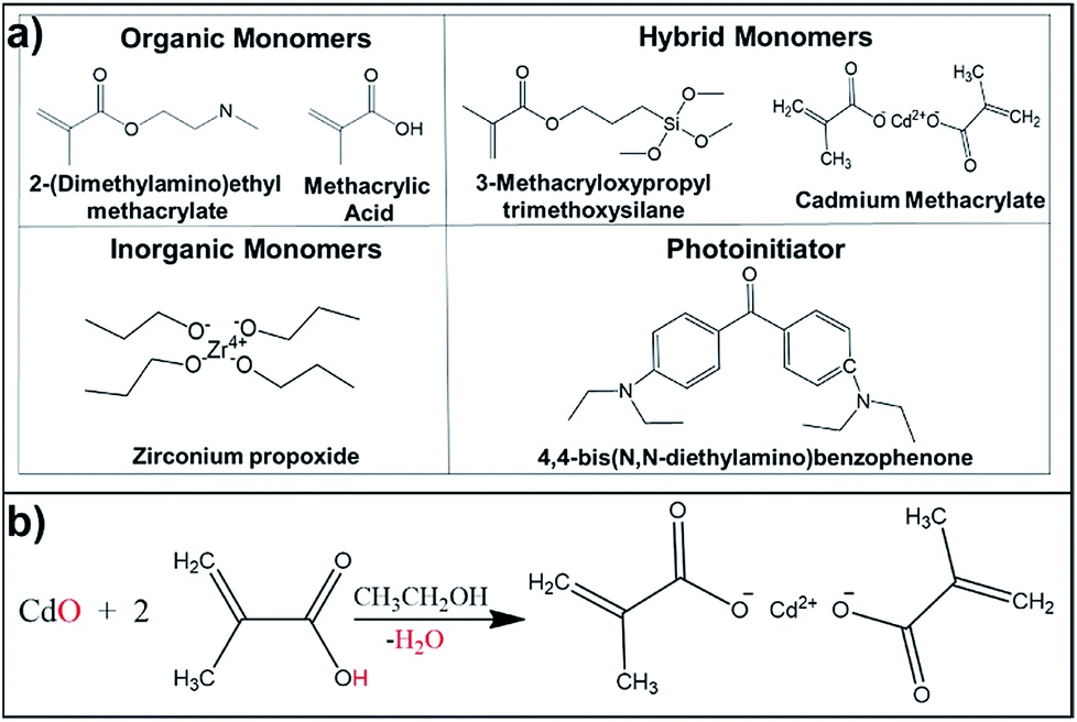 | ||
| Fig. 1 (a) Chemical formulas of the precursor molecules employed for the synthesis of the photosensitive hybrid material, (b) synthetic route of cadmium methacrylate. | ||
In our case, Cd(MA)2 was formed by mixing cadmium oxide (CdO) powder with methacrylic acid (MAA) and ethanol at room temperature (Fig. 1(b)), while CdS QDs were synthesized in the photo-polymerized polymer matrix via the reaction between the cadmium ions (Cd2+) in the polymer and sodium sulphide (Na2S). The pure polymer film containing Cd2+ (Film w/o QDs) was colorless and transparent before treatment with Na2S (Fig. 2). After a 6 hours treatment with Na2S, a broad exciton absorption band from the CdS QD appeared in the film (Film w/QDs) and demonstrated as a pale yellow nanocomposite (Fig. 2). The size of the CdS QDs was calculated to be ∼4 nm by using the Moffitt and Eisenberg formula33 along with the value of the absorption onset (i.e., 450 nm) in the respective absorption spectrum obtained by UV-Vis spectroscopy (Fig. 2).34 Also, in order to verify the formation of the CdS QDs in the polymer film, XRD measurements were performed and are provided in the ESI, Fig. S1.†
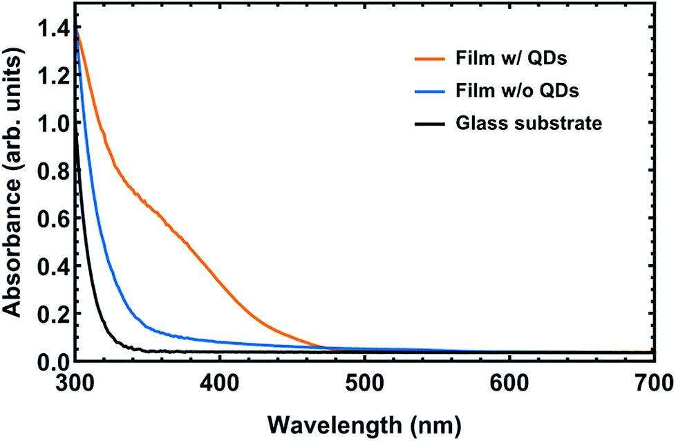 | ||
| Fig. 2 UV-Vis absorption spectra measured from a polymeric film before (blue) and after (orange) in situ synthesis of CdS quantum dots (QDs). Black line represents absorption measured from the glass substrate. | ||
The incorporation of CdS QDs in the polymer matrix results in a novel composite material that exhibits a nonlinear refractive index value of n2 = 185.7 × 10⁻¹⁵ (cm2 W−1) measured by means of the Z-scan method.35 The corresponding Z-scan measurements performed on a thin film of the QD containing material revealed the characteristic peak-valley trace of a χ(3) nonlinear material shown in Fig. 3. In particular, a positive nonlinearity is attributed to it since the peak-to-valley sequence was recorded as the sample translated towards the focusing lens. It is worth noting that the magnitude of n2 measured for the novel nanocomposite presented here is three orders of magnitude larger than those obtained for standard solvents. Such large nonlinearities have been previously reported in analogous experiments involving QDs doped nanocomposites.19,36,37
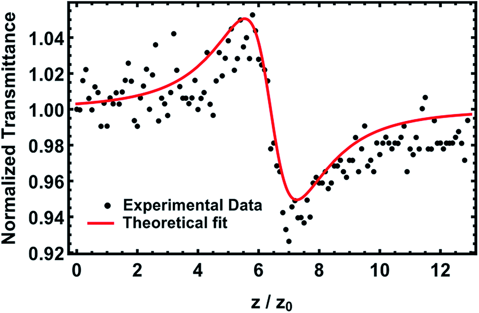 | ||
| Fig. 3 Normalized Z-scan transmittance measured at 800 nm for a polymeric film doped with CdS quantum dots. The red solid line represents the fitting used to extract the n2 value. (z0 is the Rayleigh range). | ||
Microstructure fabrication and optical characterization
Fig. 4(a) displays an optical microscopy image of an array of woodpile photonic structures fabricated by DLW functionalized with CdS QDs. The array consists of woodpile photonic crystals with a varying inlayer periodicity, α, from 600 nm (top row), to 550 nm (middle row) and, finally, to 500 nm (bottom row) with decreasing laser writing power from left to right at an energy step of ∼0.04 TW cm−2 (peak intensity at the focal point). Each woodpile structure has a footprint of 20 μm × 20 μm and consists of 10 unit cells. Fig. 4(b)–(d) display scanning electron microscopy (SEM) images of a woodpile photonic structure with an inlayer periodicity α = 500 nm functionalized with CdS QDs. The top view and side view image (Fig. 4(b) and (c), respectively), as well as a top view at higher magnification (Fig. 4(d)) demonstrate the excellent structural quality of the fabricated structures. As shown in Fig. 4(d), the QD formation procedure is not destructive for the fabricated photonic devices. Energy Dispersive X-ray Spectroscopy (EDS) measurements obtained from the functionalized woodpile structures revealed the cadmium and sulfur elements indicating the formation of the QDs within the polymer photonic matrix (ESI, Fig. S2†). The woodpile photonic crystal is designed to have a band gap along the stacking direction38 (i.e., normal to the substrate) and, hence, those structures with a prominent band gap display a vivid color as the incident light is partially reflected by the structure due to the photonic-band-gap effect (e.g., all the structures depicted on and above the main diagonal of Fig. 4(a)). In contrast, those structures not behaving as photonic-band-gap materials display a dull color as the incident light is fully transmitted (e.g., all the structures shown below the main diagonal of Fig. 4(a)).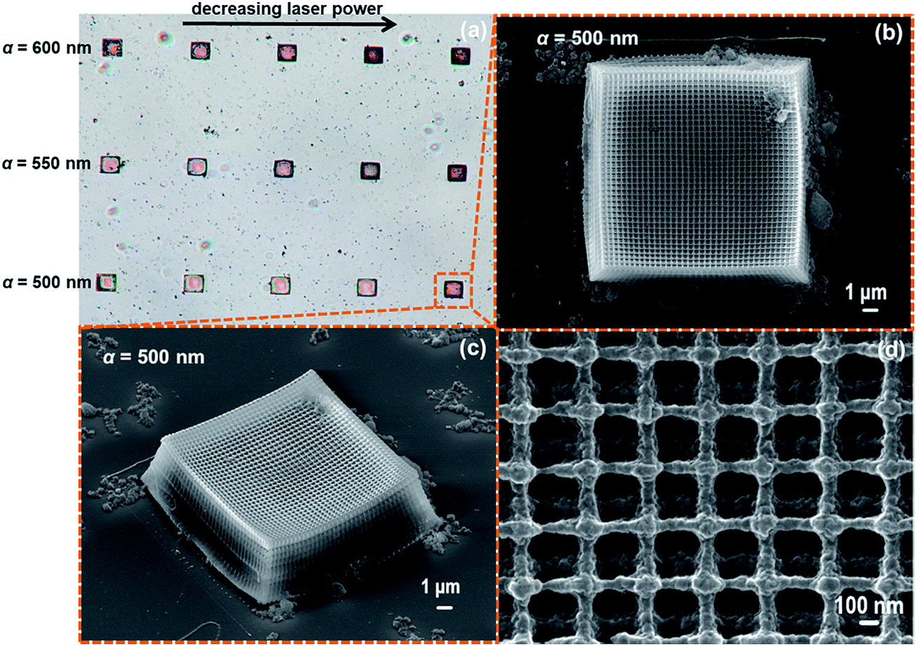 | ||
| Fig. 4 (a) Optical microscopy image of an array of woodpile photonic structures functionalized with CdS quantum dots with varying inlayer periodicity, α; 600 nm (top row), 550 nm (middle row) and 500 nm (bottom row). The laser writing power decreases from left to right, (b) SEM image of a woodpile structure with 500 nm inlayer periodicity (top view), (c) side view of (b), and (d) top view of (b) at higher magnification. | ||
The high quality of the fabricated 3D woodpile photonic crystals was further validated by the stop gaps observed in the transmission and reflection spectra shown in Fig. 5. In particular, transmission and reflection spectra were recorded before (Fig. 5(a)) and after (Fig. 5(b)) the QD formation on the 3D photonic matrix. The measurements were carried out at normal incidence (i.e., along the stacking direction of the woodpile structure) in the wavelength region from 1000 nm to 440 nm. As shown, the corresponding fundamental stop band for the case of a woodpile structure with inlayer periodicity 600 nm, 550 nm and 500 nm is clearly visible as a pronounced dip in the transmission and a peak in reflection; the central wavelength of the band gap blue shifts from 760 nm, to 710 nm, and then to 620 nm respectively. The observed photonic-band-gaps are typical to systems with weak refractive index contrast between the material of the woodpile matrix (n = 1.52) and air, when implemented with the powerful DLW technique.18,21
 | ||
| Fig. 5 Measured transmission (solid) and reflection (dashed-dot) response of woodpile photonic structures with 600 nm (red), 550 nm (black) and 500 nm (green) inlayer periodicity (a) before and (b) after in situ synthesis of CdS quantum dots (QDs). | ||
Theoretical photonic band structure calculations along the stacking direction (ΓZ) performed for the case of a woodpile structure with an inlayer periodicity α = 600 nm (shown in Fig. 6(a)) predict that the central wavelength of the fundamental stop band should lie near 960 nm, which is about 200 nm red-shifted in relation to the one experimentally observed (i.e., stop band at 760 nm). However, shrinkage effects due to excess loading of the composite material with organic molecules such as DMAEMA, resulted in the deformation of the initial structure,27 also clearly seen in the SEM images. Simulations on linear transmission spectra along the ΓZ direction, performed for the same system, are depicted in Fig. 6(b) (upper panel). It was calculated that when introducing a 20% shrinkage compared to the ideal structure (based on the SEM images) a blue-shift of the fundamental stop band of about 200 nm (Fig. 6(b), middle panel) is observed, which is in accordance with the experimental findings (i.e., stop band at 760 nm, shown in Fig. 5(a), red-colored spectra). Furthermore, sample imperfections have a direct influence on the optical properties, resulting in a less pronounced photonic-band-gap and an overall lower transmittance of about 50% in relation to the theoretically calculated value. A more pronounced effect is also observed for the peak reflectance, which is especially influenced by the surface quality.39,40 In addition, the long-wavelength band gap edge in transmission appears steeper than the short-wavelength one, the latter showing an incomplete recovery of the transmittance (see Fig. 5). In order to take into account light scattering originating from surface roughness and sample imperfections, a phenomenological imaginary part of the index of refraction for the rod permittivity was introduced in the theoretical calculations as proposed in ref. 39. The results are displayed in Fig. 6(b) (lower panel) showing good agreement with the experimental findings.
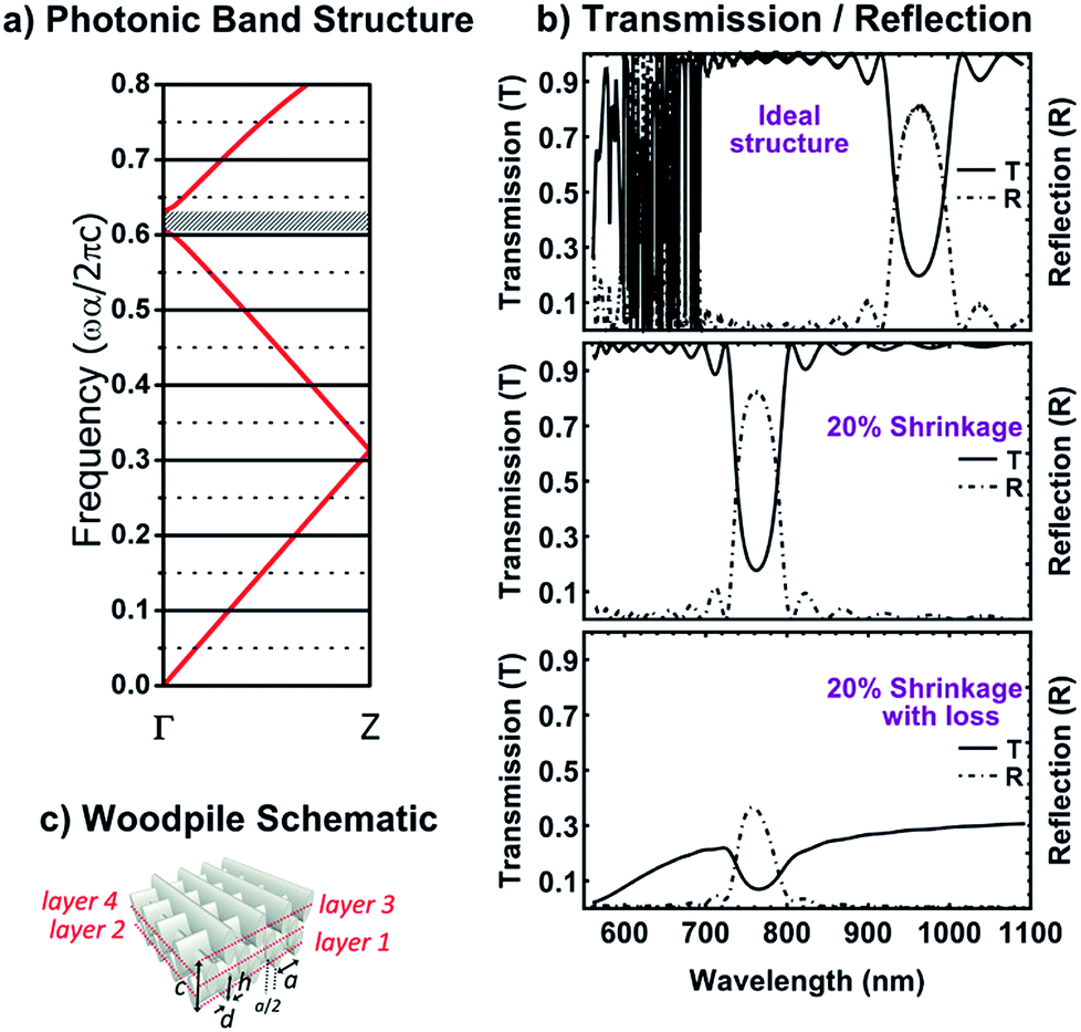 | ||
| Fig. 6 Theoretical calculations along the stacking direction (ΓZ) of a woodpile photonic crystal with an inlayer periodicity α = 600 nm: (a) photonic band structure calculations of infinite system, (b) simulated transmission (solid) and reflection (dashed-dot) response for finite system with 10 unit cells (4 × 10 = 40 layers), which is assumed to be infinite in the inlayer plane; (i) ideal structure (upper panel), (ii) introducing 20% shrinkage to the ideal structure (middle panel), (iii) introducing artificial loss (conductivity, σ) into the dielectric rods of the shrunken structure equal to σ = 3 × 10³ S (lower panel), and (c) schematic of the woodpile photonic crystal showing one unit cell (of length c) along the stacking direction. | ||
Surprisingly, in Fig. 5(b), apart from the photonic-band-gaps that are still clearly present after the QD formation on the woodpile structures, an extinction feature is also observed both in the transmission and in the reflection measurements near 550 nm for all structures, which is attributed to the formation of the CdS QDs and visualized as red-colored nanostructures (see Fig. 4(a)). This feature is present regardless of whether the structure behaves as a photonic-band-gap material or not, indicating that the 3D photonic matrix seems to play a role on the QD formation procedure compared to the case of a thin polymer film. In order to compare the optical properties of the QDs formed within the 3D polymer matrix with those formed in the polymer film, micro-photoluminescence (μ-PL) measurements were performed on a woodpile structure functionalized with CdS QDs and a thin polymer film containing similarly grown QDs, and are shown in Fig. 7. The μ-PL spectra, recorded using a continuous-wave excitation laser source centered at 473 nm, reveal negligible emission from the QDs formed on the thin polymer film (green line), as the signal recorded is equivalent to the emission observed from a pure polymer woodpile structure (orange line); this PL signal recorded arises from the photoinitiator added in the hybrid polymer material employed (for both the film and the woodpile). The negligible emission observed indicates that the QDs formed in the film are slightly absorptive in accordance with the near zero absorption recorded above 470 nm in the UV-Vis absorption spectrum (Fig. 2). In contrast, high emission from the QDs formed on the 3D woodpile photonic matrix (purple line) is observed with a characteristic narrow and symmetrical main emission peak around 580 nm indicating that the QDs in this case are highly absorptive. The red-shift in the absorption of the QDs indicates the formation of larger QDs within the 3D polymer photonic matrix compared to those formed on a thin polymer film. As suggested in ref. 34, the Cd2+ undoubtedly play a role in the formation process of the 3D polymer network as these ions are fixed in the solid polymer matrix after photo-polymerization and, therefore, they can aggregate to form ionic cores during the development process due to the shrinkage of the polymer networks. These ionic cores lead to the generation of CdS QDs in the process of in situ synthesis.34 In addition, ionic cores of different sizes are formed during photo-polymerization leading to a broad size distribution of the QDs; this broad size distribution of the QDs, in turn, results in a broad exciton absorption band of the CdS, as shown in the UV-Vis absorption spectra in Fig. 2. Furthermore, a slight improvement of the photonic-band-gap effect is observed due to the increase of the refractive index of the composite material in the photonic matrix after the QD formation, as reported previously.21,23
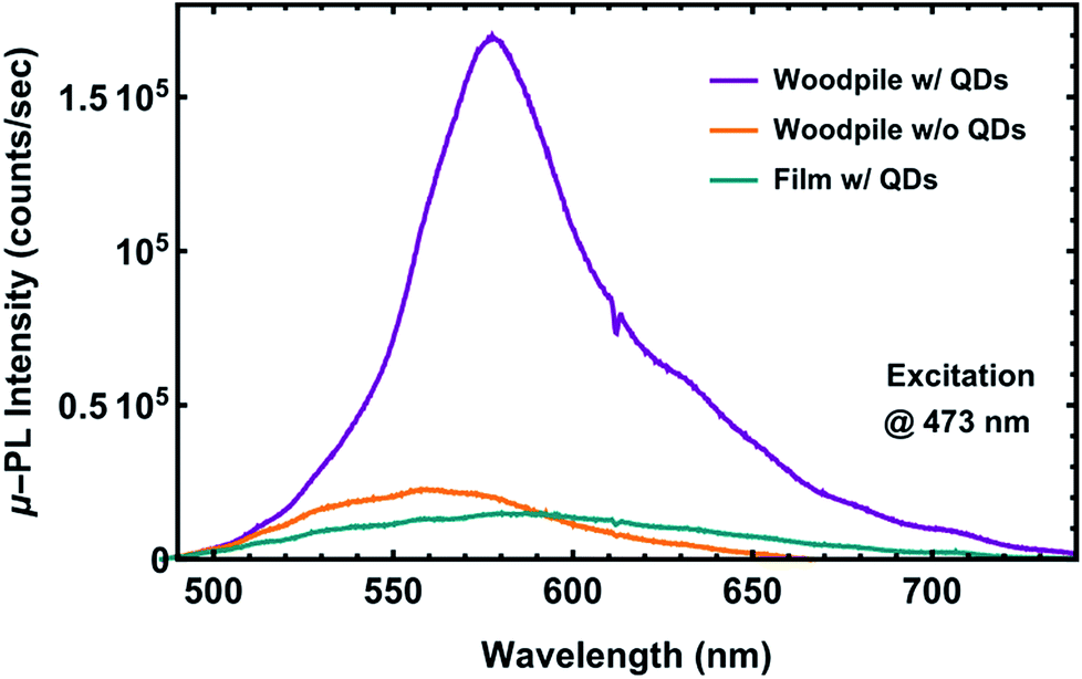 | ||
| Fig. 7 Micro-photoluminescence (μ-PL) spectra from a woodpile photonic structure: before (orange) and after (purple) in situ synthesis of CdS quantum dots (QDs). Also, μ-PL spectra from a thin polymer film (green) functionalized with CdS QDs is shown. | ||
Time-resolved pump-probe measurements
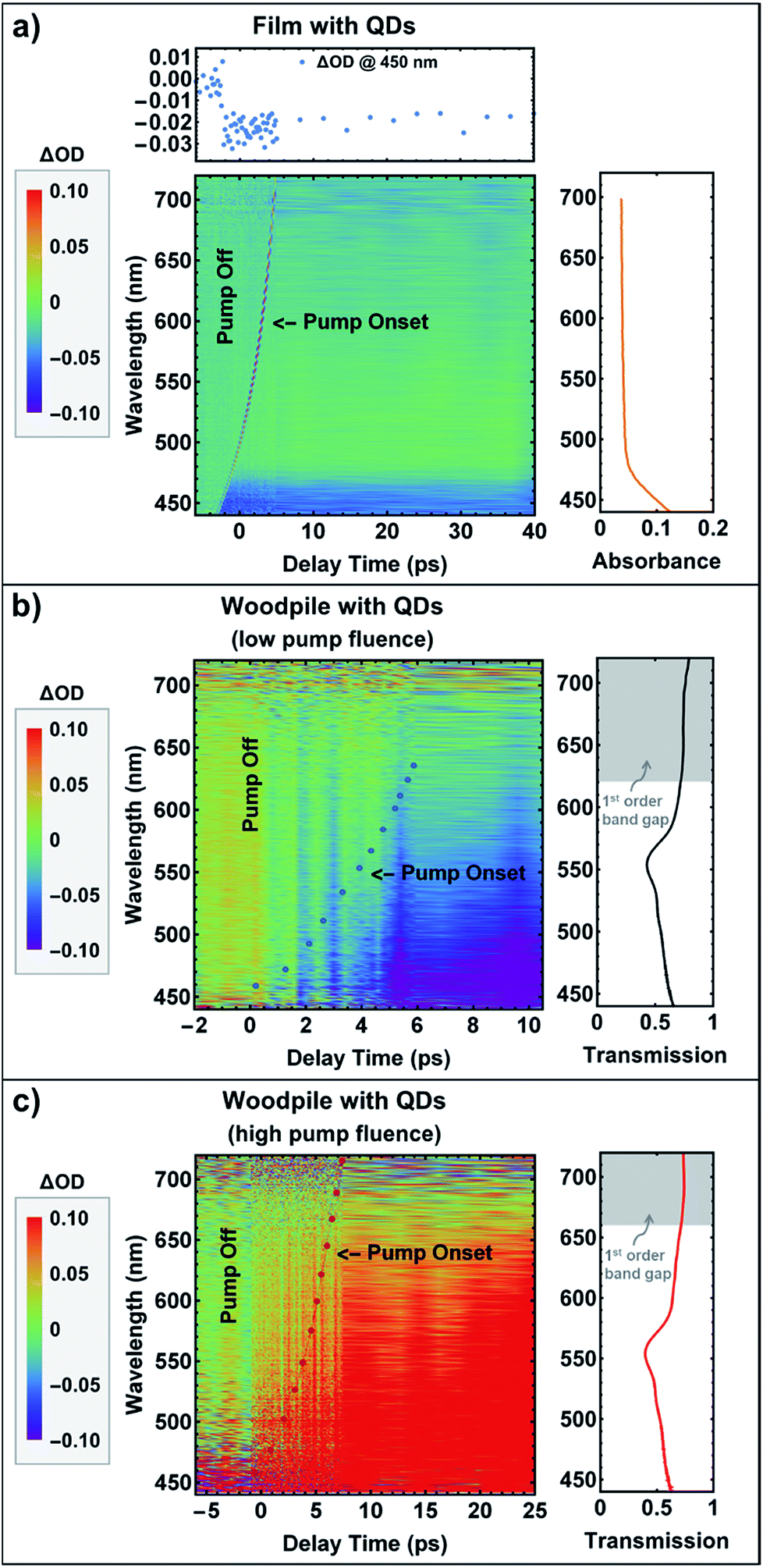
The dynamic tuning of photonic properties of the fabricated 3D woodpile photonic structures functionalized with CdS QDs was investigated through a time-resolved differential pump-probe technique.41 With strong pumping, a femtosecond shifting of the photonic-band-gap is expected as a result of the changes induced in the refractive index of the backbone material in the photonic matrix due to the Kerr nonlinearity. Optimal homogeneous switching is expected especially near the first order band gap and for pump wavelengths for which a Kerr nonlinearity can be induced.42 Therefore, for all measurements presented here, the sample is homogeneously excited by a pump beam centered at 795 nm, while it is probed by measuring transmittance in the wavelength range from 440 nm to 720 nm as a function of pump-probe delay time. Differential pump-probe measurements were achieved by splitting of the probe beam into two parts that were used as Signal and Reference. The detailed experimental setup and measuring scheme is provided in the Experimental section.Initially, prior to recording the dynamic tuning of the photonic-band-gap properties, a complementary tracking of the CdS exciton dynamics was provided by a transient absorption experiment carried out for the case of a QD containing polymer film. The time-resolved differential pump-probe measurements obtained are shown in the main panel of Fig. 8(a), where a time-resolved spectral representation of the changes in the optical density (ΔOD) (z-axis, color-axis) as a function of wavelength (y-axis) and the pump-probe delay time (x-axis) is displayed (see Experimental section for details). Regions appearing red show a positive change in the optical density (OD), while those appearing blue represent negative change in the OD as shown on the color-scale on the left-hand side. The zero pump-probe delay is also recorded as a cross-correlation parabolic-like trace between the scattered pump light from the sample and a delayed white light pulse. Note that the time-zero of the experiment is not unique and varies with the probe wavelength. This is due to the chromatic dispersion that the broadband white light supercontinuum probe beam has attained since its generation. As one can observe, a spectral region where ΔOD < 0 (blue region) is recorded at wavelengths shorter than 475 nm, just after the arrival of the excitation pulse, (incident pump fluence at ∼17.5 mJ cm−2) hinting at a femtosecond rise-time, which correlates to the exciton binding energy of CdS. Given that the pump operates at 795 nm, this is clear evidence of a nonlinear process, which is in fact two-photon absorption and is in accordance with the linear absorption spectrum obtained from UV-Vis spectroscopy (right panel, also shown in Fig. 2).
 | ||
| Fig. 8 Pump-probe measurements on a quantum dot (QD) doped polymer film (a) and a woodpile structure at low (b) and high (c) incident pump fluence: (a) Main panel: Spectrogram of the changes in optical density (ΔOD) of transient absorption as a function of wavelength and pump-probe delay time. Left panel: Color-scale representing the range of ΔOD values. Upper panel: Temporal cross-section of ΔOD(Δt) at the wavelength of 450 nm. Right panel: UV-Vis absorption spectrum of the QD doped polymer film (also shown in Fig. 2). (b) and (c): a QD doped woodpile structure with 550 nm (b) and 600 nm (c) inlayer periodicity. The red/blue dots in the main panel are a guide to the eye indicating the cross-correlation trace of pump-probe delay. Right panel: Transmission spectrum of the QD doped woodpile structure (also shown in Fig. 5(b)). The gray region represents the position of the fundamental photonic-band-gap. Incident pump fluence: (a) ∼17.5 mJ cm−2, (b) ∼1.25 mJ cm−2, (c) ∼11 mJ cm−2. | ||
Note that the ΔOD is defined as ΔOD = log[IRef/ISig], where ISig is the power transmitted from the sample (Signal) and IRef is the power transmitted from the Reference. In the absence of pump, IRef/ISig is equal to 1 and, therefore, ΔOD = 0. Hence, ΔOD tracks changes in the transmittance from the sample due to the presence of the pump; absence of pump or no change due to the presence of the pump yields ΔOD = 0 marked as green areas on the plot, while increased transmission corresponds to ΔOD < 0 marked as blue regions, and reduced transmission as ΔOD > 0 appearing as red regions. In the case of a QD containing film, before the pump is applied, the probe beam is subject to absorption according to the spectra shown in Fig. 2 (Film w/QDs). Once the pump is present, the population is excited as the pump is absorbed by the film and, therefore, when the probe arrives thereafter, less population is available in the ground state to absorb the probe power leading to a reduced absorption and, hence, an increased transmittance from the film (compared to the absence of the pump). This is manifested as ΔOD < 0 i.e., the blue region shown in Fig. 8(a). Of course, after excitation, the population starts relaxing and as the pump-probe delay is increased, this is experienced by the probe as increased absorption (more population is available in the ground state to absorb the probe power). Eventually, for very long delays the population return to its ground state and is all available again to be absorbed entirely by the probe (not shown for the time window chosen here).
In addition, a temporal cross-section of ΔOD(Δt) at the wavelength of 450 nm is also depicted in Fig. 8(a), upper panel, where the observed dynamics reflect the energy relaxation and recombination of the photo-excited carriers. The results obtained are typical for II–VI QDs embedded in a glass/polymer matrix usually consisting of fast initial decay components with characteristic time constants from tens of femtoseconds to several picoseconds followed by a slower nanosecond decay.43–45 Furthermore, in order to eliminate any effect arising from the pure polymer film, a similar experiment was carried out for a non-doped sample containing only the Cd2+ polymer composite, where no pump-induced change was recorded in the OD as expected (ESI, Fig. S3†).
Time-resolved differential pump-probe measurements were carried out for the case of a woodpile structure functionalized with CdS QDs, which are shown in the main panel of Fig. 8(b). On the right panel, the linear transmission spectrum of the respective woodpile photonic structure with 550 nm inlayer periodicity is displayed (also shown in Fig. 5(b)) in order to facilitate the comparison of the dynamics. The location of the fundamental photonic stop-band is marked as a grey region. On the left panel, the color-scale representing the range of the recorded ΔOD values is depicted. As one can observe, upon low pump excitation (∼1.25 mJ cm−2), a spectral region where ΔOD < 0 is recorded on the right-hand side of the zero delay line (marked as a blue dotted line) for a wide wavelength range below the short-wavelength band gap edge for a long time period of several ps (>10 ps). In particular, negative values of the OD are recorded upon excitation that build up for positive time delays indicating that IRef/ISig < 1 i.e., the transmittance from the woodpile structure increases. Following the same reasoning as for the case of a QD containing film, this pump-induced response recorded upon low pump excitation corresponds to nonlinear absorption. In fact, the nonlinear absorption recorded for the functionalized woodpile structure is observed for longer wavelengths than for the case of a QD containing film (extending approximately up to 500 nm) due to the larger QDs formed on the 3D polymer photonic matrix compared to the QD containing polymer film. Moreover, time-resolved differential pump-probe measurements at high excitation levels (∼18.1 mJ cm−2) were carried out for a non-doped woodpile photonic crystal in order to confirm that the pump-induced changes observed for a doped sample are not due to the polymer matrix. The results obtained for a pure polymer woodpile structure with 600 nm inlayer periodicity are shown in Fig. S5 (ESI†), where no pump-induced change of the OD was recorded.
The outcome of the pump-probe experiment at high pump intensities (∼11 mJ cm−2) for a woodpile structure with 600 nm inlayer periodicity functionalized with CdS QDs is displayed in the main panel of Fig. 8(c). As seen, an intense pump-induced change in the differential signal dynamics is recorded on the right-hand side of the zero delay line (marked as a red dotted line) for a wide wavelength range below the short-wavelength band gap edge for a long time period of several ps (>25 ps). In particular, positive values of the OD are recorded upon excitation that build up for positive time delays indicating that IRef/ISig > 1 i.e., the transmittance from the woodpile structure reduces. This is a surprising result because a pump-induced absorption could only increase the transmittance, as explained earlier for the case of the QD containing film; this is also what occurs with low pump power in the functionalized woodpile photonic crystal. Additionally, a possible pump-induced emission of the QDs (either in the film or in the woodpile), would again manifest as increased probe transmittance due to the additional emitted photons from the gain material (QDs). Clearly, in the functionalized woodpile structure, while for low pump power the transmittance increases, for high pump power the transmittance reduces implying fundamental changes in the system's response due to the pump. These changes could possibly originate from a pump-induced shift of the photonic-band-gap, or even from damage of the woodpile photonic crystal due to high pump excitation, which could lead to lower probe intensity being recorded due to scattering. However, Fourier transformed infrared (FTIR) linear transmission measurements performed on the same woodpile system after the excitation revealed that the woodpile structure remained intact (Fig. S4, ESI†). Note that the inlayer periodicity of the woodpile structures examined in Fig. 8(b) and (c) varies from 550 nm to 600 nm. Due to this change, the location of the fundamental photonic stop band shifts from 710 nm to 760 nm, accordingly, and, therefore, the magnitude of ΔOD is not directly comparable. However, qualitatively, the response of the two systems is comparable, both because of the proximity of the two band gaps (50 nm apart) and, also, because the band gaps, as well as the pump wavelength (795 nm), are located far from the QD absorption (<500 nm). Hence, based on the sign of ΔOD, which is related to qualitatively different phenomena, we can draw the above conclusions for our systems, despite the different periodicity.
According to photonic-band-structure calculations for photonic-band-gap materials possessing Kerr nonlinearity, a positive change in refractive index would lead to a “blue” shift of both photonic band edges along with a significant widening of the photonic-band-gap.46–48 In our case, a pump-induced response of the QD containing woodpile structures is observed on a sub-picosecond time scale mainly recorded for a wide wavelength range below the short-wavelength band gap edge. In addition, the recorded signal rises further at positive time delays (>10 ps) instead of rapidly decaying as the photonic feature would relax back to its original wavelength, also reported previously in analogous experiments involving 3D nonlinear photonic crystals.49–51 However, in most of the previous works, semiconductor materials such as gallium arsenide or silicon were utilized, where large-refractive index-contrast photonic crystals could be obtained. Additionally, in order to achieve high intensity contrast between “on” and “off” states of the optical switching, a monochromatic probe beam with a central wavelength located at the short-wavelength band gap edge was employed, instead of a white light super-continuum probe as in the present work.
Although, in our case, a clear ultrafast dynamic response is recorded from the woodpile photonic structure functionalized with CdS QDs, that indicates a photonic-band-gap shift, further experiments need to be carried out in order to identify the competing ultrafast all-optical switching mechanisms that take place between the 3D polymer photonic matrix and the functionalized QDs5 for a comprehensive understanding of the underlying effects in order to reach more solid conclusions. Such a complementary study of the mechanisms is planned to be carried out in a future work.
Conclusions
Visible light active 3D woodpile photonic devices are successfully fabricated containing an organic–inorganic silicon–zirconium composite and CdS QDs. The structures are realized by the combination of diffusion-assisted DLW by two-photon absorption and the in situ synthesis of CdS QDs. The novel active 3D printable hybrid composite material exhibits a high nonlinear refractive index value measured by means of the Z-scan method, whereas the fabricated woodpile structures show clear photonic stop bands in the visible wavelength region. By means of time-resolved pump-probe spectroscopy, indication of a photonic-band-gap shift is demonstrated. It is expected that the nanocomposite material presented herein can find applications in active micro/nanodevices, such as ultrafast switching and modulation applications.Experimental
Direct laser writing
3D photonic architectures are fabricated employing Direct Laser Writing by two photon absorption using a home-built experimental setup. The laser source employed is a Ti:sapphire femtosecond oscillator operating at 800 nm with a pulse length of <20 fs and a repetition rate of 75 MHz. A 100× microscope objective lens (Zeiss, Plan Apochromat, N.A. = 1.4) was used to focus the laser beam into the volume of the photosensitive material. The writing speed employed was 20 μm s−1 and the peak intensity at the center of the focal point was ∼0.35 TW cm−2. The complete experimental setup and writing procedure has been described elsewhere.29 After the completion of the component building process, the samples were developed for 30 min in ethanol and were further rinsed with 2-propanol. In sequence, the samples were immersed for 6 hours in a sodium sulfide non-hydrate (Na2S·9H2O ASC reagent Sigma Aldrich) aqueous solution 0.07 M for the in situ synthesis of CdS QDs. Finally, they were rinsed several times with nano pure water and left to dry at room temperature.In the present work, for the fabrication of 3D photonic devices by DLW, the woodpile geometry was chosen.38 It consists of layers of one dimensional rods with a stacking sequence that repeats itself every four layers (accounting for one unit cell). The distance between four adjacent layers is c and within each layer, the axes of the rods are parallel to each other with a distance α between them (see Fig. 6(c)). The adjacent layers are rotated by 90°. Between every other layer, the rods are shifted relative to each other by α/2.
Material synthesis
All chemicals were obtained from Sigma-Aldrich and used without further purification. The material employed for the preparation of the woodpile photonic structures is an organic–inorganic zirconium–silicon hybrid composite27 doped with the quencher 2-(dimethylamino)ethyl methacrylate (DMAEMA).16,32 It consists of methacryloxy-propyl trimethoxysilane (MAPTMS), zirconium propoxide (ZPO, 70% in propanol), methacrylic acid (MAA), and DMAEMA. In the present work, Cd(MA)2 were added in the composite material in order to serve as precursors for CdS QDs. MAPTMS, MAA, DMAEMA and Cd(MA)2 were used as the organic photopolymerizable monomers, while ZPO and the alkoxysilane groups of MAPTMS were used to form the inorganic network. The organic–inorganic hybrid material was synthesized by mixing the above chemicals in the following molar ratios: MAPTMS![[thin space (1/6-em)]](https://www.rsc.org/images/entities/char_2009.gif) :ZPO = 8:2, ZPO:MAA = 1:1, (MAPTMS + ZPO):DMAEMA = 7:3, and Cd(MA)2:ZPO = 1:1. Michler's ketone (4,4-bis(diethylamino)benzophenone) was used as a photoinitiator and added at 1% w/w concentration to the final solution of MAPTMS and DMAEMA composite.
:ZPO = 8:2, ZPO:MAA = 1:1, (MAPTMS + ZPO):DMAEMA = 7:3, and Cd(MA)2:ZPO = 1:1. Michler's ketone (4,4-bis(diethylamino)benzophenone) was used as a photoinitiator and added at 1% w/w concentration to the final solution of MAPTMS and DMAEMA composite.
Initially, Cd(MA)2 was prepared by mixing cadmium oxide (CdO) powder with MAA at a 1 over 2 molar ratio. More specifically, CdO was added in portions in a flask containing MAA and 1.5 ml of ethanol at room temperature. In sequence, the mixture was left stirring for 24 hours until the desired product was obtained. Next, MAPTMS was hydrolyzed with the addition of HCl (0.1 M) and the mixture was stirred for 15 min. In a separate flask, ZPO was chelated by adding MAA in the presence of 145 μl of 1-propanol (1-PrOH) and left stirring for 20 min. Then, the hydrolyzed MAPTMS was added drop-wise to the ZPO sol following another 20 min of stirring. In sequence, Cd(MA)2 was added to the flask and left stirring for 30 min. Finally, the composite material was filtered using 0.22 μm pore size filters. The samples were prepared by drop casting onto 100 μm thick glass substrates and the resultant films were dried in air for several days before photo-polymerization.
Time-resolved pump-probe spectroscopy
Pump-probe time-resolved transmission measurements are recorded by employing an amplified femtosecond Ti-sapphire laser operating at 795 nm, with a pump pulse duration of ∼30 fs, a pulse repetition rate of 1 kHz and pulse energy amplified to ∼1 mJ per pulse. At the exit of the amplifier, the laser beam splits into two arms; one arm serves as a weak probe beam, and the other one as a pump beam. The probe beam is tightly focused into a quartz cuvette filled with distilled water in order to generate a white light supercontinuum source via optical rectification and plasma52,53 providing a broad spectral wavelength range from 440 nm to 720 nm. The supercontinuum pulses, after propagating through a telescope in order to maintain beam collimation, are guided to a delay line which enables control of the length of the probe arm. This change of optical path sets the relative time delay (Δt) between pump and probe pulses. The white light probe beam further splits into two arms by a beam splitter; one arm serves as the probe Signal and the other one as the probe Reference. The probe Signal is focused by a lens into a 25 μm spot at the sample surface, whereas the latter is vertically displaced and focused by a similar lens to an unperturbed area on the sample. The sample holder is mounted on top of a rotation stage, so that the sample can be rotated by an angle with respect to the optical axis, while the whole combination is mounted on top of a three-dimensional translational stage in order to align the sample relative to the focus. The light is coupled out and collected by a lens at the entrance of the detection system, which consists of a monochromator with a CCD camera mounted at its exit. The sample plane is also inspected with a camera system in order to ensure that the light collected has passed through the desired woodpile structure sitting on the sample. Incident fluence is calculated by recording both beam profiles at the focal plane of the probe beam by use of a CCD camera. Note that the size of the pump beam focus is much larger (∼180 μm) than that of the probe beam, thus achieving homogeneous excitation of the probed sample area.The optical density (OD) of the transient absorption is extracted from measurements of the transient spectra calculated as the ratio of the probe pulse intensity being transmitted through an unperturbed sample area (probe Reference, IRef(ν)) and that collected from a perturbed sample area (probe Signal, ISig(ν)) for times prior to and after excitation by the pump as defined in ref. 41, page 231.41,54
Z-scan measurements
The nonlinear absorption of the quantum dot containing composite material was investigated using the Z-scan technique. The laser source employed is a regenerative Ti:sapphire amplifier (Tsunami, SpectraPhysics), operating at 800 nm, with <250 fs pulse width and 1 kHz repetition rate. The laser beam was focused with a 10 cm lens onto a thin polymeric film of the quantum dot containing material and the sample was moved with motorized stages along the beam propagation axis. The complete experimental set-up and measuring scheme has been described elsewhere.55Theoretical calculations
The theoretical band structure of the infinite woodpile photonic crystal with an inlayer periodicity a = 600 nm has been calculated with the freely available MIT photonic bands (MPB) software.56 The refractive index of the dielectric rods was set to n = 1.52. The cross-section of the rods was assumed for simplicity to be rectangular having the same area (rod thickness (d) × rod height (h) = 80 nm × 240 nm) as the actual elliptical rods (120 nm × 360 nm) and preserving the 1/3 = thickness/height ratio (due to the objective lens) to ensure that their shape does not affect the band gap properties. In order to simulate the transmission and reflection from the finite experimental sample of 10 unit cells, a custom Finite Difference Time Domain (FDTD) code was employed using the same geometrical parameters as before, while assuming that the structure is infinite in the inlayer plane. The discrete time and space steps were set to δt = 15 × 10−18 s and δx = 10 × 10−9 m, respectively. In order to take into account the experimental scattering losses, artificial loss (conductivity) was introduced into the dielectric rods equal to σ = 3 × 10³ S, corresponding to an imaginary part of ∼0.1 for the rod permittivity.Optical measurements
FTIR transmittance/reflectance spectra shown in Fig. S4 (ESI†) were measured with a Vertex 80 spectrometer coupled to a Hyperion 2000 IR microscope (Bruker Optics) which was equipped with Cassegrain objectives (15×, 36×) and a liquid nitrogen cooled mercury cadmium telluride detector. While transmittance/reflectance measurements shown in Fig. 5 were acquired employing a white light transmission/reflection spectroscopy system similar to the one described in ref. 57.57Micro-photoluminescence measurements
Micro-photoluminescence (μ-PL) spectra were collected in a backscattering setup using an excitation source of 473 nm continuous wave laser through a 40× objective with a numerical aperture of 0.65 forming a 1 μm spot diameter. The excitation power for all measurements was set to 6 μW. The detailed experimental setup is described in ref. 58.58Conflicts of interest
There are no conflicts to declare.Acknowledgements
The research leading to these results has received funding from LASERLAB-EUROPE (grant agreement no. 654148, European Union's Horizon 2020 research and innovation programme). It has also being supported by the European Union's Horizon 2020 research and innovation programme under the Marie Skłodowska-Curie grant agreement no. 655249. Ioanna Sakellari thanks Stavros Niarchos Foundation for financial support (ARCHERS project). The authors would also like to thank Florian Sterl and Dr Nikolai Strohfeldt for assistance with optical spectroscopy measurements, as well as, Dr Ioannis Paradisanos and Ioanna Demeridou for performing the μ-PL measurements acquired.Notes and references
- P. Prabhakaran, W. J. Kim, K.-S. Lee and P. N. Prasad, Opt. Mater. Express, 2012, 2, 578 CrossRef CAS.
- J. C. Norman, D. Jung, Y. Wan and J. E. Bowers, APL Photonics, 2018, 3, 030901 CrossRef.
- T. Rath and G. Trimmel, Hybrid Mater., 2014, 1, 15 Search PubMed.
- H. Kim, S. Beack, S. Han, M. Shin, T. Lee, Y. Park, K. S. Kim, A. K. Yetisen, S. H. Yun, W. Kwon and S. K. Hahn, Adv. Mater., 2018, 30, 1–33 Search PubMed.
- P. Lodahl, S. Mahmoodian and S. Stobbe, Rev. Mod. Phys., 2015, 87, 347–400 CrossRef CAS.
- L. Banyai, Y. Z. Hu, M. Lindberg and S. W. Koch, Phys. Rev. B: Condens. Matter Mater. Phys., 1988, 38, 8142–8153 CrossRef.
- E. Yablonovitch and T. J. Gmitter, J. Opt. Soc. Am. A, 1990, 7, 1792–1800 CrossRef CAS.
- K. M. Ho, C. T. Chan and C. M. Soukoulis, Phys. Rev. Lett., 1990, 65, 3152–3155 CrossRef CAS.
- S. Bin Hasan, A. P. Mosk, W. L. Vos and A. Lagendijk, Phys. Rev. Lett., 2018, 120, 237402 CrossRef PubMed.
- C. López, J. Opt. A: Pure Appl. Opt., 2006, 8, R1–R14 CrossRef.
- S. C. Padmanabhan, K. Linehan, S. O'Brien, S. Kassim, H. Doyle, I. M. Povey, M. Schmidt and M. E. Pemble, J. Mater. Chem. C, 2014, 2, 1675–1682 RSC.
- P. Lodahl, A. F. Van Driel, I. S. Nikolaev, A. Irman, K. Overgaag, D. Vanmaekelbergh and W. L. Vos, Nature, 2004, 430, 654–657 CrossRef CAS.
- J. Li, B. Jia, G. Zhou, C. Bullen, J. Serbin and M. Gu, Adv. Mater., 2007, 19, 3276–3280 CrossRef CAS.
- M. Qi, E. Lidorikis, P. T. Rakich, S. G. Johnson, J. D. Joannopoulos, E. P. Ippen and H. I. Smith, Nature, 2004, 429, 538–542 CrossRef CAS.
- J. Stampfl, R. Liska and A. Ovsianikov, Multiphoton Lithography, Wiley-VCH, Weinheim, 2016 Search PubMed.
- I. Sakellari, E. Kabouraki, D. Gray, V. Purlys, C. Fotakis, A. Pikulin, N. Bityurin, M. Vamvakaki and M. Farsari, ACS Nano, 2012, 6, 2302–2311 CrossRef CAS.
- J. Fischer, G. von Freymann and M. Wegener, Adv. Mater., 2010, 22, 3578–3582 CrossRef CAS.
- J. Fischer and M. Wegener, Laser Photonics Rev., 2013, 7, 22–44 CrossRef CAS.
- B. Jia, D. Buso, J. Van Embden, J. Li and M. Gu, Adv. Mater., 2010, 22, 2463–2467 CrossRef CAS.
- R. Krini, C. W. Ha, P. Prabhakaran, H. El Mard, D.-Y. Yang, R. Zentel and K.-S. Lee, Macromol. Rapid Commun., 2015, 36, 1108–1114 CrossRef CAS.
- D. Buso, E. Nicoletti, J. Li and M. Gu, Opt. Express, 2010, 18, 1033–1040 CrossRef CAS.
- Z. Bin Sun, X. Z. Dong, W. Q. Chen, S. Nakanishi, X. M. Duan and S. Kawata, Adv. Mater., 2008, 20, 914–919 CrossRef.
- Z. B. Sun, X. Z. Dong, S. Nakanishi, W. Q. Chen, X. M. Duan and S. Kawata, Appl. Phys. A: Mater. Sci. Process., 2007, 86, 427–431 CrossRef CAS.
- B.-B. Xu, Y.-L. Zhang, R. Zhang, L. Wang, X.-Z. Xiao, H. Xia, Q.-D. Chen and H.-B. Sun, J. Mater. Chem. C, 2013, 1, 4699 RSC.
- M. J. Ventura, C. Bullen and M. Gu, Opt. Express, 2007, 15, 1817–1822 CrossRef CAS.
- K. K. Jang, P. Prabhakaran, D. Chandran, J.-J. Park and K.-S. Lee, Opt. Mater. Express, 2012, 2, 519 CrossRef CAS.
- A. Ovsianikov, J. Viertl, B. Chichkov, M. Oubaha, B. MacCraith, I. Sakellari, A. Giakoumaki, D. Gray, M. Vamvakaki, M. Farsari and C. Fotakis, ACS Nano, 2008, 2, 2257–2262 CrossRef CAS.
- J. Zha and H. Roggendorf, Adv. Mater., 1991, 3, 522 Search PubMed.
- I. Sakellari, A. Gaidukeviciute, A. Giakoumaki, D. Gray, C. Fotakis, M. Farsari, M. Vamvakaki, C. Reinhardt, A. Ovsianikov and B. N. Chichkov, Appl. Phys. A: Mater. Sci. Process., 2010, 100, 359–364 CrossRef CAS.
- A. Pikulin, N. Bityurin and V. I. Sokolov, AIP Adv., 2015, 5, 127215 CrossRef.
- G. Bickauskaite, M. Manousidaki, K. Terzaki, E. Kambouraki, I. Sakellari, N. Vasilantonakis, D. Gray, C. M. Soukoulis, C. Fotakis, M. Vamvakaki, M. Kafesaki, M. Farsari, A. Pikulin and N. Bityurin, Adv. OptoElectron., 2012, 2012, 1–6 CrossRef.
- I. Sakellari, X. Yin, M. L. Nesterov, K. Terzaki, A. Xomalis and M. Farsari, Adv. Opt. Mater., 2017, 5, 1700200 CrossRef.
- M. Moffitt, L. McMahon, V. Pessel and A. Eisenberg, Chem. Mater., 1995, 7, 1185–1192 CrossRef CAS.
- Z. Bin Sun, X. Z. Dong, W. Q. Chen, S. Shoji, X. M. Duan and S. Kawata, Nanotechnology, 2008, 19, 035611 CrossRef.
- M. Sheik-Bahae, A. A. Said, T. H. Wei, D. J. Hagan and E. W. Van Stryland, IEEE J. Quantum Electron., 1990, 26, 760–769 CrossRef CAS.
- V. Q. Lam, S. Turrell, A. Martucci, M. Bouazaoui and B. Capoen, J. Non-Cryst. Solids, 2006, 352, 3315–3319 CrossRef CAS.
- Y. Lin, J. Zhang, E. Kumacheva and E. H. Sargent, J. Mater. Sci., 2004, 39, 993–996 CrossRef CAS.
- K. M. Ho, C. T. Chan, C. M. Soukoulis, R. Biswas and M. Sigalas, Solid State Commun., 1994, 89, 413–416 CrossRef CAS.
- M. Deubel, G. Von Freymann, M. Wegener, S. Pereira, K. Busch and C. M. Soukoulis, Nat. Mater., 2004, 3, 444–447 CrossRef CAS PubMed.
- I. Staude, M. Thiel, S. Essig, C. Wolff, K. Busch, G. von Freymann and M. Wegener, Opt. Lett., 2010, 35, 1094–1096 CrossRef CAS PubMed.
- C. Rullière, Femtosecond Laser Pulses, Springer, New York, 2005 Search PubMed.
- P. M. Johnson, A. F. Koenderink and W. L. Vos, Phys. Rev. B: Condens. Matter Mater. Phys., 2002, 66, 1–4 Search PubMed.
- P. Horodyská, P. Němec, D. Sprinzl, P. Malý, V. N. Gladilin and J. T. Devreese, Phys. Rev. B: Condens. Matter Mater. Phys., 2010, 81, 045301 CrossRef.
- M. Shui, X. Jin, Z. Li, J. Yang, G. Shi, Z. Nie, X. Wu, Y. Wang, K. Yang, X. Zhang and Y. Song, J. Mod. Opt., 2011, 58, 973–977 CrossRef CAS.
- V. I. Klimov, D. W. McBranch, C. A. Leatherdale and M. G. Bawendi, Phys. Rev. B: Condens. Matter Mater. Phys., 1999, 60, 13740–13749 CrossRef CAS.
- P. Tran, Phys. Rev. B: Condens. Matter Mater. Phys., 1995, 52, 10673–10676 CrossRef CAS.
- V. Lousse and J. P. Vigneron, Phys. Rev. E: Stat., Nonlinear, Soft Matter Phys., 2001, 63, 027602 CrossRef CAS.
- A. Huttunen and P. Törmä, J. Appl. Phys., 2002, 91, 3988–3991 CrossRef CAS.
- T. G. Euser, A. J. Molenaar, J. G. Fleming, B. Gralak, A. Polman and W. L. Vos, Phys. Rev. B: Condens. Matter Mater. Phys., 2008, 77, 115214 CrossRef.
- Y. Liu, F. Qin, Z.-Y. Wei, Q.-B. Meng, D.-Z. Zhang and Z.-Y. Li, Appl. Phys. Lett., 2009, 95, 131116 CrossRef.
- P. J. Harding, T. G. Euser and W. L. Vos, J. Opt. Soc. Am. B, 2009, 26, 610 CrossRef CAS.
- R. R. Alfano and S. L. Shapiro, Phys. Rev. Lett., 1970, 24, 592–594 CrossRef CAS.
- R. R. Alfano, The supercontinuum laser source: fundamentals with updated references, Springer, New York, 2006 Search PubMed.
- A. Maciejewski, R. Naskrecki, M. Lorenc, M. Ziolek, J. Karolczak, J. Kubicki, M. Matysiak and M. Szymanski, J. Mol. Struct., 2000, 555, 1–13 CrossRef CAS.
- E. Kabouraki, A. N. Giakoumaki, P. Danilevicius, D. Gray, M. Vamvakaki and M. Farsari, Nano Lett., 2013, 13, 3831–3835 CrossRef CAS.
- S. Johnson and J. Joannopoulos, Opt. Express, 2001, 8, 173 CrossRef CAS.
- F. Sterl, N. Strohfeldt, R. Walter, R. Griessen, A. Tittl and H. Giessen, Nano Lett., 2015, 15, 7949–7955 CrossRef CAS.
- I. Paradisanos, S. Germanis, N. T. Pelekanos, C. Fotakis, E. Kymakis, G. Kioseoglou and E. Stratakis, Appl. Phys. Lett., 2017, 110, 193102 CrossRef.
Footnote |
| † Electronic supplementary information (ESI) available: EDS measurements on a woodpile photonic crystal before and after in situ synthesis of CdS QDs. Also, pump-probe measurements on a pure polymer film, as well as, on a woodpile structure with 600 nm inlayer periodicity prior to in situ synthesis of CdS QDs. In addition, transmission measurements for a woodpile structure with 600 nm inlayer periodicity functionalized with CdS QDs before and after high pump excitation. And, finally, an XRD pattern of a polymer film functionalized with CdS QDs. See DOI: 10.1039/c9na00357f |
| This journal is © The Royal Society of Chemistry 2019 |