
 Open Access Article
 This Open Access Article is licensed under a Creative Commons Attribution-Non Commercial 3.0 Unported Licence
Fluorescence enhanced lab-on-a-chip patterned using a hybrid technique of femtosecond laser direct writing and anodized aluminum oxide porous nanostructuring†
Zhi
Yu
ac,
Yuhao
Lei
a,
Weili
Yu
ac,
Jinluo
Cheng
ac,
Jun
Xing
ac,
Xin
Zheng
ac,
Zhibing
Zhan
b,
Bin
Wang
ac and
Chunlei
Guo
 *abc
*abc
aThe Guo China-US Photonics Laboratory, Changchun Institute of Optics, Fine Mechanics and Physics, Chinese Academy of Sciences, Changchun, China 130033
bThe Institute of Optics, University of Rochester, Rochester, NY 14627, USA. E-mail: guo@optics.rochester.edu
cState Key Laboratory for Applied Optics, Changchun Institute of Optics, Fine Mechanics and Physics, Chinese Academy of Sciences, Changchun, China 130033
First published on 15th July 2019
Abstract
In this paper, we demonstrate a simple yet effective hybrid method to fabricate lab-on-a-chip devices on aluminum (Al) foil. Instead of using conventional photoresists and lithography methods, an array of square units is first produced by femtosecond laser direct writing, followed by generating highly ordered anodized aluminum oxide (AAO) nanoporous structures within each unit. The AAO treated area becomes hydrophilic. Next, we functionalize the surrounding area outside the square units to superhydrophobic by electrochemical deposition and further chemical modification. This hydrophilic and hydrophobic pattern allows us to confine the liquid samples to be detected within the hydrophilic AAO detection area. We use rhodamine 6G (R6G) as a probe, and obtain a fluorescence intensity enhancement from R6G by 70 times over a flat surface. This leads to the detection sensitivity of R6G molecules to a concentration as low as 10−17 mol L−1. By mixing R6G with RhB molecules, the fluorescence emission bands shift significantly due to the addition of RhB molecules, showing a significantly improved spectral resolution compared to traditional fluorescence spectrometers for liquid samples. This phenomenon can be attributed to the energy transfer between R6G and RhB under laser excitation, which was enhanced by the AAO nanostructures. The array-based LOC device demonstrated in this paper is simple and convenient to fabricate, has low sample consumption and dramatically enhances the fluorescence yield with improved spectral resolution.
Introduction
The lab-on-a-chip (LOC) system has attracted tremendous attention in various research fields, such as biology, chemistry, medical science etc.1–3 A LOC system, composed of array-based, continuous microfluidics, encoded bead and digital microfluidics platforms, can detect, integrate, separate, and process biological and chemical samples in order to achieve more complex analyses.4–7 Each LOC device can be assembled with other types of platforms for more efficient sample handling and analysis. A LOC usually includes many repetitive structure units for high-throughput analysis with a small volume of samples, and the advantages of these miniaturized analytical systems include accuracy improvement, multiplexing, lower sample and reagent consumption, disposability and decreased analysis times.8–10 Array-based LOC detection systems are mostly functionalized by further integration procedures, and exhibit special physical and chemical properties. Such integrated devices can realize the detection and analysis in some specific fields with much better sensitivity and resolutions. In the past, larger scale structures were typically prepared with lithography methods, which require masks and multi-step processes.11–13 It can be rather complicated when frequent patch size adjustments are needed, thus leading to several disadvantages, such as nonreusability and adsorption of organic compounds.14 On the other hand, femtosecond laser direct writing is a clean method to produce a high-quality cut with arbitrary shape and dimension.15During the past few decades, we have witnessed tremendous developments of ultrafast lasers, which have become more user-friendly and cost effective.16 Ultrafast femtosecond lasers have occupied a very important position in materials machining. Although nanosecond lasers were commonly used in machining, the thermal effects from machining with relatively long ns-lasers can lead to a larger heat-affected zone, lower machining quality, and greater collateral damage such as stresses, cracks, and molten layer recast and slag.17 By contrast, femtosecond lasers provide an ideal machining quality with high spatial resolution and minimal thermal damage. Due to the ultrafast pulse length, femtosecond lasers can deliver energy in a controllable manner.18 The heat diffusion around the machined area is minimal and the heat-affected zone is very small with a small amount of molten material and a low level of thermal defects left behind.19 They show much better advantages than traditional laser processing techniques, specifically, energy deposition in a time scale shorter than that for electron–phonon coupling processes in any material due to the ultrashort pulse width which can suppress the formation of the heat-affected zone allowing laser processing with high precision and resolution.20 The unique advantage of femtosecond laser processing over conventional methods resides in the capability of sculpting complex three dimensional shapes at micro- and nanoscales in transparent materials, both for inorganic and organic materials.21,22 One can precisely set the interaction region in a localized area of either surfaces or in volume by employing focused ultrashort pulses with extremely high peak intensities for spot machining.15,23,24 As a consequence, femtosecond laser technologies have been increasingly developed and extensively applied to the fabrication of LOC devices and integration of multifunctional components or specific functional materials into localized positions of LOC devices with a high degree of precision and reproducibility.25 The femtosecond laser processing technology has been widely used in the fabrication or integration of many kinds of LOC devices, such as SERS, optofluidic, electrochemical and biological function detection chips.26–29
Fluorescence-based LOC detection chips have many practical applications by using fluorescence-based detection techniques including fluorescence resonance energy transfer, fluorescence quenching, fluorescence polarization, time-resolved fluorescence and fluorescence fluctuation spectroscopy.30–34 As for a single component sample, quantitative analysis or the change of the molecular structure could be easily realized just by the intensity or band shift of the fluorescence spectra. Therefore, under these conditions, researchers mostly focus on the study of increasing the detection sensitivity of fluorescence analyses through the integration of materials possessing fluorescence enhancing properties on the chip. However, for the analysis of mixed components, not only the detection sensitivity but also the distinguishability is of great importance, especially when the emission band position of the mixed samples is located too close to be distinguished. Porous anodized aluminum oxide (AAO), fabricated by anodizing an Al substrate in an appropriate acid solution with the formation of a self-ordered nano-channel structure, has been reported to exhibit fluorescence enhancement properties when fluorophores are in proximity to its surface.35–37 Different from metal-enhanced fluorescence, which requires a spacer between the metal surface and fluorophores to avoid the quenching effect, the AAO surface offers the maximum fluorescence enhancement when the fluorophores are directly in contact with it. Based on previous studies, the enhancement mechanism is probably attributed to the following main reasons: (1) the optical scattering effect of the AAO surface, which causes the redistribution of electromagnetic fields with high surface intensities, may play a very important role in the fluorescence enhancement;38–40 (2) the fluorescence enhancement might result from the evanescent electric field from the surface of the AAO nanoporous structures, observed in metal oxide nanoscale materials.41–44 Upon integrating AAO nanoporous thin films into LOC devices, the detection efficiency and functionality will be greatly increased due to the fluorescence enhancement. However, such an integration is difficult.
Here, we combine femtosecond laser direct writing and AAO fabrication techniques to develop a rapid and high-precision multi-scale fabrication technique, allowing us to obtain a LOC device with significant signal enhancement and spectral resolution. In this work, we use the femtosecond laser direct writing technique to fabricate an AAO array-based LOC device, which includes a 16 2 mm × 2 mm AAO detection platform arranged into a 4 × 4 array. By choosing R6G as a fluorescence probe molecule, the fluorescence intensity of the molecule based on the as-synthesized structure is 70 times stronger than that of a flat surface. Furthermore, this platform also exhibits much better resolution in distinguishing mixed components (R6G and RhB) than traditional spectrometric analyses in liquid samples. Thus, besides a simple and efficient method proposed for fabrication, the as-synthesized AAO array-based LOC detection device exhibits strong fluorescence enhancement and provides a new method for analyzing mixed components.
Experimental section
Materials
Al foil (0.2 mm) was purchased from Zhonguo New Material (Beijing) Technology Co. Ltd. Perchloric acid (HClO4), phosphoric acid, chromium hemitrioxide (Cr2O3), oxalic acid, silver nitrate (AgNO3), rhodamine B (RhB), rhodamine 6G (R6G), 1H′,1H′,2H′,2H′-perfluorodecanethiol (97%) and ethyl alcohol (98%) were purchased from Sigma-Aldrich Co. Ltd.Preparation of the AAO array detection chip
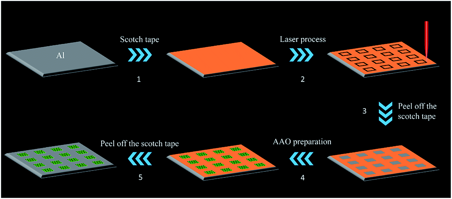
The fabrication of the AAO array detection chip is shown in Fig. 1. We first cut Al foil into an 18 × 18 mm square, and attached Scotch tape on the surface. Then we use a femtosecond laser processing system, as shown in Scheme S1,† to directly write the borders of square units which are arranged into a 4 × 4 grid array on the Scotch tape surface. Afterwards, we peel off the Scotch tape inside the squares to expose the Al foil. Before anodization, the substrate was electropolished in a 1![[thin space (1/6-em)]](https://www.rsc.org/images/entities/char_2009.gif) :7 volume mixture of HClO4 and C2H5OH. After that, porous alumina membranes were prepared in a two-step anodizing process: the substrate after polishing was immersed in a 0.3 mol L−1 oxalic acid electrolyte with Pb as a cathode. The anodizing voltage was maintained at 40 V DC at ambient temperature; after 6 h of anodization, we immerse the substrate in a mixture of 6% phosphoric acid and 1.8% chromic acid at 60 °C for 10 min to remove the aluminum oxide layer, and repeat the first step. Finally, we peel off the remaining Scotch tape to obtain the AAO array detection chip.
:7 volume mixture of HClO4 and C2H5OH. After that, porous alumina membranes were prepared in a two-step anodizing process: the substrate after polishing was immersed in a 0.3 mol L−1 oxalic acid electrolyte with Pb as a cathode. The anodizing voltage was maintained at 40 V DC at ambient temperature; after 6 h of anodization, we immerse the substrate in a mixture of 6% phosphoric acid and 1.8% chromic acid at 60 °C for 10 min to remove the aluminum oxide layer, and repeat the first step. Finally, we peel off the remaining Scotch tape to obtain the AAO array detection chip.
 | ||
| Fig. 1 Schematic for the fabrication of the AAO array-based LOC device. | ||
Surface wettability treatment
The as-prepared AAO detection chip was then immersed in a silver nitrate electrolyte with Al as the cathode under at 1 V DC voltage at ambient temperature (Fig. 2). Electrochemical deposition took place only at the Al foil area outside the AAO regions. After 10 min of electrochemical reaction, the chip was washed with deionized water and dried under a N2 flow. Finally, the chip was immersed in 1′H,1′H,2′H,2′H-perfluorodecanethiol solution (10−3 M in ethanol) for 6 h followed by washing and drying steps.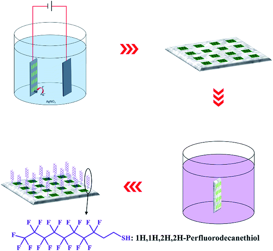 | ||
| Fig. 2 Schematic of the surface wettability treatment process. | ||
Characterization of the fluorescence enhancement properties of the AAO chip
The fluorescence enhancement properties are characterized by using probe molecules R6G at a concentration of 10−6 mol L−1. Each measurement uses 2 μL solution, dropped on both the square area of the AAO chip and Al substrate with the same square area as a reference. Fluorescence spectra of the samples were collected after air drying.Concentration dependent fluorescence spectra of R6G molecules based on the AAO chip
The fluorescence spectra were measured for diluted R6G solutions with concentrations of 10−11, 10−12, 10−13, 10−14, 10−15, 10−16, 10−17 and 0 mol L−1; for the characterization, the data were taken for air dried samples with 2 μL solution. The UV-vis and fluorescence spectra of the R6G liquid sample with different concentrations were collected at the same time.Characterization and measurements
A commercial Ti:sapphire laser system with chirped-pulse-amplification (Spitfire Ace, Spectra Physics, Santa Clara, CA, USA) is employed as a light source for direct laser writing, which delivers horizontally polarized femtosecond laser pulses with a repetition rate of 1 kHz, a central wavelength at 800 nm, and a time duration of 40 fs. The maximum energy of each laser pulse is 7 mJ. Neutral density filters and a half-wave plate were used to control the pulse energy and the direction of the laser polarization, respectively. The laser beam was focused using an objective lens (plan fluorite objective, 4×, N.A = 0.1, f = 17.2 mm, Nikon, Tokyo, Japan) at normal incidence.Confocal fluorescence spectroscopy and mapping analyses were performed with a LabRAM HR Evolution Raman spectrometer (HORIBA Jobin/Yvon) in fluorescence mode with a radiation of 532 nm. The signals were detected with 180° geometry using a multichannel air-cooled (−70 °C) charge-coupled device (CCD) camera. UV-vis spectra of the liquid sample were collected using a Cary 5000 UV-vis-NIR spectrometer (Agilent, USA). Fluorescence spectra of the liquid sample were collected using a Cary Eclipse Bundle (Agilent, USA) with a long life Xe flash lamp and an extended wavelength range PMT (high sensitivity R928) provided as standard. Scanning electron microscope (SEM) characterization was carried out by using an S48000 (Hitachi, Japan), and atomic force microscopy (AFM) characterization was carried out on a MULTIMOD E8 (Bruker, USA). The contact angle (CA) was measured using a POWEREACH JC2000D3 contact angle measurement device. The fluorescence quantum yield was measured using an FL920 fluorescence spectrometer from 528 nm to 700 nm. A Xe lamp was utilized as the excitation light source with a fixed wavelength at 532 nm.
Finite difference time domain method simulations
For the simulations, we have employed the finite-difference-time-domain (FDTD) method based on Yee's algorithms. In the FDTD method, Maxwell's equations are discretized in both time and space. A commercial FDTD package known as Lumerical Solutions (Lumerical Inc.) was used to calculate the electric field distribution of AAO. Perfectly matched layers were used to absorb the scattered radiation in the Z-direction, and periodic boundary conditions were used to perform periodic AAO arrays in X and Y directions. The models are illuminated with a p-polarized plane wave propagating along the Z axis and polarizing along the X axis from the top of AAO. A detector box was placed on the surface to measure the distribution (|Ex|) of the electric field. The source of dipoles was placed on the AAO surface which has different intensities of electric field to analyse the interaction between the molecules and AAO substrate. Ultra-fine mesh sizes (Δx = 1 nm, Δy = 1 nm, Δz = 10 nm) were used in the simulations. A refractive index of n = 1.0 is chosen for air to generate an asymmetric environment. The optical constants of Al and Al2O3 were taken from Palik (Handbook of Optical Constants of Solids).Results and discussion
Surface morphology characterization of the AAO detection chip
The prepared samples are characterized by optical imaging, SEM, and AFM surface morphology analysis, as shown in Fig. 3. As the preparation procedure shown in Fig. 1, after step 2 and step 3, the Scotch tape of the square area was peeled off leaving the Al foil exposed. As a result, during the following polishing and anodization process, remnants of the Scotch tape can prevent the Al foil under the Scotch tape from touching the reagent and all the reactions take place only in the square area. Thus, after polishing and anodization procedures (step 4, Fig. 1), a 2 mm × 2 mm square area AAO array chip was successfully prepared on Al foil spaced 2 mm apart (Fig. 3A).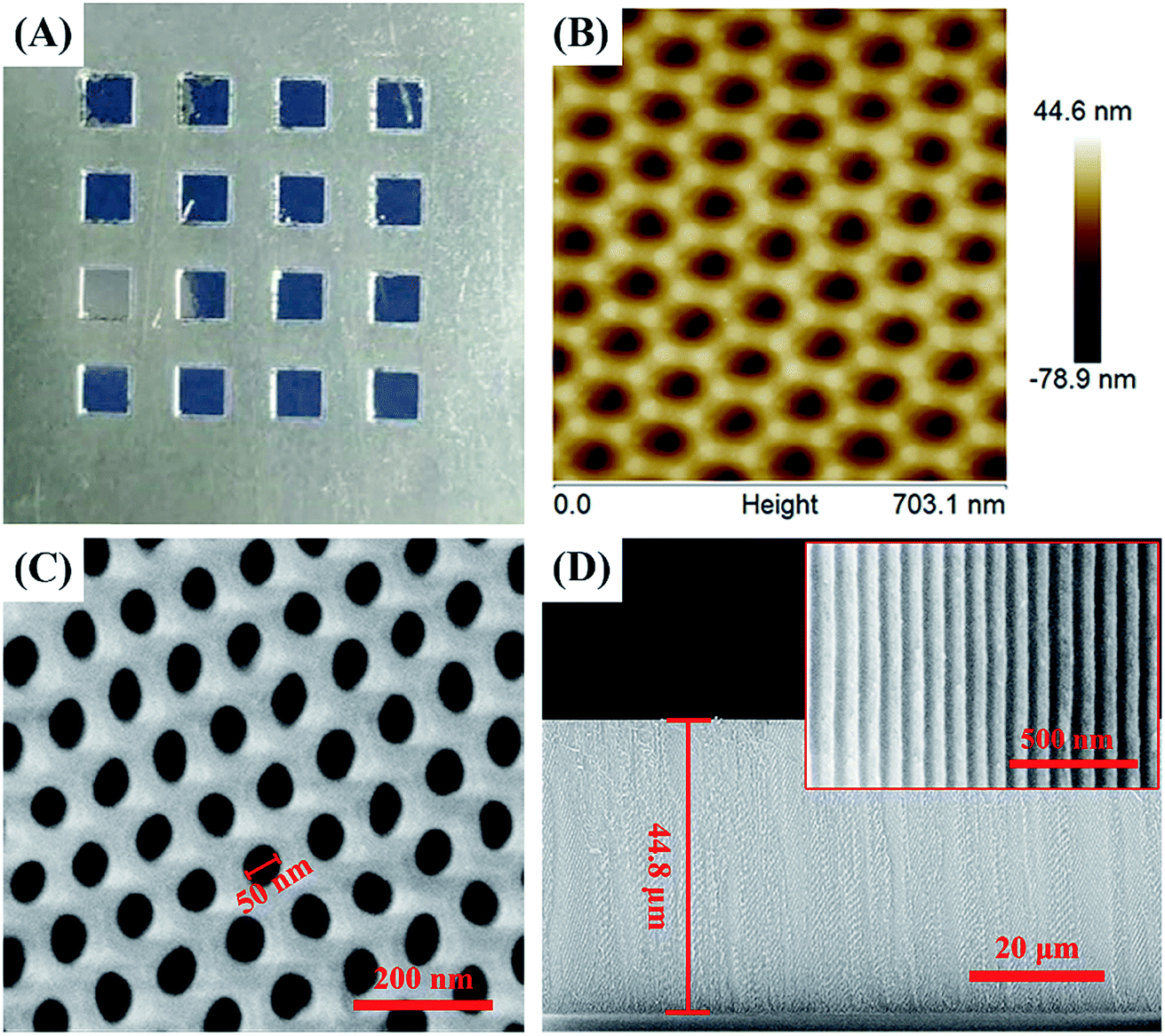 | ||
| Fig. 3 Characterization of the AAO detection array chip: (A) optical image, (B) AFM image, (C) SEM image and (D) the section SEM image of the AAO nanostructures. | ||
Fig. 3B shows the AFM morphology of the AAO nanostructure, which indicates a very uniform nanoporous structure. Fig. 3C and D show the SEM image of the surface and cross section of the AAO nanotemplate. It can be seen from this image that the AAO substrate exhibits a perfectly porous array structure with an average diameter of about 50 nm for each pore. Fig. 3D indicates that the depth of the AAO nanostructure is 44.8 μm. The inset in Fig. 3D shows the amplified figure of the cross section, which is to better observe the structure. It should be mentioned that the depth of the AAO nanopores varied with the oxidation time; the oxidation time used here is 4 h. In addition, the AAO nanoporous template is grown on the base of Al foil, so the nanopores on the upper surface are open, while those on the bottom surface are closed.
Surface wettability treatment and characterization
To increase the detection accuracy and repeatability of this array chip, the Al surface surrounding the AAO units is further hydrophobically treated. This process can ensure that all liquid samples are limited among the AAO units during detection analyses. As shown in Fig. 2, hydrophobic treatment is performed by electrochemically depositing rough Ag nanostructures on the Al foil surface. Due to the high resistance, this procedure does not affect the AAO regions. Electrochemical deposition took place only on the Al foil part and the Ag nanostructure grew in this area. As a result, the surface of Al was covered with a Ag layer. The surface of Al foil is further characterized by SEM and EDS analyses, as shown in Fig. S1;† the surface is covered with rough Ag nanostructures. Then after immersing the substrate in the 1′H,1′H,2′H,2′H-perfluorodecanethiol solution, the sulfhydryl group of this molecule can combine with Ag due to the strong covalent bond between –SH and Ag. This reaction can lead to the modification of 1′H,1′H,2′H,2′H-perfluorodecanethiol on the surface of the Al foil, and decrease the surface energy. Furthermore, the increase of surface roughness can also affect the surface wettability. With such a treatment, the Al foil surface becomes superhydrophobic.The wettability of such a surface is then characterized by a contact angle measurement. Before the measurement, a 2 μL water droplet hanging over the tip of the injector is used to test the wettability by moving towards the Al foil surface and touching and then moving away (Fig. 4A–E). The red arrows show the movement direction. During this process, the droplet is repelled by the Al surface. Thus, the test shows that the hydrophobic treatment gives the surface of the Al foil possesses superhydrophobic properties with extremely low adhesiveness.
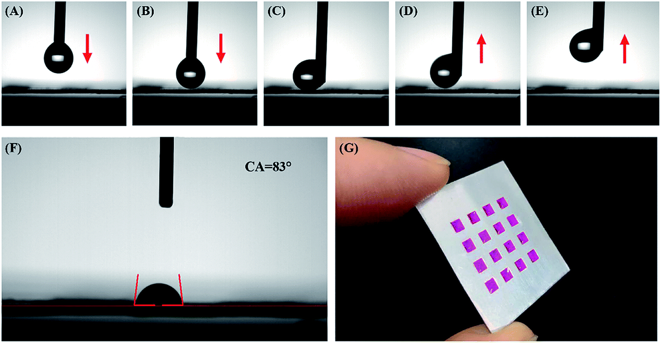 | ||
| Fig. 4 Surface wettability characterization of the Al foil surface after hydrophobic treatment; the arrows label the injector movement direction (A–E), the square AAO substrate (F) and the optical image of the AAO array detection chip with a droplet of 10−3 mol L−1 RhB solution dissolved in water supported on each detection AAO unit (G). | ||
As for the AAO square part, the contact angle measurement result shows a CA = 83° (Fig. 4F), which indicates that AAO has hydrophilic properties with much better adhesiveness than the hydrophobically treated Al foil part. Fig. 4G shows the optical image for the 10−3 mol L−1 RhB solution dissolved in water standing on the AAO units even when the chip is tilted. Therefore, the surface wettability treatment can limit the detection liquid sample to the AAO square area, due to the repellency of its surrounding superhydrophobic Al foil.
Enhanced fluorescence phenomenon on the AAO nanoarray structure
The effect of the AAO nanoarray structure on the fluorescence properties is studied for the R6G molecule (10−6 mol L−1, in water) as a probe molecule. Fig. 5 shows the molecular structure, absorption and fluorescence spectra of R6G molecules.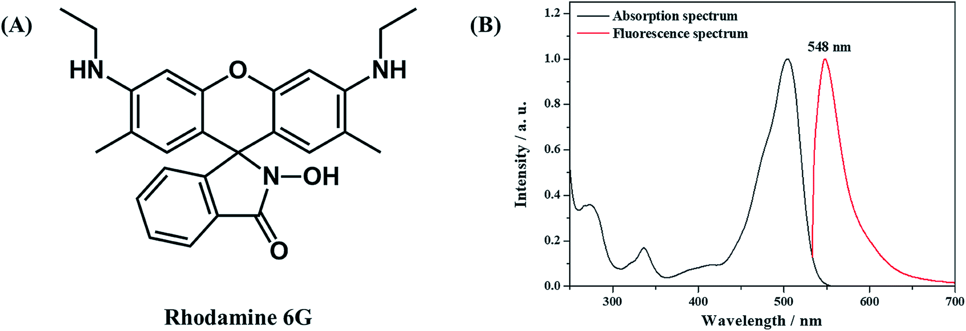 | ||
| Fig. 5 Molecule structure (A) and absorption and fluorescence spectra (B) of R6G molecules. | ||
2 μL solution was dropped on the surface of the AAO square area which is the same amount of molecules dropped on the Al foil with the same area. Confocal fluorescence spectra were then collected. Fig. 6 shows the fluorescence spectra of R6G molecules adsorbed on the AAO substrate and Al foil, under the same conditions. A huge enhancement (70 times by the intensity) is observed and this indicates that AAO with porous nanostructures can enhance the fluorescence intensity of the adsorbed molecules. Fluorescence mapping analyses are also carried out for the R6G molecule adsorbed on the AAO and Al surface in a 30 × 30 μm area, and the results are shown in Fig. 6B and C, separately. The chroma of the mapping result in Fig. 6B is much stronger than that in Fig. 6C, and shows a very uniform color distribution. It indicates that the AAO surface shows very homogeneously enhanced fluorescence properties, which ensure a much better detection accuracy of the AAO substrate.
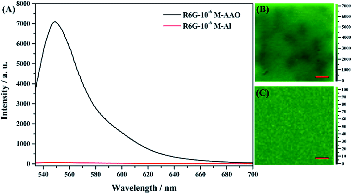 | ||
| Fig. 6 (A) Fluorescence spectra of the molecule adsorbed on the AAO and Al surface. (B) Fluorescence mapping for AAO and (C) Al foil. The scale bar indicates 30 μm. | ||
Effect of the anodization time on the fluorescence enhancement
By controlling the anodization time, the parameters of the porous nanostructures in the AAO substrate can be effectively changed. We try to understand how these parameters affect the fluorescence and to find the best fluorescence enhancement conditions. In the fabrication of the AAO detection chip, we used various second anodization times of 1, 2, 3 and 4 h. From the SEM image of the surface and intersecting surface of the AAO substrate (Fig. S2†), the four substrate samples exhibit nearly the same porous structure with 50 nm diameter, but the thickness of the AAO substrate increases with increasing anodization time.The fluorescence spectra of these four samples are recorded and the results are shown in Fig. 7A. The fluorescence changes with the anodization time, and the substrate prepared with 3 h of anodization shows the strongest enhancement. However, it is also shown from the mapping analyses (in Fig. 7B) that the AAO substrate after 4 h of anodization exhibits the best uniformity. Because the uniformity is much important for achieving a better detection accuracy, we choose 4 h of anodization time as the best substrate preparation conditions for our following studies, though the fluorescence intensity is not the strongest one.
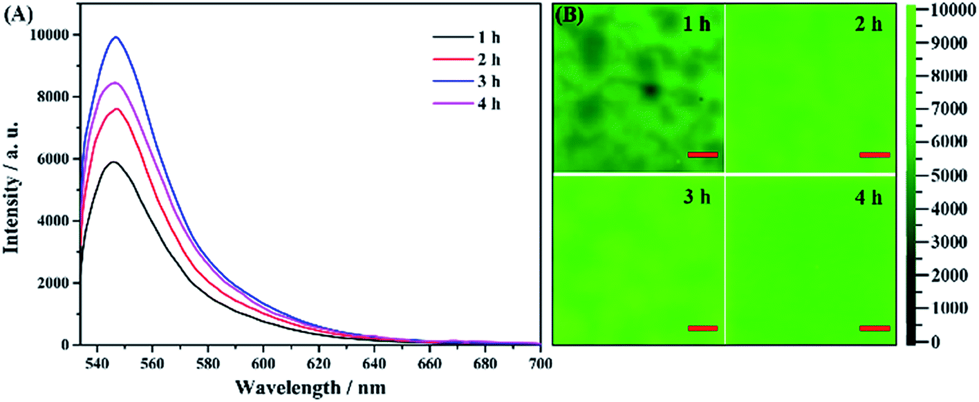 | ||
| Fig. 7 The fluorescence intensity of R6G molecule adsorption on the AAO chip with different anodization times (1, 2, 3 and 4 h) (A) and the mapping analyses of each sample (B). The scale bar indicates 30 μm. | ||
The enhancement mechanism of the AAO nanoporous structures
As previously reported, the enhancement mechanism of the AAO nanostructures was not clearly described. Some attributed the mechanism to the following two reasons: (1) the optical scattering effect of the AAO surface, which causes the redistribution of the electromagnetic fields with high surface intensities, may play a very important role in the fluorescence enhancement;38–40 (2) the fluorescence enhancement might result from the evanescent electrical field or local electromagnetic field enhancement from the surface of the AAO nanoporous structures, observed in metal oxide nanoscale materials.41–44 We believe that both these mechanisms play important roles in the fluorescence enhancement. Thus, to understand the enhancement mechanism, the electromagnetic field distribution of the AAO nanoporous structures was stimulated by the FDTD method, as shown in Fig. 8.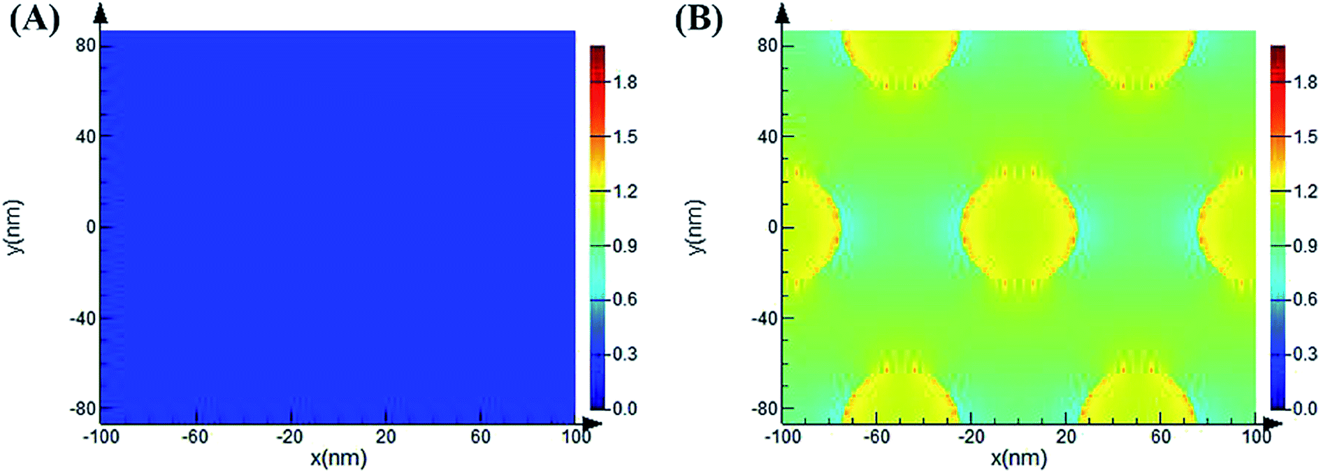 | ||
| Fig. 8 Simulated electromagnetic field distribution of the flat Al surface (A) and AAO nanoporous structures (B) (50 nm, 4 h) by the FDTD method. The incident light wavelength is 532 nm. | ||
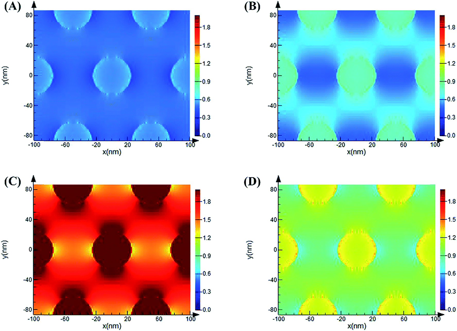
Here, the diameter of the nanopores is 50 nm while the thickness of the template is 44.8 μm (measured from SEM images). The local electromagnetic field enhancement is defined as |E|2/|E0|2 and it can be calculated from the results that the maximum enhancement of the AAO nanopores is about 68 fold that of the Al flat surface. This result is close to the experimental results we obtained. Thus, the enhancement mechanism can be attributed to the local electromagnetic field of the AAO nanoporous structures. The electromagnetic field distribution of R6G molecules, at its maximum emission of 548 nm, adsorbed on the AAO surface at different positions compared to that on the Al surface was further investigated. As Fig. S3† shows, the intensity of R6G molecules on the AAO surface is stronger than that on the flat Al surface. And the intensity distribution is coincident with the electromagnetic field distribution of the AAO nanostructures under the excitation of a 532 nm laser. As calculated from Fig. S3,† the intensity of R6G molecules is 1.1 times stronger than that on the Al surface. This indicates that the AAO nanostructures show no obvious enhancement in the emission of the R6G molecules without the 532 nm excitation laser. Thus, it can be concluded that the fluorescence enhancement mainly arises from the electromagnetic field excited by a 532 nm laser. The simulation of the electromagnetic field distribution of the AAO nanoplate with different thicknesses was further proposed. The results are shown in Fig. 9. As the figure shows, the intensity change of the electromagnetic field with different thicknesses coincides with the experiments shown in Fig. 7.
 | ||
| Fig. 9 Simulated electromagnetic field distribution of AAO nanopores with different thicknesses: (A) 11.2 μm, (B) 22.4 μm, (C) 33.6 μm, and (D) 44.8 μm, by the FDTD method. The incident light wavelength is 532 nm. | ||
To further evaluate the fluorescence enhancement properties, the fluorescence quantum yield (QY) of the Al2O3 + R6G system was obtained. As Fig. S4† shows, the QY of R6G molecules adsorbed on the Al2O3 nanostructures is 18.17% while those on the Al surface hardly show obvious quantum yield results. This is because the light source used in the measurement is a Xe lamp and the photon density is not as strong as the 532 nm laser used in our experiment. Thus, the fluorescence quantum yield of R6G molecules on Al cannot be detected. However, 18.17% QY of R6G molecules adsorbed on Al2O3 indicates that the fluorescence properties of Al2O3 nanostructures can further enhance the QY of the adsorbed molecules.
Concentration dependent enhanced fluorescence analyses
Here we study the detection sensitivity for the fluorescence of the AAO substrate, by varying the R6G molecule concentrations to 10−11, 10−12, 10−13, 10−14, 10−15, 10−16, 10−17 and 0 mol L−1. The results are shown in Fig. 10. As the figure shows, the fluorescence intensity of the R6G molecules adsorbed on the AAO surface increased with increasing concentration of the molecules. The intensity changes logarithmically depending on the concentration, as shown in Fig. 10B, where the fluorescence intensity at 547 nm is plotted as a function of concentration, with a fitting relation Y = −103log(X) + 1776. Obviously, the fluorescence intensity is detectable even when the R6G molecule concentration is 10−17 mol L−1. The sensitivity of the as-synthesized AAO structure can be clearly seen by comparing it with the detection using UV-vis spectra and fluorescence spectra of R6G molecules of the liquid sample collected using a common spectrometer. The UV-vis analysis results of the latter method are shown in Fig. S5,† and the signal is almost not observable when the concentration of R6G molecules decreased to 10−10 mol L−1.
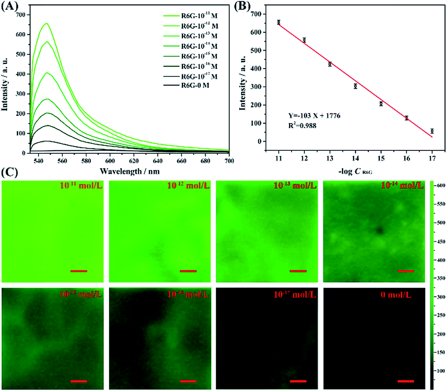 | ||
| Fig. 10 The fluorescence spectra of the R6G molecules adsorbed on the AAO surface with different concentrations (A), fluorescence intensity of R6G molecules with the logarithmic value of R6G molecules (B) and the mapping result with different concentrations of R6G molecules ranging from 10−11 mol L−1 to 0 mol L−1 (C). The scale bar indicates 30 μm. | ||
Meanwhile, the concentration dependent fluorescence spectra of R6G shown in Fig. S6† measured by the fluorescence spectrometer for liquid sample exhibits a 10−9 M detection limit for R6G molecules. It can be thus concluded that the AAO porous nanostructure substrate exhibits obviously enhanced fluorescence properties. Fig. 10C shows the mapping analysis results for the fluorescence detection of R6G molecules adsorbed on each unit. As the figure shows, with the concentration of R6G molecules decreasing, the image color faded, which revealed that the fluorescence intensity of the R6G molecules in the AAO units decreased. Meanwhile, the color of the mapping analysis image is quite uniform for each concentration. This result can further prove that this method is suitable for fluorescence imaging analysis.
Fluorescence detection of the mixture of R6G and RhB
We check the resolvability of the as-synthesized AAO structure for a mixture of molecular components. Fig. 11A shows the fluorescence spectra of R6G and RhB liquid samples with a concentration of 10−6 mol L−1, which were collected using a traditional fluorescence spectrometer. Fig. S7† shows the absorption and fluorescence spectra of RhB molecules. The result shows that under the excitation of 532 nm light, the fluorescence intensity of R6G is much stronger than that of RhB. Meanwhile, 2 μL liquid sample was dropped on the surface of the AAO based detection chip and confocal fluorescence spectral analyses were proposed, as shown in Fig. 11B. It can be clearly found that, based on the AAO detection chip, the fluorescence intensity of RhB is much stronger than that of R6G molecules.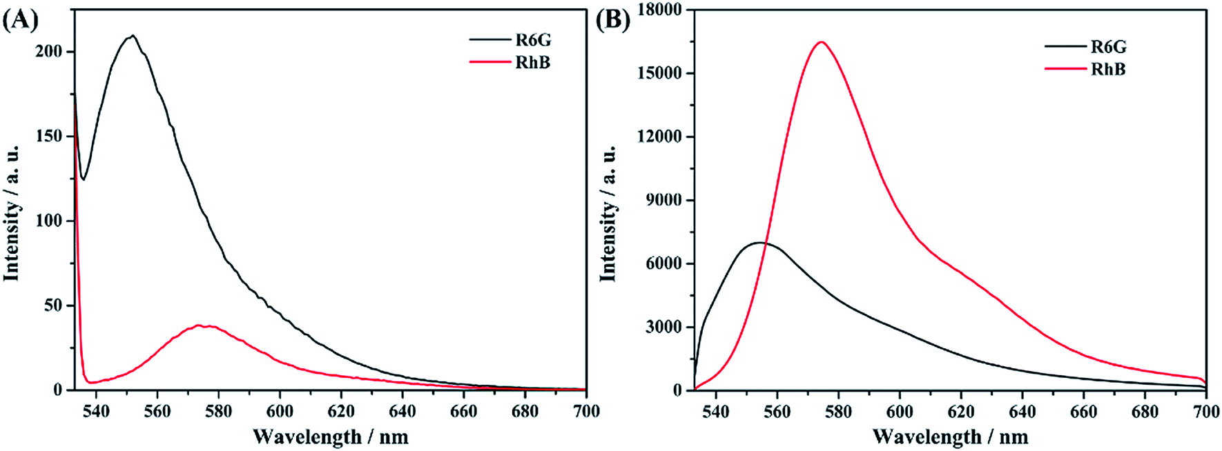 | ||
| Fig. 11 Fluorescence spectra of R6G and RhB solution (A) and confocal fluorescence spectra of R6G and RhB on the AAO chip (B) with the same concentrations. | ||
Thus, we can conclude that the AAO nano pore structure shows much better light amplification of the emission light of RhB molecules at 580 nm than R6G molecules at 547 nm under 532 nm light excitation. It can also been found that, under liquid conditions, the fluorescence signal of R6G molecules covered up the signal of RhB molecules. So, it is too difficult to distinguish the fluorescence signal of RhB molecules from the solution mixture of these two molecules. However, the AAO based confocal fluorescence detection chip possesses much better resolution due to its stronger light amplification of the emission light of RhB at 580 nm. Depending on the above discussion, the detection of RhB molecules from the mixture sample of R6G and RhB with different volume ratios was proposed.
As Fig. 12A shows, the fluorescence spectra of the solution mixture shows an obvious red shift with increasing contents of RhB molecules. This result can be more clearly revealed by the mapping analyses with changing contents of RhB molecules (Fig. 12B). Different colors represent different fluorescence intensities of the spectra. The brightest position (white color) shifts regularly with the change in contents of the RhB molecules, which matches well with the spectral result (Fig. 12A). For comparison, the fluorescence spectra and volume-dependent mapping analysis result of the solution mixture with the same volume ratio were obtained using a traditional fluorescence spectrometer. The results are shown in Fig. S8.† We found from the figure that there is almost no obvious band shift with the change in contents of the RhB molecules. As is well known, the mixture of dye molecules might undergo an energy transfer process, resulting in the enhancement of the fluorescence at very low concentrations. The efficiency of the energy transfer process is strongly distance dependent. Effective FRET was observed in the case of nanocomposites using micelles, films, zeolites and nanofibers as hosts due to the restricted dimensions and spectral overlap between the donor and the acceptor.45–48 In our case, the mixed sample of R6G and RhB was deposited on the surface of the AAO template. The well-ordered nanostructures offer new opportunities for controlling the local environments of the occluded dye molecules. The nanosize pore channel of AAO can restrict the mobility of dye molecules and reduce the distance between the donor and acceptor molecules, which enhanced the energy transfer between R6G and RhB and further increased the recognition of RhB molecules among R6G molecules. Therefore, we can conclude that the AAO based detection chip shows a much better fluorescence resolution for the mixture samples under some specific detection systems, such as R6G and RhB.
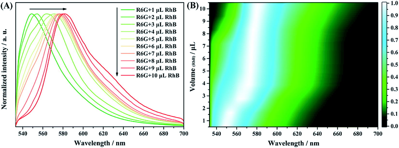 | ||
| Fig. 12 Confocal fluorescence spectra of 100 μL R6G mixed with different volumes of RhB from 1 to 10 μL on the AAO chip (A) and fluorescence mapping analyses of the mixture components (B). | ||
Conclusion
In this paper, we combined the femtosecond laser processing technique and electrochemical anodized oxidation to fabricate array-based fluorescence LOC detection devices with each unit integrated with AAO nanoporous structures. With the assistance of femtosecond laser processing, the integration of AAO nanoporous structural units on a fixed point can be realized. This fabrication method, instead of using conventional photoresists and lithography methods, is much more simple and convenient. The as-prepared LOC devices were used for fluorescence detection analyses and the AAO nanoporous structure shows significant fluorescence enhancement properties with the fluorescence intensity of R6G molecules being enhanced 70 times over a flat surface. Furthermore, the LOC device was found to exhibit a much better spectral resolution than traditional fluorescence spectrometers in liquid samples, based on which the mixture of R6G with different contents of RhB molecules can be obviously distinguished using the fluorescence emission band shifts with changing contents of RhB molecules. Thus, the as-prepared array based LOC device is not only suitable for fluorescence enhancement analyses but also beneficial for the detection of mixture components.Conflicts of interest
There are no conflicts to declare.Acknowledgements
This research was supported by the National Key R&D Program of China (2017YFB1104700), the National Natural Science Foundation (NSFC, Grant no. 61705227, 61774155, 11774340), the Jilin Provincial Science & Technology Development Project (20180414019GH), and the Scientific research project of the Chinese Academy of Sciences (QYZDB-SSW-SYS038).References
- A. Manz, N. Graber and H. M. Widmer, Sens. Actuators, B, 1990, 1, 244–248 CrossRef CAS.
- F. F. Bier and S. Schumacher, Adv. Biochem. Eng./Biotechnol., 2013, 133, 1–14 CrossRef CAS PubMed.
- D. Figeys and D. Pinto, Anal. Chem., 2000, 72, 330a–335a CrossRef CAS PubMed.
- J. Kong, L. Jiang, X. O. Su, J. H. Qin, Y. G. Du and B. C. Lin, Lab Chip, 2009, 9, 1541–1547 RSC.
- Y. Zhang, H. Yu, J. H. Qin and B. C. Lin, Biomicrofluidics, 2009, 3, 044105 CrossRef PubMed.
- C. Y. Li, X. L. Dong, J. H. Qin and B. C. Lin, Anal. Chim. Acta, 2009, 640, 93–99 CrossRef CAS PubMed.
- Y. X. Li, Y. Q. Li, B. Zheng, L. L. Qu and C. Li, Anal. Chim. Acta, 2009, 643, 100–107 CrossRef CAS PubMed.
- D. Mark, S. Haeberle, G. Roth, F. von Stetten and R. Zengerle, Chem. Soc. Rev., 2010, 39, 1153–1182 RSC.
- H. Craighead, Nature, 2006, 442, 387–393 CrossRef CAS PubMed.
- D. G. Grier, Nature, 2003, 424, 810–816 CrossRef CAS PubMed.
- S. K. Sia and G. M. Whitesides, Electrophoresis, 2003, 24, 3563–3576 CrossRef CAS PubMed.
- M. T. Breckenridge, T. T. Egelhoff and H. Baskaran, Biomed. Microdevices, 2010, 12, 543–553 CrossRef PubMed.
- D. Irimia and M. Toner, Integr. Biol., 2009, 1, 506–512 CrossRef CAS PubMed.
- S. N. Bhatia and D. E. Ingber, Nat. Biotechnol., 2014, 32, 760–772 CrossRef CAS PubMed.
- K. Sugioka and Y. Cheng, Appl. Phys. Rev., 2014, 1, 041303 Search PubMed.
- K. C. Phillips, H. H. Gandhi, E. Mazur and S. K. Sundaram, Adv. Opt. Photonics, 2015, 7, 684–712 CrossRef CAS.
- B. Gu, Proc. Soc. Photo-Opt. Instrum. Eng., 2004, 5339, 226–230 CrossRef.
- R. Buividas, M. Mikutis, T. Kudrius, A. Greicius, G. Slekys and S. Juodkazis, Lith. J. Phys., 2012, 52, 301–311 CrossRef CAS.
- N. Sudani, K. Venkatakrishnan and B. Tan, Optic Laser Eng., 2009, 47, 850–854 CrossRef.
- B. N. Chichkov, C. Momma, S. Nolte, F. vonAlvensleben and A. Tunnermann, Appl. Phys. A: Mater. Sci. Process., 1996, 63, 109–115 CrossRef.
- K. Sugioka and Y. Cheng, Lab Chip, 2012, 12, 3576–3589 RSC.
- Y. L. Zhang, Q. D. Chen, H. Xia and H. B. Sun, Nano Today, 2010, 5, 435–448 CrossRef CAS.
- C. B. Schaffer, A. Brodeur and E. Mazur, Meas. Sci. Technol., 2001, 12, 1784–1794 CrossRef CAS.
- R. R. Gattass and E. Mazur, Nat. Photonics, 2008, 2, 219–225 CrossRef CAS.
- R. Osellame, G. Cerullo and R. Ramponi, Femtosecond laser micromachining: photonic and microfluidic devices in transparent materials, Springer, Berlin, 2012 Search PubMed.
- C. H. Lin, L. Jiang, H. Xiao, S. J. Chen and H. L. Tsai, Opt. Lett., 2010, 35, 2937–2939 CrossRef CAS PubMed.
- J. Xu, D. Wu, Y. Hanada, C. Chen, S. Z. Wu, Y. Cheng, K. Sugioka and K. Midorikawa, Lab Chip, 2013, 13, 4608–4616 RSC.
- C. G. K. Malek, Anal. Bioanal. Chem., 2006, 385, 1362–1369 CrossRef PubMed.
- K. Sugioka, J. Xu, D. Wu, Y. Hanada, Z. K. Wang, Y. Cheng and K. Midorikawa, Lab Chip, 2014, 14, 3447–3458 RSC.
- A. Chen, M. M. Eberle, E. J. Lunt, S. Liu, K. Leake, M. I. Rudenko, A. R. Hawkins and H. Schmidt, Lab Chip, 2011, 11, 1502–1506 RSC.
- X. Fang, Q. Q. Zhao, H. M. Cao, J. Liu, M. Guan and J. L. Kong, Analyst, 2015, 140, 7823–7826 RSC.
- A. Banerjee, A. Pais, I. Papautsky and D. Klotzkin, IEEE Sens. J., 2008, 8, 621–627 CAS.
- P. A. Quinto-Su, H. H. Lai, H. H. Yoon, C. E. Sims, N. L. Allbritton and V. Venugopalan, Lab Chip, 2008, 8, 408–414 RSC.
- S. Kuhn, B. S. Phillips, E. J. Lunt, A. R. Hawkins and H. Schmidt, Lab Chip, 2010, 10, 189–194 RSC.
- R. P. Jia, Y. Shen, H. Q. Luo, X. G. Chen, Z. D. Hu and D. S. Xue, Thin Solid Films, 2005, 471, 264–269 CrossRef CAS.
- R. Q. Li and H. Grebel, IEEE Sens. J., 2010, 10, 465–468 CAS.
- M. L. Wang, G. W. Meng, Q. Huang, M. T. Li, Z. B. Li and C. L. Tang, Analyst, 2011, 136, 278–281 RSC.
- T. Fujii, Y. Gao, R. Sharma, E. L. Hu, S. P. DenBaars and S. Nakamura, Appl. Phys. Lett., 2004, 84, 855–857 CrossRef CAS.
- T. H. Zhang, Y. He, J. J. Wei and L. Que, Biosens. Bioelectron., 2012, 38, 382–388 CrossRef CAS PubMed.
- N. Ganesh, W. Zhang, P. C. Mathias, E. Chow, J. A. N. T. Soares, V. Malyarchuk, A. D. Smith and B. T. Cunningham, Nat. Nanotechnol., 2007, 2, 515–520 CrossRef PubMed.
- A. Dorfman, N. Kumar and J. I. Hahm, Langmuir, 2006, 22, 4890–4895 CrossRef CAS PubMed.
- J. W. Zhao, L. Z. Wu and J. F. Zhi, J. Mater. Chem., 2008, 18, 2459–2465 RSC.
- C. P. Gu, J. R. Huang, N. Ni, M. Q. Li and J. H. Liu, J. Phys. D: Appl. Phys., 2008, 41, 175103 CrossRef.
- H. Wang, Z. Yin, W. Xu, D. L. Zhou, S. B. Cui, X. Chen, H. N. Cui and H. W. Song, Nanoscale, 2016, 8, 10004–10009 RSC.
- C. V. Kumar and A. Chaudhari, Microporous Mesoporous Mater., 2000, 41, 307–318 CrossRef CAS.
- B. J. Scott, M. H. Bartl, G. Wirnsberger and G. D. Stucky, J. Phys. Chem. A, 2003, 107, 5499–5502 CrossRef CAS.
- K. J. Lee, J. H. Oh, Y. Kim and J. Jang, Adv. Mater., 2006, 18, 2216–2219 CrossRef CAS.
- L. Z. Wang, Y. L. Liu, F. Chen, J. L. Zhang and M. Anpo, J. Phys. Chem. C, 2007, 111, 5541–5548 CrossRef CAS.
Footnote |
| † Electronic supplementary information (ESI) available. See DOI: 10.1039/c9na00352e |
| This journal is © The Royal Society of Chemistry 2019 |