
 Open Access Article
 This Open Access Article is licensed under a Creative Commons Attribution-Non Commercial 3.0 Unported Licence
Controlling the degrees of freedom in metasurface designs for multi-functional optical devices
Bo
Xiong
ab,
Lin
Deng
c,
Ruwen
Peng
*b and
Yongmin
Liu
 *ac
*ac
aDepartment of Mechanical and Industrial Engineering, Northeastern University, Boston, Massachusetts 02115, USA. E-mail: y.liu@northeastern.edu
bNational Laboratory of Solid State Microstructures, School of Physics, Collaborative Innovation Center of Advanced Microstructures, Nanjing University, Nanjing 210093, China. E-mail: rwpeng@nju.edu.cn
cDepartment of Electrical and Computer Engineering, Northeastern University, Boston, Massachusetts 02115, USA
First published on 2nd September 2019
Abstract
This review focuses on the control over the degrees of freedom (DOF) in metasurfaces, which include the input DOF (the polarization, wavelength and incident angle of the input light and some dynamic controls), parameter DOF (the complex geometric design of metasurfaces) and output DOF (the phase, polarization and amplitude of the output light). This framework could clearly show us the development process of metasurfaces, from single-functional to multi-functional ones. Advantages of the multi-functional metasurfaces are discussed in the context of various applications, including 3D holography, broadband achromatic metalenses and multi-dimensional encoded information. By combining all the input and output DOF together, we can realize ideal optical meta-devices with deep subwavelength thickness and striking functions beyond the reach of traditional optical components. Moreover, new research directions may emerge when merging different DOF in metasurfaces with other important concepts, such as parity-time symmetry and topology, so that we can have the complete control of light waves in a prescribed manner.
1. Introduction
Metasurfaces,1–15 two-dimensional metamaterials with planar and ultrathin nanostructures, have shown exceptional abilities in light manipulation and versatility in optical applications.7,16–20 In contrast to conventional freeform optical devices that are normally bulky, metasurfaces offer fundamentally new methods to control the phase, amplitude, and polarization of light from the re-radiation of subwavelength structures upon illumination.8,21,22 Such a strategy can dramatically decrease the weight and size of optical components, enabling miniaturization and integration for on-chip optical systems.23–26 By judiciously engineering the geometric parameters of subwavelength structures, including the width,27 thickness28 and orientation,29 we can design a variety of metasurfaces to manipulate optical waves in an prescribed manner. Many exotic phenomena, such as polarization multiplexing30–33 and broadband achromatic responses,34–36 which are difficult to achieve with natural materials, have been demonstrated using metasurfaces. In addition, conventional optical elements are typically designed to achieve one single functionality, while multi-functional devices are highly desired for modern photonic applications. With the rapid development of design methodology and nanofabrication technology, metasurfaces that encode multiple functions within a single platform have been successfully demonstrated.11,14,25 Here, we would like to present one distinct design framework based on DOF and provide a comprehensive viewpoint to understand the recent developments of metasurfaces that have evolved from single-dimension to multiple-dimensions in the functionality space.As schematically shown in Fig. 1, the DOF in the metasurface design space can be divided into three parts, including the input, parameter and output DOF, respectively. The input DOF means the initial conditions of the metasurface system, which contains the basic properties of incident light and the active parameters for dynamic controls. This part mainly describes under which conditions a specific metasurface operates. As for the parameter DOF, it is about how to properly design the geometric parameters of the building blocks of metasurfaces and how to arrange them in two-dimensional space. Once the incident condition and the complex design of a metasurface are fixed, the output DOF of radiated electromagnetic waves, including the phase, amplitude and polarization modulation, could be determined.
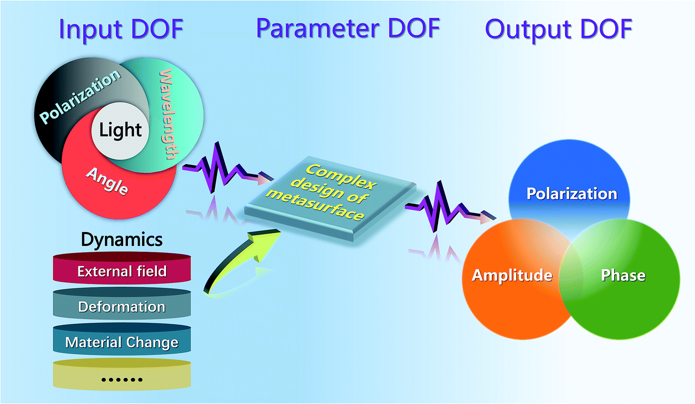 | ||
| Fig. 1 Schematic of DOF in metasurface designs. The input DOF includes the properties of incident light and working conditions. The output DOF corresponds to the properties of re-radiated light. By controlling the parameter DOF of the complex metasurface, the desired properties and functionalities of output signals can be realized. | ||
This review article is organized as follows. In Section 2, we will introduce some simple cases of metasurfaces, which can be regarded as a mapping from one input DOF to one output DOF. In Section 3, more complicated metasurfaces with the ability to simultaneously control multiple properties of output light will be discussed. In Section 4, 5 and 6, we will review multiplexed metasurfaces that can realize multiple functions depending on different DOF of input light, like incident angle and polarization. Dynamic metasurfaces, one important subarea aiming to achieve tunable and reconfigurable functionalities, will be discussed in Section 7. In Section 8, we will focus on controlling multiple output DOF with multiple input DOF. This case is the most complicated but also the most fascinating one. Finally, in Section 9, we provide concluding remarks and an outlook on future directions.
2. Simple cases of metasurfaces
Phase is one of the most fundamental properties of light, in addition to the amplitude, and polarization. A phase modulation range of 2π is necessary to provide full control of the wavefront. However, if only one single Lorentz resonance is involved in a meta-atom, i.e., the building block of a metasurface, the tuning range of the phase is up to π.21 In 2011, Capasso's group proposed the generalized laws of reflection and refraction with a linear phase variation along the ultrathin interface between two media,1,37 as illustrated in Fig. 2a. This is the first successful experimental demonstration for the ability to achieve a phase coverage of 2π in the mid-infrared region, thanks to the two different plasmonic eigenmodes that arise from the distinct distributions of induced currents. V-shaped metallic structures with different opening angles and orientation angles are designed to have equal phase difference dφ = π/4 between eight neighboring building blocks. Such 8-level phase discretization provides great flexibility in the control of light beams, for instance, the generation of optical vortices by planar designer metallic interfaces. The V-shaped structures are arranged helicoidally into eight regions (Fig. 2b) to generate a phase shift that varies azimuthally from 0 to 2π, thus producing an optical vortex (Fig. 2c). If we classify this seminal work into the design framework shown in Fig. 1, the incident condition can be regarded as linear polarized light with normal incidence. By carefully tuning the geometry shape and size, the operating wavelength can be readily changed. In 2012, Ni et al. demonstrated that in the near-infrared, V-shaped gold antennas with 30 nm thickness can also provide a tunable phase delay from 0 to 2π.15 The anomalous reflection and refraction can be observed for wavelengths from 1.0 to 1.9 μm, which means a broadband effect existing in this system. Besides single-layer V-shaped antennas, metal-insulator-metal (MIM) structures have also been applied to realize full phase modulation in the reflection configuration.38–41 The metallic nanostructure on the top layer can be patch39 or H-shaped.38 When the MIM structure is illuminated by the incident light polarized along one specific direction, electric resonance will be induced on both the nanostructure and the ground plane. Because the two layers are very close to each other, the strong near-field coupling can create a magnetic resonance. In this system, the geometrical and material parameters of the nanostructure would affect this magnetic resonance and efficiently tune the reflection phase delay of each unit structure. The MIM design can overcome several disadvantages of the single-layer V-shaped antennas, including operation limit on cross-polarized light and low conversion efficiency.39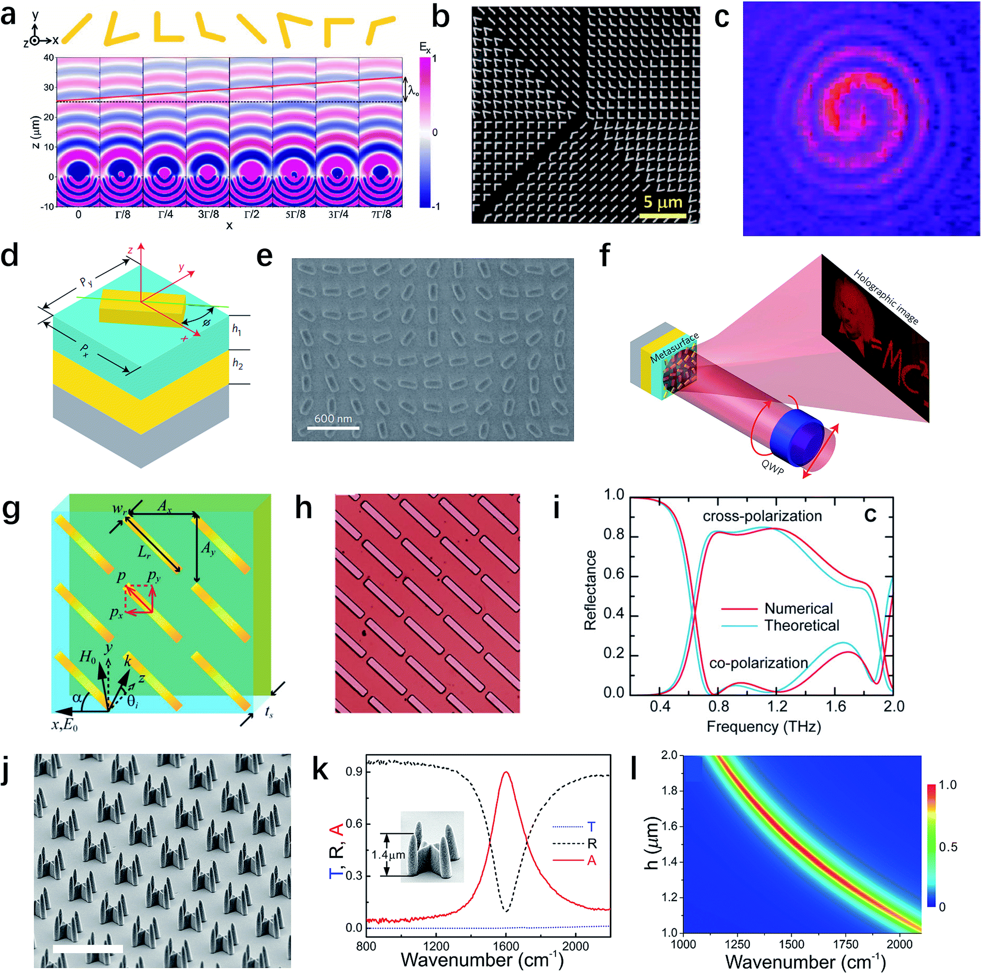 | ||
| Fig. 2 Metasurfaces for the single property modulation of output light. (a) Wavefront distribution of the scattered electric field for V-shaped antennas with different geometries. (b) SEM image and (c) measured spiral patterns of the vortex metasurfaces composed of eight regions with different antennas. (d) Schematic of the unit cell and (e) SEM image of the fabricated MIM metasurfaces sample. (f) Illustration of the reflective computer-generated hologram under a circularly polarized incident beam. The reflected beam forms the holographic image in the far field. (g) Schematic and (h) optical microscopy image of the metamaterial-based terahertz polarization converter, whose performance is shown by the numerically simulated and theoretically calculated reflection spectra for cross-polarized and co-polarized light in (i). (j) SEM image of the perfect absorber composed of periodic four-tined fish-spear-like resonators. The scale bar is 5 μm. (k) The measured transmission (T), reflection (R) and absorbance (A) spectra for the sample with a height of 1.4 μm. (l) The simulated absorbance spectrum for different spear heights. (a–c) Reproduced with permission.1 (d–f) Reproduced with permission.29 (g–i) Reproduced with permission.56 (j–l) Reproduced with permission.74 | ||
In addition to introducing multiple resonances of various plasmonic nanoantennas, we can use a strikingly different approach to achieve complete 2π phase modulation by using the so-called Pancharatnam–Berry (PB) phase. It is a geometric phase for left-circularly polarized (LCP) or right-circularly polarized (RCP) light that can be readily achieved via spatially rotating each unit cell.42–45 Compared with phase modulation enabled by resonant structures, PB phase is not subject to dispersion, and hence can generate dispersionless phase discontinuities to control light propagation.46 In this design approach, the phase delay solely depends on the orientation of metallic rod antennas, rather than their spectral responses and the wavelength of the incident light. By arranging the antennas with different rotation angles along the interface, the phenomenon of broadband anomalous refraction has been observed in the visible region. Besides rod nanoantennas, rectangular apertures47 and U-shaped apertures48 can also support the similar effect of phase modulation, which work as anisotropic scatters and provide different scattering coefficients for incident light linearly polarized along two directions.3 However, to realize a high-efficiency PB phase metasurface, the Jones matrix of an anisotropic scatterer should be the same as that of a half wave plate. Zheng et al. demonstrated that by properly choosing the length, width and thickness of Au nanorods (Fig. 2d), the phase difference between the reflection coefficients rl (along the long axis) and rs (along the short axis) approaches π within a wide wavelength range of 600–1000 nm.29 In the meantime, the configuration maintains very large reflection amplitudes over 80% for both linear polarizations. This forms the basis of the high-efficiency geometric metasurfaces. The scanning electron microscope (SEM) image of the fabricated sample and the experimental results are shown in Fig. 2e and f, respectively. A computer-generated hologram with 16-level-phase has been demonstrated for a circularly polarized beam. The diffraction efficiency reaches as high as 80% at 825 nm, making the strategy viable for various practical holographic applications, while it is limited to operation in the reflection mode. To achieve high efficiencies in transmission mode in the visible spectrum, in 2014, Brongersma's group described the experimental realization and operation of dielectric gradient metasurfaces.49 For high-index dielectric nanoantennas, ohmic loss in the metal and the limited scattering cross sections can be avoided, which tremendously increases the transmission efficiency.6,50–54
Polarization is another intrinsic property of electromagnetic waves conveying valuable information in signal transmission and sensing measurements. Conventionally, polarization control utilizes the effect of birefringence or total internal reflection55 in crystals and polymers, giving rise to phase retardation between the two orthogonally polarized wave components. However, this method has limitations of narrow frequency band and low efficiency. Grady et al. have recently demonstrated an ultrathin and broadband terahertz polarization converter, which is capable of rotating a linear polarization state to the orthogonal one in the reflection configuration with high efficiency.56 As Fig. 2g and h show, the converter consists of an array of metallic cut-wires and a metal ground plane separated by a dielectric spacer layer. The interference in the multi-reflection process can enhance the overall amplitude of cross-polarized light. This concept is validated by full-wave numerical simulations presented in Fig. 2i. In the frequency range from 0.8 and 1.36 THz, the reflection of cross-polarization is higher than 80%, and the co-polarized one is below 5%, representing a broadband and efficient linear polarization converter in the reflection configuration. Notably, there is a transmission-type polarization converter using a tri-layer metasurface, whose efficiency is also higher than 80%.57 A nearly perfect orthogonal polarization conversion has been experimentally observed. Further investigations demonstrated that a freely tunable polarization rotator can be realized in broadband THz range with a three-rotating-layer metallic grating structure.58 This device can conveniently convert a linearly polarized THz wave to any desired polarization direction with almost perfect conversion efficiency, which has a wide range of applications in analytical chemistry, sensing, imaging, communication technology, etc. In addition to polarization converters working in THz, ultrathin quarter-wave plates37,59,60 and half-wave plates61–63 based on plasmonic metasurfaces have also been designed to manipulate light polarization in the infrared and visible. Compared with traditional wave plates, metasurface can support ultra-broadband responses and background free performances.37
The last output DOF listed in Fig. 1 is the amplitude of electromagnetic waves. One interesting application for amplitude modulation is the Fresnel zone plate,64 which consists of a set of radially alternating rings with opaque and transparent properties. Light incident on a zone plate will diffract around the opaque zones and constructively interferes at the desired focus, resulting in focusing and imaging.65–67 Besides the zone plate, another important device is metamaterial-based absorbers,68–75 which have important applications in sensors, thermal imaging, and so on. The idea of perfect absorbers was proposed for the first time by Landy et al., who demonstrated absorbance greater than 88% at 11.5 GHz.76 Composed of two resonators that couple separately to the electric and magnetic components of the incident field, the structure can absorb all incident radiation with near unity absorbance. Since then, various absorber structures have been designed for frequencies ranging from microwave77,78 to terahertz (THz),79,80 infrared69,81,82 and even optical frequencies.83 However, most of these designs use MIM structures, in which the heat generation inside the structures causes some problems such as ultrafast heating, surface melting, and reshaping. To solve these issues, Peng's group reported a new type of absorber constructed with four-tined fish-spear-like resonators (FFRs) as shown in Fig. 2j.74 Each FFR can be regarded as the combination of two cross-standing, identical U-shaped resonators, covered by a metallic thin film. Instead of generating strong local fields inside a dielectric interlayer in MIM structures, the electric fields occur in the air region between the tines of FFRs. More than that, the continuous metallic thin film plays the role of a perfect thermal and electric conductor, increasing the in-plane thermal diffusion. The measured spectra in Fig. 2k show that for FFRs with height of 1.4 μm, the reflection possesses a clear valley at 1400 cm−1, while the transmission remains almost zero (less than 0.5%) over the spectral regime from 800 to 2200 cm−1. Therefore, the absorbance reaches 99.3% at 1400 cm−1, which approaches perfect absorption. Furthermore, by varying the height from 1.3 to 1.8 μm, the wavenumber of the maximum absorbance can be tuned from 1300 to 1700 cm−1 while the absorbance remains more than 95% (Fig. 2l).
3. Simultaneous control of multiple properties of output light in metasurfaces
In the previous section, we have introduced the basic function of metasurfaces in manipulating the single property of output light, including the phase, polarization and amplitude. For certain important applications, such as holography, beam shaping, and construction of complex wave fields, simultaneous control over both amplitude and phase is required. In traditional holography, the phase modulation relies on light propagation inside the material to accumulate phase, which means the thickness of phase holograms is usually comparable to or larger than the wavelength. In 2013, Ni et al. proposed an ultra-thin metasurface hologram with a thickness of only 30 nm.84 In this design, the Babinet-inverted, complementary nanoantennas can provide simultaneous amplitude and phase modulation, which generate high-resolution and low-noise holographic images in the visible wavelength range. However, due to the complexity required in designing the antenna geometry, the phase and amplitude were limited to only a few discrete levels. Subsequently, Zhang's group designed a metasurface consisting of C-shaped antennas,85 as shown in Fig. 3a, in which the phase modulation is determined by the geometrical configuration of each antenna, and the amplitude control is realized by rotating the structure. Therefore, nearly arbitrary complex transmission/reflection coefficients can be locally controlled at the interface. To experimentally demonstrate the analysis, the authors have fabricated one sample (Fig. 3b) to achieve two diffraction orders, for which the theoretical amplitude and phase distributions are shown in Fig. 3c. From the measured results, two diffraction orders are clearly seen over the frequency range of 0.8 to 1.0 THz (Fig. 3d). This approach represents a facile and robust way to obtain a metasurface with simultaneous phase control and continuously tunable amplitude profile. Using the similar design principle, Wang et al. have demonstrated several longitudinal manipulations of the holographic images, including shifting, stretching and rotating.86 Dielectric cubic silicon resonators are used to implement multi-level modulation of both the amplitude and phase in the terahertz regime, and the Rayleigh–Sommerfeld diffraction theory is applied in their design. Fig. 3e shows the electric field amplitude and phase distributions of the meta-hologram. Fig. 3f and g are the simulated and measured amplitude distributions of the electric field, respectively, at different locations along the z-axis, the propagation direction. The rotating manipulation of the image can be clearly seen with good quality. The proposed meta-holograms offer more freedom in holographic designs and open new avenues towards complex three-dimensional holography.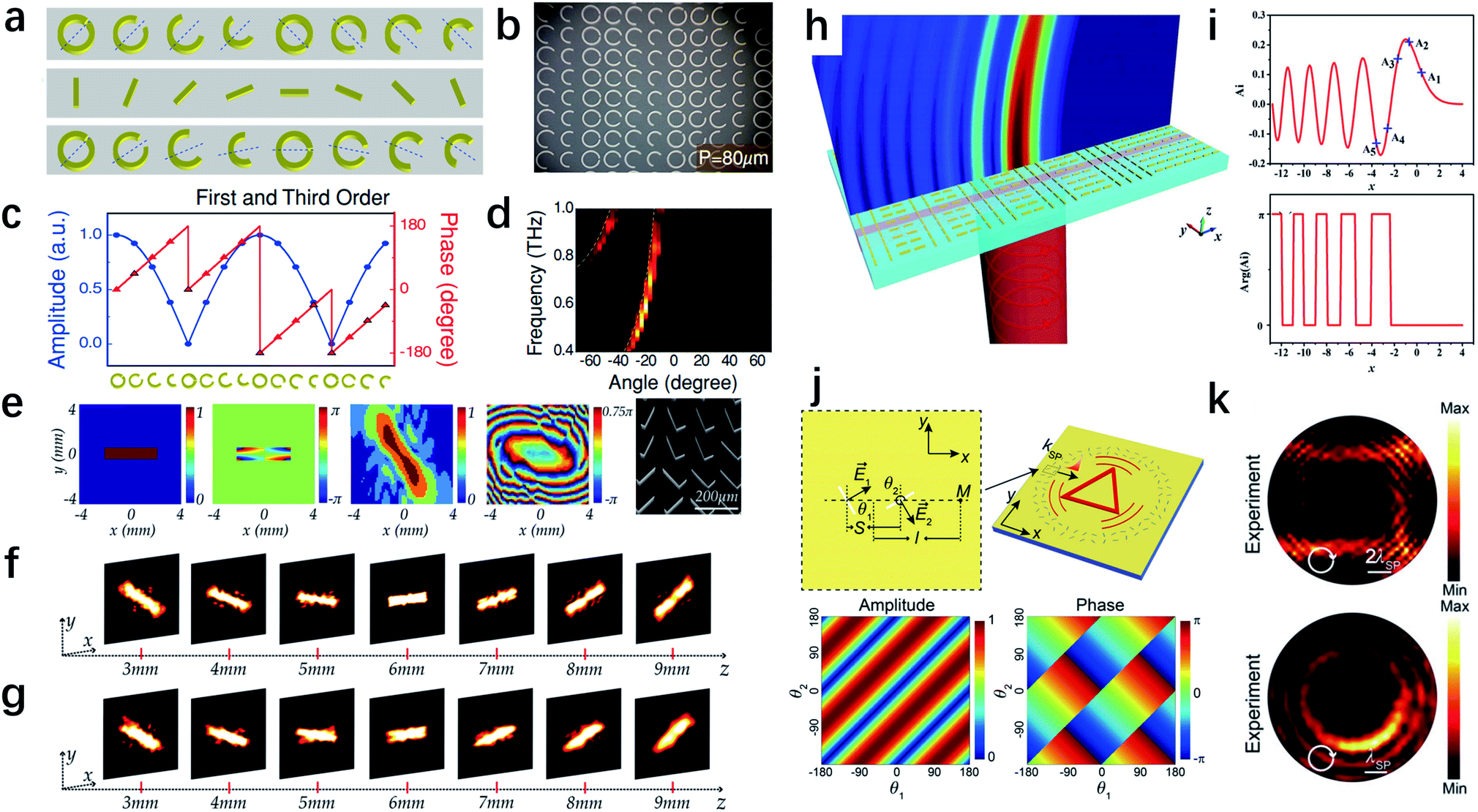 | ||
| Fig. 3 Metasurfaces for simultaneous control of phase and amplitude. (a) Schematic and (b) optical image of the metasurfaces, in which geometrical parameters are designed for the phase control and orientation angles are varied for the amplitude control. (c) Designed amplitude and phase profiles for the sample to achieve two diffraction orders and (d) the measured diffraction pattern. (e) The amplitude and phase distributions for the holographic image and the corresponding design and SEM image for a meta-hologram. (f) Simulated and (g) measured amplitude distributions of the holographic image at different locations along the z-axis. (h) Illustration of generating the Airy beam from a plasmonic metasurface. (i) The amplitude and phase pattern of a normalized Airy function. (j) Design of the unit cell and the calculated amplitude and phase for different orientation angles of a pair of slit apertures. (k) Experimental results of square-shaped and nonuniform circle-shaped SP profiles, respectively. (a–d) Reproduced with permission.85 (e–g) Reproduced with permission.86 (h and i) Reproduced with permission.90 (j and k) Reproduced with permission.101 | ||
Another example of simultaneous control of phase and amplitude is the manipulation of Airy beams,87–89 which have attracted considerable research interest for their unique properties, such as non-diffraction, self-healing, and self-bending in the absence of any external potential. As shown in Fig. 3h, a simplified metasurface with orthogonal nanorods has been employed to realize Airy beams with simultaneous phase and amplitude modulation.90 The phase shift of the scattering light can be controlled by the orientation of nanorods while the amplitude can be determined by the length of nanorods. The simulation results in Fig. 3i show the oscillatory phase pattern and exponential decay amplitude distribution along the x-axis, which demonstrate great consistency with the typical Airy beam.
The strategy of simultaneous control can also be used to manipulate the propagation of surface plasmons (SP) and generate arbitrary SP profiles.91–93 SPs arise from the collective oscillation of electrons excited by photons, and behave as optical surface waves propagating at a metal–dielectric interface. While metasurfaces have successfully demonstrated a number of applications including subdiffractional lithography,94,95 SP metalenses,93,96,97 and unidirectional launchers,98–100 most of these works focus on realizing simple SP profiles with a phase-only design. Nevertheless, it is desirable to generate more complex SP profiles, which promise opportunities for practical plasmonic applications such as surface displays. For this reason, Xu et al. proposed that an arbitrary profile of the excited SP can be achieved utilizing simultaneous control of phase and amplitude.101 In Fig. 3j, the simulated results show that by varying the rotation angles θ1 and θ2, paired slit resonators can generate SPs with any combination of phase and amplitude. Using this strategy, two specific SP patterns, including a square-shaped profile and a circle-shaped profile with nonuniform intensity distribution, have been demonstrated in experiments as shown in Fig. 3k.
Apart from phase and amplitude, novel phenomena can also be induced from simultaneous control of polarization and phase especially in vectorial optics.102 Traditional methods to realize the simultaneous control requires a combination of multiple discrete optical components like cascaded structures,103 imposing challenges to further scale down the system to meet the requirement in practical applications. Fig. 4a shows a new kind of dual-layer plasmonic metasurfaces that can simultaneously control the phase and polarization of the transmitted light.104 The phase is controlled by varying the geometric parameters, while the polarization is filtered by rotating the rectangular nano-apertures, since only optical component along the major axis can transmit through the structure for a circularly-polarized incident beam. In experiments, thirty-six nano-aperture pairs are designed (Fig. 4b), realizing a 6-level phase and amplitude modulation. The experimental results for the sample in Fig. 4c show excellent consistency with the profile of a regular polarized beam (Fig. 4d). However, the plasmonic metasurface exhibits only 30% efficiency for linearly polarized incidence at 900 nm. To reduce ohmic losses in plasmonic metasurfaces and improve efficiency, dielectric designs105,106 have been introduced to generate a desired vectorial optical field.107 The unit cell of the dielectric metasurface is schematically depicted in Fig. 4e. It consists of crystalline Si nanobricks placed on a SiO2 substrate. A nanostructure made of high refractive index materials, such as Si, can support pronounced Mie resonances,108 producing electric dipole, magnetic dipole, and other high-order modes that are useful for manipulation of light with high efficiency over 85%. By altering the length and width of the nanobrick, the transmitted phase for x- and y-polarized incidence can both be manipulated from 0 to 2π. To demonstrate this function, a focusing lens combined with a quarter-waveplate is designed as Fig. 4f shows, which can convert the incident beam with 45° linear polarization at the wavelength of 1.5 μm into RCP light and realize the focusing effect at the same time. According to the simulation results, the designed metasurface produces a clear and well-defined focal spot for RCP light. Recently, diatomic metasurfaces,109 in which the unit cell is composed of a pair of orthogonal meta-atoms, were proposed to realize full phase and polarization control. As shown in Fig. 4g, three parameters, including local displacement s, global displacement p and orientation angle ψ of two orthogonal Au nanorods can be used to simultaneously control the phase and polarization. Therefore, a holographic image with predesigned arbitrary polarization states under a linearly polarized incidence can be achieved. The left panel in Fig. 4h shows a simple demonstration in experiments, in which four sets of diatomic meta-molecules are arranged in sequence to make each letter represent one specific polarization. By rotating the directions of the linear polarizer, the experimental results in the right panel of Fig. 4h show the dynamic modulation process of the hologram image at 670 nm, which indicates it provides a new paradigm for applications like polarization-encrypted nanophotonic.
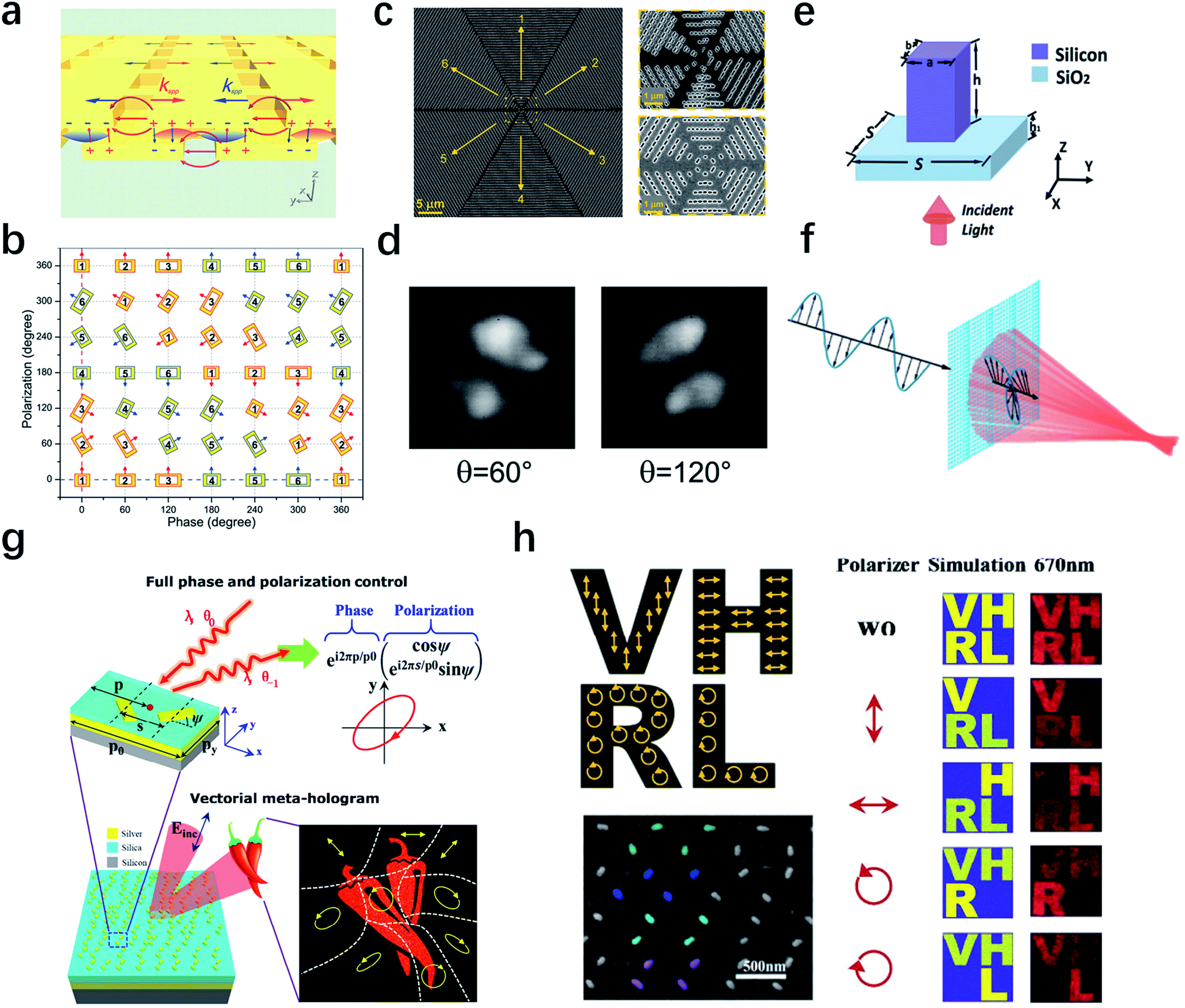 | ||
| Fig. 4 Metasurfaces for simultaneous control of phase and polarization. (a) Schematic of the dual-layer plasmonic metasurfaces composed of rectangular nano-apertures. (b) The diagram for the full control of polarization and phase, in which 36 pairs of nano-apertures with different parameters are used. (c) SEM image and (d) measured far-field intensity profiles of the plasmonic metasurfaces to generate a radially polarized beam. (e) Schematic of the unit cell for dielectric metasurfaces. (f) Sketch map of a focusing lens combined with a quarter-waveplate. (g) Illustration of the unit cell of a meta-hologram to generate a holographic image with spatially varying polarization states. Three parameters, including local displacement s, global displacement p and orientation angle ψ of two orthogonal Au nanorods can be used to simultaneously control the phase and polarization. (h) Experimental demonstration of vectorial holography. Four sets of diatomic meta-molecules are arranged in sequence, then each letter in holographic image represents one single specific polarization. (a–d) Reproduced with permission.104 (e and f) Reproduced with permission.107 (g and h) Reproduced with permission.109 | ||
Apparently, the ideal metasurface is to simultaneously control all the three properties for output light, including phase, polarization and amplitude. A single metasurface with such a capability can realize any desired functions in a deep subwavelength thickness, promising revolutionary advances in the fields of integrated photonics. The first demonstration for this attempt was reported by Lin et al. in 2013.110 The authors designed a new type of holographic interface that can manipulate the phase, amplitude, and polarization, over a broad wavelength range (Fig. 5a). The phase control utilizes the concept of detour phase, which originates from the diffraction angle and forms a linear phase ramp. Then the aperture position along the x-axis within each pixel locally controls the phase of the transmitted light. The amount of light passing through the pixel is proportional to the length of the aperture, which can be used to modulate the amplitude. And lastly, polarization modulation can be realized by rotating the orientation angle of the aperture. Using this design, the authors have demonstrated a metasurface to create a radially polarized beam. The experimentally fabricated sample is shown in Fig. 5b, which integrates subwavelength apertures for polarization control and wavelength-scale diffracting apertures for phase and amplitude modulation. The desired hollow intensity distribution of a typical radially polarized beam is shown in the right panel of Fig. 5b, in which blue arrows indicate the directions of polarization. The measured far-field intensity distributions in Fig. 5c clearly show that the m = +1 beam is radially polarized. In addition to the holographic pattern, the scattering fields and reconstruction of the polarization, amplitude, and phase of the transmitted light are also important in transformation optics,111 especially for an invisibility cloak.112–114 Previously reported invisibility cloaks were limited on special polarizations113 or encountered amplitude/phase distortions.112 A 3D full-polarization clock with the ability to well control all three properties of scattering light was demonstrated using metasurfaces (Fig. 5d), in order to have the same phase compensation for any polarization, a closed ring resonator with four-fold rotation symmetry was introduced as the unit cell of the metasurface. The simulation result in Fig. 5e shows that, when the incident angle changes from 0° to 45°, the phase profiles for TE and TM polarization with different sizes of ring resonators are very similar and can cover the 2π range while the intensities remain constant. The measured field distributions of different planes in Fig. 5f demonstrate good cloaking performance for such an invisibility cloak, confirming the effectiveness of simultaneous control of three properties of output light.
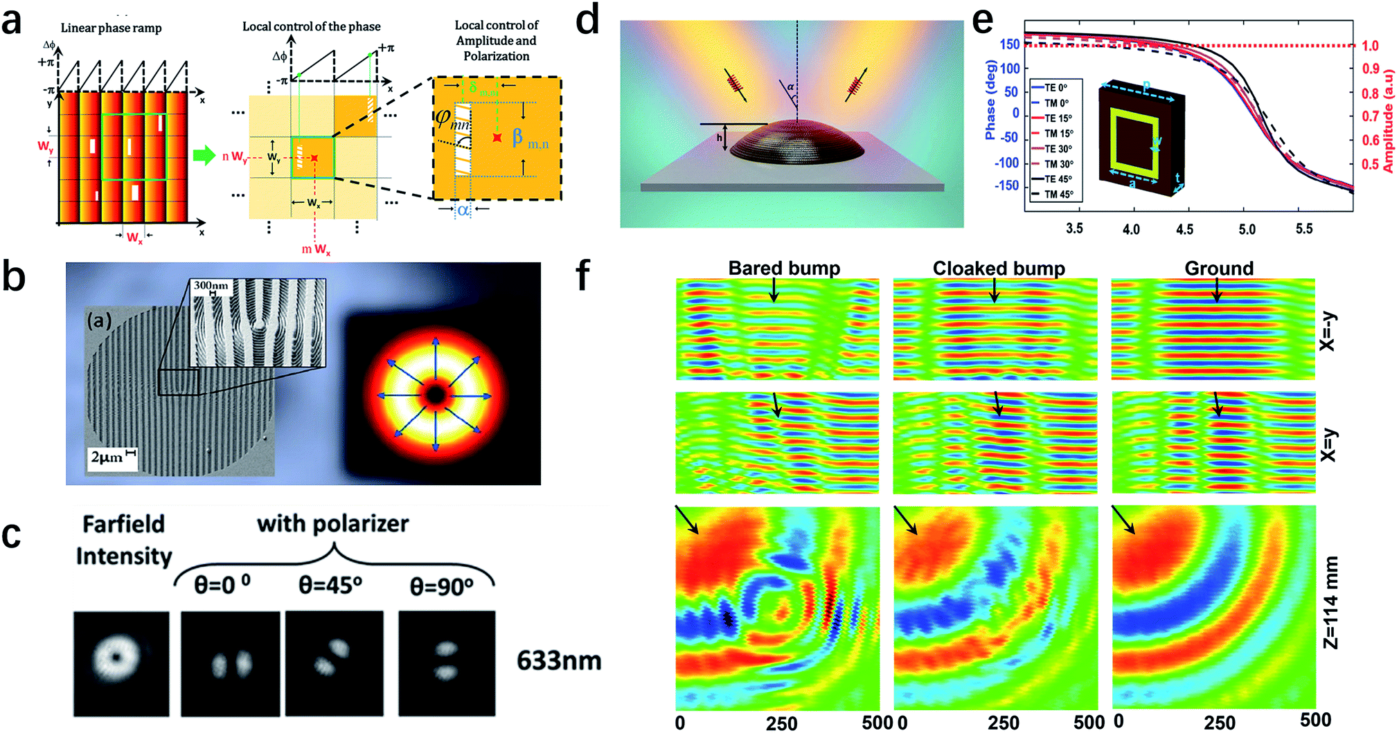 | ||
| Fig. 5 Metasurfaces for the full control of the phase, amplitude and polarization of light. (a) Schematic of the nanostructure to simultaneously control the three properties of output light. The position and size of the slit are introduced to control the phase and amplitude, while the orientation angle determines the polarization state. (b) SEM image and (c) measured far-field intensity distributions of a holographic plate to generate radially polarized beams, which combines a radial polarizer and a fork diffraction hologram. (d) Schematic of the metasurfaces carpet cloak that can preserve the amplitude, phase, and polarization of the reflected light. (e) Simulated phase (dashed lines for TM and solid lines for TE) and amplitude (dotted lines) for unit cells with different parameters and incident angles. (f) The measured field in the x = −y, x = y and z plane for a bare bump, cloaked bump, and flat mirror, respectively. The black arrows represent the incidence direction of the electromagnetic wave. (a–c) Reproduced with permission.110 (d–f) Reproduced with permission.115 | ||
4. Controlling the input wavelengths to realize dispersion control
In the next chapters, including Section 4–6, we will mainly focus on the input DOF for metasurfaces. First of all, we would like to discuss the wavelength, because it is relevant to multispectral achromatic optics.34,116,117 In most cases, resonant nanostructures have limitations in spectral responses, thus hindering multi-wavelength or broadband applications. One straightforward method to realize multi-wavelength devices is to combine different plasmonic nanostructures that work at different wavelengths.117–121 Using this design, Huang et al. reported a multicolor meta-hologram that is able to produce images in three primary colors as Fig. 6a shows.119 The unit cell is composed of aluminum nanorods that support surface plasmon resonances for red (R), green (G), and blue (B) light. Under linearly polarized illumination, three images, that is, R, G and B, can be clearly observed in the hologram plane. To further increase the effective efficiency, dielectric metasurfaces can be used alternatively. In 2016, Li's group showed a silicon metasurface in the visible as shown in Fig. 6b, enabling wavefront manipulation for R, G, and B light simultaneously.121 The strong confinement of the fields inside these Si nanoblocks substantially suppresses their interactions between each nanoblock, so that the phase for each color can be manipulated independently. A highly dispersive metahologram projects distinct images: a flower, a peduncle and a pot, respectively, at R, G, and B wavelengths. The efficiency is around 50%, one order of magnitude higher than those of plasmonic color holograms demonstrated before.119 Besides integrating different nanoparticles on a single plane, multilayers metasurfaces can also be designed to work for different wavelengths. As Fig. 6c shows, Avayu et al.116 introduced a scheme of cascading three layers of metasurfaces, where each layer is optimally designed for a specific color. Using this approach, the authors demonstrated an achromatic metalens operating at R, G and B wavelengths. All these demonstrations open a new door to ultra-thin achromatic optical elements with multiple functionalities.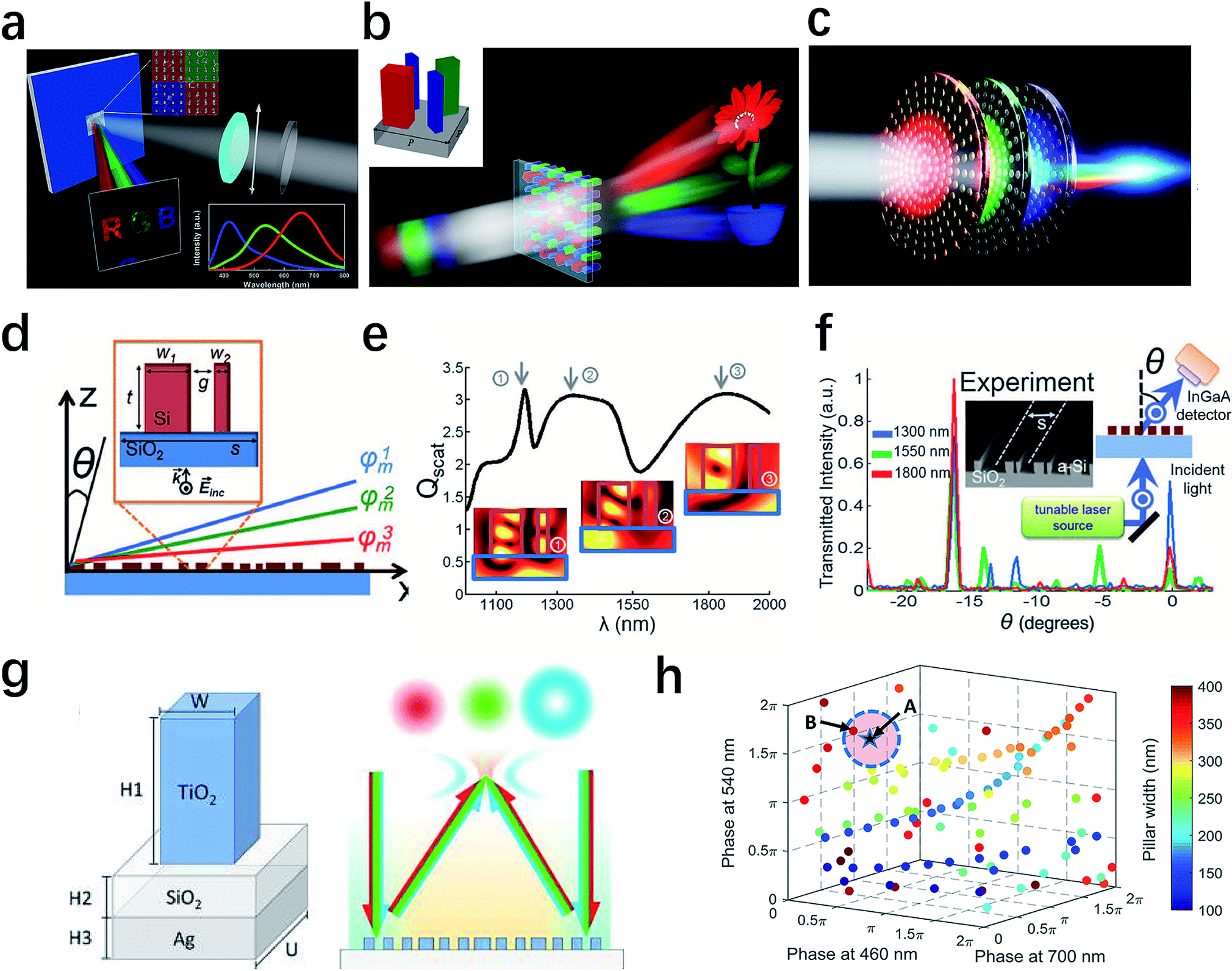 | ||
| Fig. 6 Metasurfaces for dispersion control at discrete wavelengths. (a) Illustration of the designed multicolor meta-hologram composed of three kinds of aluminum nanorods, each of which controls one wavelength. As a result, images of letter R, G, and B can be generated. (b) Schematic of the dispersive hologram realized by dielectric metasurfaces. The unit cell consists of three different kinds of Si nanoblocks. (c) Schematic of the three-layer metasurfaces lens. Each layer focuses different designed wavelength to the same distance to realize an achromatic metalens. (d) Schematic of a multiwavelength achromatic metasurface to diffract normally incident plane waves at three discrete wavelengths to the same angle θ with respect to z-axis. Each unit cell contains two coupled rectangular Si resonators. (e) Scattering efficiency for one unit cell, which supports three resonances at the target wavelengths. (f) Measured diffraction angles at 1300, 1550 and 1800 nm, which are nearly the same. (g) Schematic of the unit cell (left panel) and the metasurfaces with controllable multiwavelength functions, which can generate different orbital angular momentum at different wavelengths (right panel). (h) The simulated phases at 460, 540 and 700 nm for TiO2 pillars with different width. The black star A indicates the required ideal phase point and red point B means the nearest neighbor of A among those that can be realized in experiments. (a) Reproduced with permission.119 (b) Reproduced with permission.121 (c) Reproduced with permission.116 (d–f) Reproduced with permission.34 (g and h) Reproduced with permission.123 | ||
Another interesting method to control the phase for different wavelengths is to engineer the dispersion.34,35,122,123 It is known that material dispersion, meaning the refractive index varies with the frequency, often limits the practical applications of optical lenses because of chromatic aberration. Moreover, the phase difference through light propagation in free space with various wavelengths can also generate large dispersion. However, these two limitations can be addressed by an engineered wavelength-dependent phase shift via a metasurface.34Fig. 6d depicts the side view of a unit cell that comprises two coupled rectangular dielectric resonators. The scattering spectrum in Fig. 6e demonstrates that the low-loss dielectric resonators can introduce multiple optical modes to enable dispersive phase compensation. Using this strategy, a sample that deflects three wavelengths, including 1300, 1550 and 1800 nm, by the same angle has been successfully demonstrated in experiments (Fig. 6f). Apart from realizing the achromatic phase, which can also be regarded as zero-dispersion,35 interesting phenomena like hyper-negative dispersion can be realized by this approach.35 More recently, using the similar design principle, Capasso's group reported dispersion-engineered metasurfaces with distinct functionalities controlled by wavelengths,123 which open a path to applications such as compact multiwavelength beam generation. As schematically shown in the left panel of Fig. 6g, the unit cell consists of a titanium dioxide nanopillar, a thin silicon dioxide spacing layer and a silver substrate. In this design, sharp resonances can effectively decouple the realized phases at different wavelengths by properly tuning the geometric parameters, so that independent control of metasurfaces functions, such as the wavelength-multiplexed orbital angular momentums generation illustrated in the right panel of Fig. 6g, can be achieved at discrete wavelengths. Fig. 6h shows the simulated results in phase space at 460, 540 and 700 nm, respectively, in which each circular point corresponds to a specific designed nanopillar and color map represents the pillar width. In principle, we can expand the number of operating wavelengths to accommodate integration of more complex functionalities.
Up to now, we have focused on the wavelength control at several discrete values. None of them realizes the continuous broadband dispersion management.36,124 However, for applications like metalenses, the achromatic performance is required over a wide wavelength range, because usually the illumination source or the signal covers a substantial bandwidth. One breakthrough of an achromatic metalens (AML) was demonstrated by Khorasaninejad et al. in 2017.124 As illustrated in Fig. 7a, the AML comprises titanium dioxide nanopillars on a substrate, which can be fabricated by a one-step lithography process. Fig. 7b plots the simulated and experimental results of the focal length of the AML as a function of wavelength, which shows a constant focal length across an entire wavelength range from 490 to 550 nm. These results unambiguously demonstrate the achromatic behavior of the AML in the visible range and manifest opportunities for the development of novel optical components with dispersionless performances. Soon after, Wang et al. proposed a design principle to realize achromatic meta-devices that can eliminate the chromatic aberration over a continuous wavelength for circularly-polarized light in a reflection scheme.36 From the SEM image of the fabricated metalens presented in Fig. 7c, one can see that a set of integrated-resonant unit elements are arranged in a ring form. These elements are designed with linear and smooth phase dispersion combining with geometric phase, which can provide the phase compensation between different wavelengths. This approach enables the phase compensation up to 2π and a fairly high efficiency at most wavelengths. The performance of the achromatic converging metalens has been systematically investigated over a broad infrared bandwidth ranging from 1200 to 1680 nm (Fig. 7d). The broadband achromatic meta-devices based on this approach may accelerate a complete class of designs for full-color light manipulation.
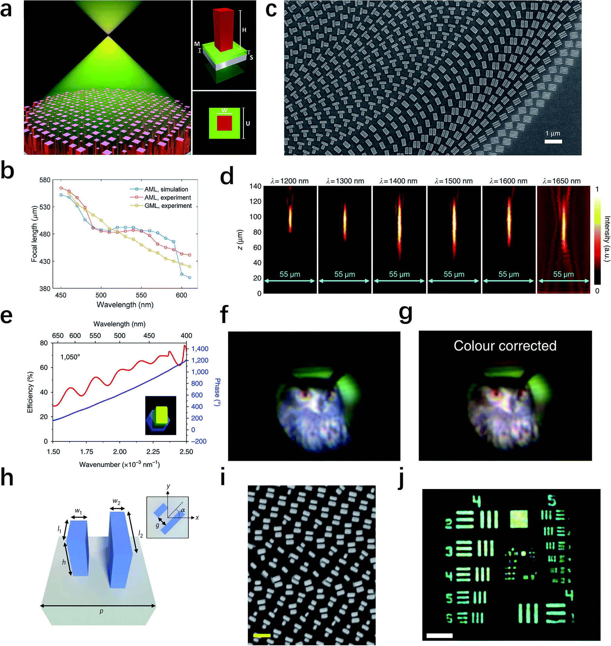 | ||
| Fig. 7 Metasurfaces for broadband dispersion control. (a) Schematic of an achromatic metalens that consists of titanium dioxide nanopillars. (b) The calculated and measured results of achromatic metalens demonstrate the focal length nearly remains the same from 490 to 550 nm. (c) SEM image of the broadband achromatic metalens in reflection configuration, where the integrated-resonant unit elements are employed. (d) Measured intensity profiles of the reflected beam along the axial planes at different wavelengths, showing negligible variation of focal length. (e) Calculated polarized conversion efficiency (red curves) and phase profile (blue curve) for an integrated resonant unit element, which is shown in the inset. (f and g) Full-color Eurasian eagle owl images formed by the achromatic metalens before and after color correction. (h) Unit cell design for broadband achromatic metalens in transmission configuration, which is composed of one or two TiO2 nanofins with different geometric parameters. (i) SEM image of the fabricated sample for the design in (h). Scale bar: 500 nm. (j) Achromatic imaging by the fabricated metalens under a white light (470–670 nm) illumination. Scale bar: 200 μm. (a and b) Reproduced with permission.124 (c and d) Reproduced with permission.36 (e–g) Reproduced with permission.125 (h–j) Reproduced with permission.126 | ||
For practical applications, transmission-type components are more useful and convenient than reflective ones. Two important papers have been independently published almost at the same time for this reason.125,126 One of them used gallium nitride to construct unit elements to support waveguide-like resonant modes in the visible regime.125 Resonant unit elements were implemented as the building blocks in order to introduce integrated resonances for required phase compensation.36 The simulated phase and amplitude response are plotted in Fig. 7e, demonstrating that the phase compensation reaches 1050°. The focal length of the metalens remains unchanged as the incident wavelength varies from 400 to 660 nm, indicating that the chromatic aberration is eliminated across about 49% bandwidth with respect to the central working wavelength. Remarkably, the average efficiency of the metalens with a numerical aperture of 0.106 is about 40% over the entire visible spectrum. Finally, the authors showed full-color imaging using the achromatic metalens (Fig. 7f and g), demonstrating that their design has great potential for full-color optical techniques and applications. In the other work, TiO2 nanostructures as shown in Fig. 7h and i were introduced to engineer the frequency dependent phase profile,126 which can achieve appropriate control of dispersion over a large continuous bandwidth in the visible. The authors demonstrated diffraction-limited achromatic focusing and achromatic imaging from 470 to 670 nm in Fig. 7j. With the well-developed design principles, more requirements can be incorporated into achromatic metalenses, such as polarization independence, as demonstrated by recent works in the near-infrared and visible region.127,128 All these exciting works are expected to impact both industry and scientific research in the areas of microscopy, lithography, endoscopy and virtual and augmented reality.
5. Controlling the input polarization to realize polarization multiplexing
The second input DOF we want to discuss is the polarization. A polarization-dependent focusing lens operating at far-infrared wavelengths was demonstrated by Hasman et al. in 2003,129 while it was not coined metalens. Then the concept of dual polarity was introduced by Chen et al.130 into metasurfaces in 2012. Instead of only considering one input polarization as in previous works,1,15 the authors controlled both RCP and LCP light, realizing a dual-polarity tunable plasmonic metalens for visible light. This work and others show tremendous potential in helicity-dependent focusing, sensing and imaging devices,27,32,131–133 angular-momentum-based quantum information processing134–136 and directional coupling of surface plasmon polaritons.30,137,138 Another work (Fig. 8a) adopted a thinning technique to investigate interleaved sparse nanoantenna matrices.136 With the spin-enabled asymmetric harmonic response, such a metasurface is able to achieve helicity-controlled multiple structured wavefronts, including vortex beams carrying orbital angular momentum. For traditional segmentation methods, in which the aperture is spatially divided into separated subarrays imprinted with different phase functions, the reduction of angular resolution is inevitable. While for the interleaved approach, in which multiple desired phase profiles are interleaved within the entire aperture, the simulated results demonstrate significantly enhanced angular resolution. This thinning procedure can be implemented using combinatorial algorithm and fractal arrangement to achieve sufficient bandwidth, and desired functionality. The shared-aperture metasurface platform introduces multiple DOF and opens a pathway to innovative nanophotonic devices and systems.139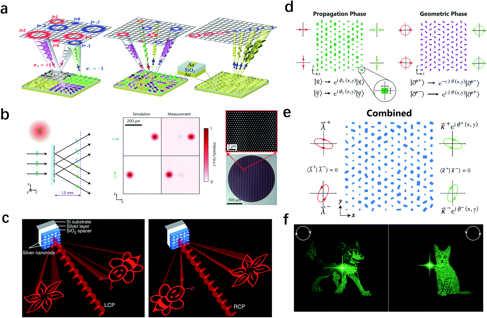 | ||
| Fig. 8 Metasurfaces for polarization multiplexing. (a) Generation of multiple orbital angular momentum states from segmented (left), interleaved (middle) and harmonic response (right) metasurfaces that consist of gap-plasmon nanoantennas (inset). (b) Illustration (left), intensity profiles (middle), optical performances and SEM image (right) of a polarization beam splitter, which deflects orthogonal linear polarized light by different angles. (c) Schematics of the helicity multiplexed metasurface hologram. Under the illumination of LCP and RCP light, different holographic images will be constructed. (d) Independent phase control of two orthogonal linear (left) and circular (right) input polarizations by propagation phase (left) and geometric phase (right), respectively. (e) By combining the geometric and propagation phases, which means controlling both dimensions and orientation angles of elements, independent phase control of arbitrary orthogonal states of polarization can be realized. (f) Experimental demonstration of two independent holographic images with one single metasurface. A cartoon dog (cat) will emerge under RCP (LCP) illumination. (a) Reproduced with permission.136 (b) Reproduced with permission.31 (c) Reproduced with permission.32 (d–f) Reproduced with permission.142 | ||
Polarization-multiplexed holograms for linearly polarized light was proposed in the reflected plasmonic system at the very beginning,27 while soon extended to transmissive dielectric metasurfaces.31 As shown in Fig. 8b, a metasurface consists of high-contrast dielectric nanoposts could function as a polarization beam splitter. The nanopost, which can be regarded as a waveguide with an elliptical cross-section, has different phase responses for x- and y-polarization owing to the different effective refractive indices along the two ellipse axes. The experimental results clearly show that this beam splitter could deflect x- and y-polarized light to different directions, with an efficiency ranging from 72% to 90%. The idea of utilizing the polarization of incident light as another DOF provides opportunities to achieve multi-dimensional/multi-functional metasurfaces and can be further extended to other polarizations like circularly polarized light.32,131,140,141 As shown in Fig. 8c, a broadband helicity multiplexed metasurface, which consists of two sets of unit cell working at two orthogonal helicities independently, shows the holographic images “flower” at the left side and “bee” at the right side for LCP incident light. When the incident light is switched to RCP, the two images are swapped in position. The conversion efficiency remains higher than 40% from 620 nm to 1020 nm. In order to achieve a polarization multiplexed hologram for arbitrary orthogonal polarization states,139 a metasurface composed of silicon nanoblocks with different geometric sizes and orientation angles was reported.142 In this structure, the propagation phase, which is determined by the dimensions of silicon nanoblocks, and the geometric phase, which is determined by the rotation angle, were combined to achieve arbitrary phase profiles for any set of orthogonal polarization states (Fig. 8d and e). The holograms display “dog” and “cat” images for RCP and LCP illumination, respectively, as shown in Fig. 8f. This approach further extends the polarization from linear to any polarization state, which could significantly broaden the scope of polarization-sensitive hologram devices.
6. Controlling the incident angle to realize angle multiplexing
In practical applications, very often we require that optical devices have tolerance to the angle of incidence.143 Such a requirement has motivated researchers to investigate metasurfaces with strong angle insensitivity. This is particularly important for perfect absorbers,144–146 planar metalenses,147 and hologram displays.148 Conventional metasurfaces and most diffractive devices have a similar angular characteristic, because of the weak angular sensitivity of the meta-atoms. However, this fundamental property can be altered by a special design,149,150 which is called angle-multiplexed metasurfaces introduced by Kamali et al. in 2017.149 The unit cell in their design is composed of high-index U-shaped meta-atoms as shown in Fig. 9a, whose responses subjected to incidence from different angles can be controlled independently. The underlying mechanism is the excitation of different resonant modes at the incident angle of 0° and 30°, which is indicated by the distinct field distributions depicted in Fig. 9b. Since the different resonant modes at the two angles are directly related to the geometric parameters of the meta-atoms, a properly designed meta-atom is capable of generating two arbitrary phase profiles independently, implying that the incident angle could be regarded as another degree of freedom. In this work, the holographic images of Caltech and LMI were created at the incident angle of 0° and 30°, respectively. As shown in Fig. 9c, the experimental results agree well with the simulation results. Cascaded multilayer metasurfaces, with each layer performing a predefined mathematical transformation, can also realize the similar function.150Fig. 9d is the schematic illustration of the cascaded metasurfaces, in which two metasurfaces are patterned on the opposite sides of a glass substrate. The entire device is designed as a retroreflector to reflect light along the opposite direction of the incident beam over a broad range of incident angles. Such a function is rather challenging, because angular correlation exists in diffractive devices and traditional metasurfaces. Here, when light with different incident angles passes through metasurface I, which was designed as a converging lens, it would be directed to a different location on metasurface II. Then the light would be reflected back along the incident route because of the additional spatial varying momentum imparted by the phase gradient in metasurface II. Using this method, a retroreflector consisted of two metasurfaces was fabricated and measured as shown in Fig. 9e. The experimental results in Fig. 9f show good quality of the reflected images with the retroreflector rotating up to 20°, demonstrating that its effective working range can reach 40°. The angle-multiplexed capabilities are complementary to the previously reported broadband achromatic response and polarization-multiplexed effect, and hence could further expand the functionalities and applications of metasurfaces.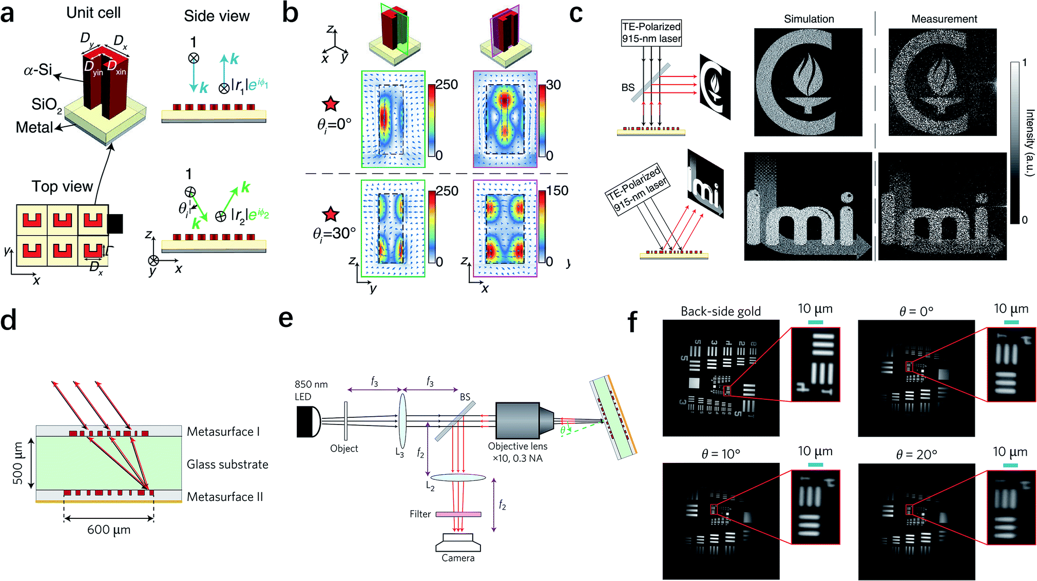 | ||
| Fig. 9 Metasurfaces for incident angle multiplexing. (a) Schematic drawing of the unit cell of angle-multiplexed metasurfaces. A U-shaped Silicon meta-atom is introduced as a multimode resonator. (b) Simulated electric field distribution in two cross sections under the illumination angels of 0° and 30°. Different resonant modes are excited to provide independent phase control of two incident angles. (c) Experimental setups (left) and simulated and measured holographic images (right) illuminated at 0° and 30° angles. Two different images (Caltech and LMI logos) demonstrate that independent phase can be realized under different incident angles. (d) Schematic drawing of a planar retroreflector, which is composed of two metasurfaces separated by a 500 μm glass substrate. With the spatial Fourier transformation of metasurface I and momentum compensation of metasurface II, light can be reflected back to the direction opposite to the incidence. (e) Illustration of the measurement set-up. (f) Measured images of a resolution target onto the retroreflector with various rotation angles. (a–c) Reproduced with permission.149 (d–f) Reproduced with permission.150 | ||
7. Dynamic control of the metasurfaces
In previous sections, we have discussed the inherent DOF of light waves, which can be used for realizing various metasurfaces with extraordinary advantages. Nevertheless, most of the metasurfaces are static, meaning their functions are fixed once the metasurfaces are fabricated. It is of great interest and importance to realize dynamically tunable or reconfigurable metasurfaces via outer conditions as shown in Fig. 1, including external fields,155–158 mechanical deformation,159–161 and phase change materials.162–165 For example, vanadium dioxide (VO2), a thermal-sensitive phase change material, has been demonstrated successfully for beam scanning166 or polarization switching.167 On the other hand, applying electric fields is arguably the most direct and preferred method to realize dynamic control in liquid crystals,168 graphene,89,155,169–172 and ITO.173 Electrical reprogrammable holograms have been demonstrated in microwave frequencies by integrating electric diodes into the unit cells of metasurfaces.151 As shown in Fig. 10a, by controlling the DC bias voltage applied on each diode, the reflection coefficient of the output electromagnetic waves from the metasurface can be tuned. In order to achieve a dynamic tuning of the hologram, a field programmable gate array was used to control the phase shift for each single unit. Three different holographic images “P”, “K” and “U” are generated using this method. Although this metasurface work at microwave frequencies, in principle it could be extended to higher frequencies like terahertz, which may find its further applications in security, data storage and information processing.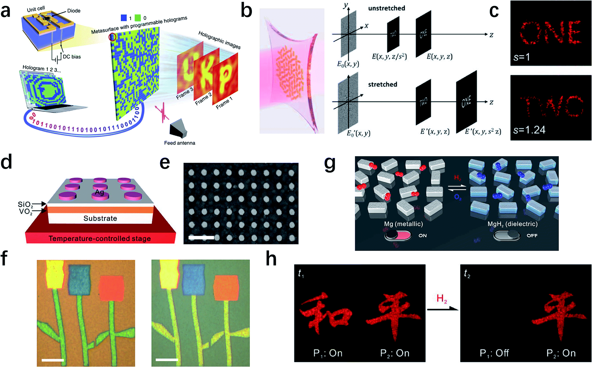 | ||
| Fig. 10 Dynamic metasurfaces based on external fields, mechanical deformation and phase change materials. (a) Schematic of the reprogrammable coding metasurfaces hologram. By applying DC voltages across the positive-intrinsic-negative diode, the reflection coefficient can be controlled and reprogrammable holographic images can be realized. (b) Illustration of a strain-multiplexed metasurface hologram. As the substrate is stretched, the two-plane hologram image moves away from the device. If the detection plane is fixed, the switch of holographic image can be observed. (c) Experimentally measured image switching from “ONE” to “TWO”. (d) Illustration and (e) SEM image of the dynamic plasmonic color generation based on VO2. Scale bar: 600 nm. (f) Measured reflection images of the flower pattern at 20 °C (left) and at 80 °C (right), demonstrating the changing of multiple plasmonic colors. Scale bar: 40 μm. (g) Schematic of dynamic metasurfaces holograms using chemical reactions. The hydrogen-responsive Mg nanorods undergo a phase transition from metal to dielectric (MgH2) upon hydrogen loading. (h) Measured holographic images during hydrogenation and dehydrogenation. By switching the input state from On to Off, the left holographic pattern (harmony) diminishes while the right holographic pattern (peace) remains. (a) Reproduced with permission.151 (b and c) Reproduced with permission.152 (d–f) Reproduced with permission.153 (g and h) Reproduced with permission.154 | ||
Another effective outer control is mechanical deformation. In most cases, this strategy is realized by embedding plasmonic nanoantennas or dielectric resonators in an elastic substrate, such as elastomeric matrix,159 stretchable polydimethylsiloxane160 and transparent elastic polymer.161 However, these devices only focus on the simple active effect such as spectrum shift and tunable metasurfaces lenses. In 2017, Malek et al. demonstrated reconfigurable phase-only computer generated metasurfaces holograms fabricated with gold nanorods on a stretchable polydimethylsiloxane substrate, which can show two image planes operating in the visible regime (Fig. 10b).152 Using computational techniques for generating multiplane holograms, the authors designed a two-plane metasurfaces holograms. As the metasurface is stretched, all image planes will move away from the metasurfaces. If the detection plane remains unchanged upon stretching, the observed hologram image changes between different pictures (Fig. 10c). It shows the possibility to realize the reconfigurable devices by metasurfaces designed on a stretchable substrate.
Besides the two methods we have mentioned above, phase change materials provide a very nice platform to realize dynamic control, in which external field can change the effective refractive index and affect the optical response of the metasurfaces. Apart from the perfect absorber,155 reflected phase change,158,163 dynamic plasmonic color display165 is another interesting topic emerged in recent years. In Fig. 10d and e, the periodic array of silver nanodisks are integrated with phase change material VO2 to achieve dynamic color generation. Because of the insulator-metal transition of VO2 upon the temperature change, the colors arising from localized surface plasmons can be tuned by controlling the temperature. To further demonstrate this strategy, reflection images of a well-designed “flower” pattern at 20 °C (left) and at 80 °C (right) are captured (Fig. 10f), indicating the potential possibilities in a dynamic colorful display system. Moreover, reconfigurable holograms have also been demonstrated via phase change materials.154,174 Moving forward, Liu's group reported chemically active metasurfaces (Fig. 10g) by utilizing the unique hydrogenation and dehydrogenation characteristics of magnesium (Mg).154 It can undergo a phase transition from metal to dielectric upon hydrogen loading, forming magnesium hydride (MgH2), while the transition is reversible through dehydrogenation upon oxygen loading, returning to Mg. Consequently, we can repeatably turn on and off the plasmonic response of Mg nanorods in the metasurface and realize a dynamic plasmonic pixel. Using this property, dynamic metasurfaces holograms at visible frequencies have been implemented (Fig. 10h). By switching the input state of sample P1 from “On” to “Off”, the corresponding holographic pattern of “harmony” diminishes, whereas the pattern of “peace” remains unchanged, verifying the dynamic control of holographic images.
8. Sophisticated designs for multiple degrees of freedom
In this section, we will discuss several sophisticated metasurface examples published recently, which consider multiple input and output DOF to demonstrate more intriguing phenomena. For the first example shown in Fig. 11a, the input DOF changes from single-wavelength coherent light to white light and the output DOF also changes from phase to amplitude, producing the holographic image of “3.141592…”and the reflective colored image of “π”, accordingly. Thus, the concept of dual-mode metasurfaces was realized.175 In the design, when single-wavelength light irradiates on the metasurface, additional phase distribution would be endowed to the transmission light to generate a hologram image, which refers to the transmission mode. Meanwhile, a reflective colored image is produced under white light illumination, which represents the reflection mode. The unit cell has two parallel identical nanoantennas as shown in Fig. 11b. The simulated cross-polarization transmittance (CPT) spectra shown in Fig. 11c indicate that for two different parameters, the CPT has almost the same value at the target wavelength of 635 nm but different spectrum shapes in the visible range. This means such two parameters can realize the same PB phase response while exhibiting different reflected colors. Using this dual-mode metasurface, the authors designed a crypto-display system in the experiment as the schematic shown in Fig. 11a. The optical image of the sample seems to be a normal letter of “π” under white light illumination, but it will generate an encrypted holographic image under coherent light illumination. Considering those two modes are independent of each other, this work can be potentially applied in the security technique.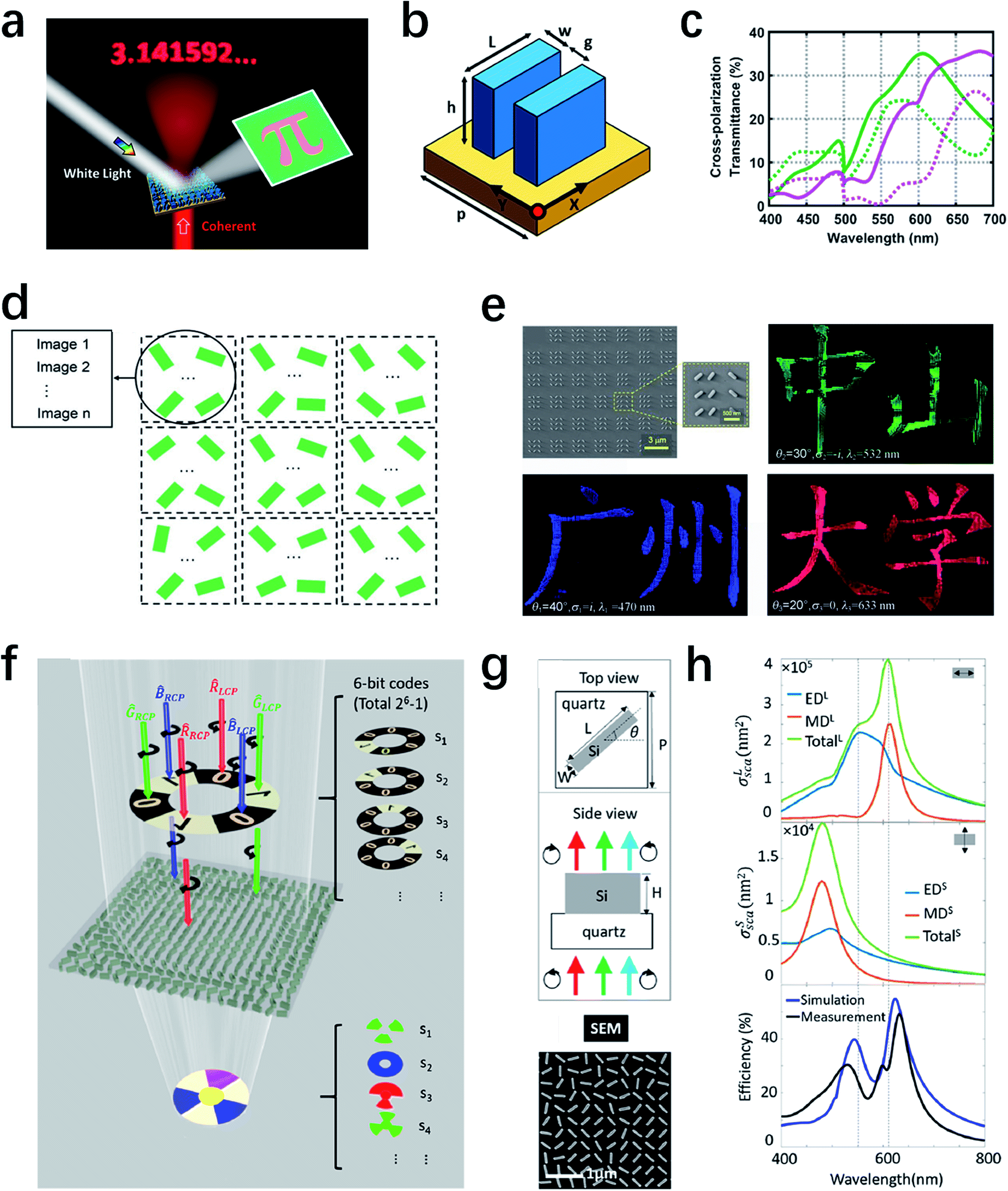 | ||
| Fig. 11 Combination of multiple input DOF and output DOF. (a) Schematic of the crypto-display in a dual-mode metasurface. The transmission mode produces one holographic image with the incidence of coherent light, whereas the reflection mode represents an independent colored image with the incidence of white light. (b) Illustration of the unit cell which comprises two parallel identical Si nanoantennas. (c) Calculated cross-polarization transmittance of two different nanoantenna designs represented by red and blue curves. Solid lines: the parallel double nanoantennas. Dotted lines: the single nanoantenna. (d) Schematic of the coherent pixel, composed of multiple identical elements that contribute together to different images. (e) SEM and optical images of the fabricated samples. Under three incident conditions, different images with Chinese words of “Guang Zhou”, “Zhong Shan,” and “University” can be clearly observed, respectively. (f) Schematic of the spin and wavelength encoded holograms. By controlling six fundamental bases of the input beams, multiple colorful images can be reconstructed and transfer the encoded information. (g) Unit cell design (top) and SEM image (bottom) of a Si metasurface to realize wavelength- and spin-dependent images. The simulated and measured results in (h) demonstrate that three modes exist in the silicon nanobrick, working for three target wavelengths. (a–c) Reproduced with permission.175 (d and e) Reproduced with permission.176 (f–h) Reproduced with permission.177 | ||
The second example shown in Fig. 11d considers the incident angle, wavelength, and polarization as the input DOF while the amplitude of the printing image is considered for the output responses.176 In order to achieve multiple printing-image switching controlled by arbitrary input optical parameters, a novel method called “coherent pixel” is introduced in this work. Different from the previous design of multiplexed pixel,121 here all the identical elements in one pixel contribute as a whole to the printing images with different input conditions. Using this method, the authors have demonstrated novel functionalities, such as incident-angle controlled and polarization-controlled printing images based on multidimensional control under different illumination conditions. As shown in Fig. 11e, the measured images clearly show Chinese words of “Guang Zhou”, “Zhong Shan” and “University” with different incident parameters, respectively. Moreover, the authors claim that this method can be further extended for more image switching by increasing the number of elements in one pixel. This method is promising for various applications, including multi-functional flat devices and optical encryption.
As for the last example illustrated in Fig. 11f, the input DOF is wavelength and polarization, while the output DOF is phase.177 As we have mentioned above, in order to achieve multi-functional metasurfaces, extra spatial DOF has been introduced, including interleaved subarrays136 and different angles.149 However, in this work, the 6 bit encoded color holograms were achieved by noninterleaved single-size Si nanobrick and minimalist spatial freedom. As shown in Fig. 11g and h, three modes at red, green and blue wavelengths can be supported in the Si nanobricks with appropriate parameters. In this dielectric nanostructure with different rotation angles, 6 bit images which are related to the wavelengths and polarizations can be generated by the interference of the electric dipole and magnetic dipole under six bases of the incident light. Each of the basis corresponds to one monochromatic light with one polarization. Consequently, by combining the six bases in a certain sequence, holographic images with the amount up to 63 could be generated.
9. Conclusions and outlook
Metasurfaces provide unprecedented opportunities to achieve novel capabilities on a platform with deep subwavelength thickness. In this review, we have used the concept of DOF to understand and analyze multi-dimensional functionalities of metasurfaces. At the early stages of development, metasurfaces mainly focused on light manipulation in one dimension like phase, amplitude and polarization, which could be regarded as transferring one input DOF to one output DOF. We have summarized several methods to efficiently control the single property of propagating light owing to the interaction between designer structures and light, which realize desired performances in applications, such as holograms, polarization converters and perfect absorbers. Furthermore, simultaneous control of multiple output DOF has also been discussed. These designs, including phase with amplitude, phase with polarization and even all of the three properties, can greatly improve the performances of metasurfaces for output light and realize some novel phenomena, such as the generation of arbitrary diffraction patterns and arbitrary vectorial holographic images. To achieve such complex modulation, more than one geometric parameter should be considered in the design of unit cells, like both the size and orientation angle of nanoantennas. In addition, various input DOF can be utilized to design multi-functional meta-devices that are also called multiplexed metasurfaces. For different illumination conditions, including working wavelengths, polarization states and angles of incidence, different resonant modes can be excited to modulate the phase of output light independently, enabling us to realize the full-color holograms, spin-controlled wavefront shaping and planar metasurfaces retroreflectors. Bias voltage control, phase change materials and mechanical deformation are the other kinds of input DOF, introducing more variables to the system and generating dynamic metasurfaces. Then by combining multiple input and output DOF together, the application domain of multi-dimensional metasurfaces could be dramatically extended, which makes it very promising for the next generation of multi-functional and compact optics.Because of the progressively increased complexity of multi-dimensional metasurfaces, so far only a small handful examples have been successfully demonstrated. The most difficult part is how to find the relationship between the design of unit cell with every possible DOF and the desired properties or functionalities. In this case, artificial intelligence, including machine learning and deep learning,178,179 may provide a new and exciting direction in the design and optimization process of complex metasurfaces, especially when the number of DOF becomes very large. The machine learning and deep learning models could search the enormous parameter space in a highly efficient way, as demonstrated recently in the inverse design of nanostructures,180,181 chiral metamaterials,182 topological photonics183,184 and even nanophotonic circuits.185 For instance, in the work for the on-demand design of chiral metamaterials,182 the deep learning model, composed of two bidirectional neural networks, is trained by given examples at the beginning. After that, it can automatically predict the circular dichroism of complicated three-dimensional metamaterials and even retrieve the geometric parameters from the spectral requirements. Compared with the traditional design method based on time-consuming, case-by-case numerical simulations, this data-driven approach shows great advantages in designing complicated meta-systems with high efficiency, generality and fidelity.
Combining all the input and output DOF together, dynamic multi-functional metasurfaces could generate an arbitrary light field under arbitrary illumination conditions, meaning any kind of optical devices can be created in real time. This is arguably the final goal of metasurface development, from the basic research to the practical applications. On the other hand, the dynamic modulation introduces time, a new DOF, to realize an active and even reprogrammable meta-device.186–188 It has been reported that frequency conversion and phase manipulation187 can also be realized within a well-designed time-variant system, but not relying on the change of geometric parameters as in normal space-encoded metasurfaces. However, up to date, most dynamic metasurfaces only focus on the state transition from “On” to “Off”, in which the depth, shape and frequency of time-modulation are all ignored. Very recently, the idea of space-time-coding digital metasurfaces has been proposed188 to realize simultaneous manipulations of electromagnetic waves in both space and frequency domains. However, the dynamic condition is controlled by a bias voltage in positive-intrinsic-negative diodes, which limits the working region to microwave and longer wavelengths. When new dynamic methods are introduced to realize an arbitrary time-modulation in the infrared and visible regime, metasurfaces would impact the display techniques especially for virtual reality and augmented reality.
Finally, more interesting physical systems, such as parity-time symmetry,189–191 Smith–Purcell emission,192–195 2D materials196–198 and topology,199–201 could be introduced as a new DOF. For these research areas, metasurfaces provide an unprecedented opportunity to tailor their inner properties. For example, the polarization state of the Smith–Purcell emission could be well controlled by a metasurface composed of C-apertures,192 which is rather challenging to realize in traditional grating structures. On the other hand, these unique systems also provide new platforms for multi-dimensional metasurfaces to show their versatility. When integrated together, some new topics like polarization-multiplexed parity-time symmetry, voltage-controlled Smith–Purcell emission or dynamic topological photonics could emerge, which would inspire researchers with different backgrounds to explore more exciting possibilities provided by metasurfaces in the future.
Conflicts of interest
There are no conflicts to declare.Acknowledgements
Y. L. acknowledges the supports from the Office of Naval Research (N00014-16-1-2409) and National Science Foundation (ECCS-1916839). R. P. and B. X. acknowledge the supports from the National Key R&D Program of China (2017YFA0303702) and the National Natural Science Foundation of China (Grant No. 11634005).References
- N. Yu, P. Genevet, M. A. Kats, F. Aieta, J.-P. Tetienne, F. Capasso and Z. Gaburro, Science, 2011, 334, 333–337 CrossRef CAS.
- A. V. Kildishev, A. Boltasseva and V. M. Shalaev, Science, 2013, 339, 1232009 CrossRef.
- N. Yu and F. Capasso, Nat. Mater., 2014, 13, 139 CrossRef CAS.
- N. Meinzer, W. L. Barnes and I. R. Hooper, Nat. Photonics, 2014, 8, 889 CrossRef CAS.
- N. M. Estakhri and A. Alù, Phys. Rev. X, 2016, 6, 041008 Search PubMed.
- S. Jahani and Z. Jacob, Nat. Nanotechnol., 2016, 11, 23 CrossRef CAS.
- H.-H. Hsiao, C. H. Chu and D. P. Tsai, Small Methods, 2017, 1, 1600064 CrossRef.
- K. Huang, F. Qin, H. Liu, H. Ye, C. W. Qiu, M. Hong, B. Luk'yanchuk and J. Teng, Adv. Mater., 2018, 30, 1704556 CrossRef.
- L. Huang, S. Zhang and T. Zentgraf, Nanophotonics, 2018, 7, 1169–1190 CAS.
- S. M. Kamali, E. Arbabi, A. Arbabi and A. Faraon, Nanophotonics, 2018, 7, 1041–1068 CAS.
- I. Kim, G. Yoon, J. Jang, P. Genevet, K. T. Nam and J. Rho, ACS Photonics, 2018, 5, 3876–3895 CrossRef CAS.
- B. Liang, J.-C. Cheng and C.-W. Qiu, Nanophotonics, 2018, 7, 1191–1205 Search PubMed.
- X. Wang, Z. Nie, Y. Liang, J. Wang, T. Li and B. Jia, Nanophotonics, 2018, 7, 1533–1556 Search PubMed.
- S. Chen, Z. Li, W. Liu, H. Cheng and J. Tian, Adv. Mater., 2019, 31, 1802458 CrossRef.
- X. Ni, N. K. Emani, A. V. Kildishev, A. Boltasseva and V. M. Shalaev, Science, 2012, 335, 427 CrossRef CAS.
- N. I. Zheludev and Y. S. Kivshar, Nat. Mater., 2012, 11, 917 CrossRef CAS.
- Y. Liu and X. Zhang, Chem. Soc. Rev., 2011, 40, 2494–2507 RSC.
- H.-T. Chen, A. J. Taylor and N. Yu, Rep. Prog. Phys., 2016, 79, 076401 CrossRef.
- M. Khorasaninejad and F. Capasso, Science, 2017, 358, eaam8100 CrossRef.
- F. Monticone and A. Alu, Rep. Prog. Phys., 2017, 80, 036401 CrossRef.
- S. Chen, Z. Li, Y. Zhang, H. Cheng and J. Tian, Adv. Opt. Mater., 2018, 6, 1800104 CrossRef.
- Q. He, S. Sun, S. Xiao and L. Zhou, Adv. Opt. Mater., 2018, 6, 1800415 CrossRef.
- D. Wen, F. Yue, W. Liu, S. Chen and X. Chen, Adv. Opt. Mater., 2018, 6, 1800348 CrossRef.
- M. L. Tseng, H.-H. Hsiao, C. H. Chu, M. K. Chen, G. Sun, A.-Q. Liu and D. P. Tsai, Adv. Opt. Mater., 2018, 6, 1800554 CrossRef.
- D. Neshev and I. Aharonovich, Light: Sci. Appl., 2018, 7, 58 CrossRef.
- X. Luo, Adv. Opt. Mater., 2018, 6, 1701201 CrossRef.
- W. T. Chen, K.-Y. Yang, C.-M. Wang, Y.-W. Huang, G. Sun, I.-D. Chiang, C. Y. Liao, W.-L. Hsu, H. T. Lin and S. Sun, Nano Lett., 2013, 14, 225–230 CrossRef.
- M. A. Kats, R. Blanchard, P. Genevet and F. Capasso, Nat. Mater., 2013, 12, 20 CrossRef CAS.
- G. Zheng, H. Muhlenbernd, M. Kenney, G. Li, T. Zentgraf and S. Zhang, Nat. Nanotechnol., 2015, 10, 308 CrossRef CAS.
- J. Lin, J. B. Mueller, Q. Wang, G. Yuan, N. Antoniou, X.-C. Yuan and F. Capasso, Science, 2013, 340, 331–334 CrossRef CAS.
- A. Arbabi, Y. Horie, M. Bagheri and A. Faraon, Nat. Nanotechnol., 2015, 10, 937 CrossRef CAS.
- D. Wen, F. Yue, G. Li, G. Zheng, K. Chan, S. Chen, M. Chen, K. F. Li, P. W. H. Wong and K. W. Cheah, Nat. Commun., 2015, 6, 8241 CrossRef.
- Z.-H. Wang, Y.-S. Hu, X. Xiong, R.-W. Peng and M. Wang, Opt. Lett., 2017, 42, 1153–1156 CrossRef.
- F. Aieta, M. A. Kats, P. Genevet and F. Capasso, Science, 2015, 347, 1342–1345 CrossRef CAS.
- E. Arbabi, A. Arbabi, S. M. Kamali, Y. Horie and A. Faraon, Optica, 2017, 4, 625–632 CrossRef.
- S. Wang, P. C. Wu, V.-C. Su, Y.-C. Lai, C. H. Chu, J.-W. Chen, S.-H. Lu, J. Chen, B. Xu and C.-H. Kuan, Nat. Commun., 2017, 8, 187 CrossRef.
- N. Yu, F. Aieta, P. Genevet, M. A. Kats, Z. Gaburro and F. Capasso, Nano Lett., 2012, 12, 6328–6333 CrossRef CAS.
- S. Sun, Q. He, S. Xiao, Q. Xu, X. Li and L. Zhou, Nat. Mater., 2012, 11, 426 CrossRef CAS.
- S. Sun, K.-Y. Yang, C.-M. Wang, T.-K. Juan, W. T. Chen, C. Y. Liao, Q. He, S. Xiao, W.-T. Kung and G.-Y. Guo, Nano Lett., 2012, 12, 6223–6229 CrossRef CAS.
- A. Pors, M. G. Nielsen, R. L. Eriksen and S. I. Bozhevolnyi, Nano Lett., 2013, 13, 829–834 CrossRef CAS.
- C. Qu, S. Ma, J. Hao, M. Qiu, X. Li, S. Xiao, Z. Miao, N. Dai, Q. He, S. Sun and L. Zhou, Phys. Rev. Lett., 2015, 115, 235503 CrossRef.
- S. Pancharatnam, in Proceedings of the Indian Academy of Sciences-Section A, Springer, 1956. pp. 398–417 Search PubMed.
- M. V. Berry, J. Mod. Opt., 1987, 34, 1401–1407 CrossRef.
- S.-C. Jiang, X. Xiong, Y.-S. Hu, S.-W. Jiang, Y.-H. Hu, D.-H. Xu, R.-W. Peng and M. Wang, Phys. Rev. B: Condens. Matter Mater. Phys., 2015, 91, 125421 CrossRef.
- Z.-H. Wang, S.-C. Jiang, X. Xiong, R.-W. Peng and M. Wang, Appl. Phys. Lett., 2016, 108, 261107 CrossRef.
- L. Huang, X. Chen, H. Muhlenbernd, G. Li, B. Bai, Q. Tan, G. Jin, T. Zentgraf and S. Zhang, Nano Lett., 2012, 12, 5750–5755 CrossRef CAS.
- M. Kang, J. Chen, X.-L. Wang and H.-T. Wang, J. Opt. Soc. Am. B, 2012, 29, 572–576 CrossRef CAS.
- M. Kang, T. Feng, H.-T. Wang and J. Li, Opt. Express, 2012, 20, 15882–15890 CrossRef.
- D. Lin, P. Fan, E. Hasman and M. L. Brongersma, Science, 2014, 345, 298–302 CrossRef CAS.
- A. Arbabi, Y. Horie, A. J. Ball, M. Bagheri and A. Faraon, Nat. Commun., 2015, 6, 7069 CrossRef CAS.
- M. I. Shalaev, J. Sun, A. Tsukernik, A. Pandey, K. Nikolskiy and N. M. Litchinitser, Nano Lett., 2015, 15, 6261–6266 CrossRef CAS.
- Y. F. Yu, A. Y. Zhu, R. Paniagua-Domunguez, Y. H. Fu, B. Luk'yanchuk and A. I. Kuznetsov, Laser Photonics Rev., 2015, 9, 412–418 CrossRef CAS.
- K. Huang, Z. Dong, S. Mei, L. Zhang, Y. Liu, H. Liu, H. Zhu, J. Teng, B. Luk'yanchuk and J. K. Yang, Laser Photonics Rev., 2016, 10, 500–509 CrossRef CAS.
- M. Khorasaninejad, W. T. Chen, R. C. Devlin, J. Oh, A. Y. Zhu and F. Capasso, Science, 2016, 352, 1190–1194 CrossRef CAS.
- M. Born and E. Wolf, Principles of Optics, Pergamon Press, 1980, vol. 6, pp. 188–189 Search PubMed.
- N. K. Grady, J. E. Heyes, D. R. Chowdhury, Y. Zeng, M. T. Reiten, A. K. Azad, A. J. Taylor, D. A. Dalvit and H.-T. Chen, Science, 2013, 340, 1304–1307 CrossRef CAS.
- L. Cong, W. Cao, X. Zhang, Z. Tian, J. Gu, R. Singh, J. Han and W. Zhang, Appl. Phys. Lett., 2013, 103, 171107 CrossRef.
- R.-H. Fan, Y. Zhou, X.-P. Ren, R.-W. Peng, S.-C. Jiang, D.-H. Xu, X. Xiong, X.-R. Huang and M. Wang, Adv. Mater., 2015, 27, 1201–1206 CrossRef CAS.
- Y. Zhao and A. Alu, Phys. Rev. B: Condens. Matter Mater. Phys., 2011, 84, 205428 CrossRef.
- S.-C. Jiang, X. Xiong, Y.-S. Hu, Y.-H. Hu, G.-B. Ma, R.-W. Peng, C. Sun and M. Wang, Phys. Rev. X, 2014, 4, 021026 Search PubMed.
- F. Ding, Z. Wang, S. He, V. M. Shalaev and A. V. Kildishev, ACS Nano, 2015, 9, 4111–4119 CrossRef CAS.
- Z. Liu, Z. Li, Z. Liu, H. Cheng, W. Liu, C. Tang, C. Gu, J. Li, H.-T. Chen and S. Chen, ACS Photonics, 2017, 4, 2061–2069 CrossRef CAS.
- A. Pors, M. G. Nielsen and S. I. Bozhevolnyi, Opt. Lett., 2013, 38, 513–515 CrossRef.
- J. Soret, Ann. Phys., 1875, 232, 99–113 CrossRef.
- O. Carnal, M. Sigel, T. Sleator, H. Takuma and J. Mlynek, Phys. Rev. Lett., 1991, 67, 3231 CrossRef CAS.
- W. Chao, J. Kim, S. Rekawa, P. Fischer and E. H. Anderson, Opt. Express, 2009, 17, 17669–17677 CrossRef CAS.
- E. Bricchi, J. D. Mills, P. G. Kazansky, B. G. Klappauf and J. J. Baumberg, Opt. Lett., 2002, 27, 2200–2202 CrossRef.
- Y. Ra'di, C. Simovski and S. Tretyakov, Phys. Rev. Appl., 2015, 3, 037001 CrossRef.
- N. Liu, M. Mesch, T. Weiss, M. Hentschel and H. Giessen, Nano Lett., 2010, 10, 2342–2348 CrossRef CAS.
- S. Chen, H. Cheng, H. Yang, J. Li, X. Duan, C. Gu and J. Tian, Appl. Phys. Lett., 2011, 99, 253104 CrossRef.
- H.-T. Chen, Opt. Express, 2012, 20, 7165–7172 CrossRef.
- J. Zhu, Z. Ma, W. Sun, F. Ding, Q. He, L. Zhou and Y. Ma, Appl. Phys. Lett., 2014, 105, 021102 CrossRef.
- Y. Peng, X. Zang, Y. Zhu, C. Shi, L. Chen, B. Cai and S. Zhuang, Opt. Express, 2015, 23, 2032–2039 CrossRef CAS.
- X. Xiong, S.-C. Jiang, Y.-H. Hu, R.-W. Peng and M. Wang, Adv. Mater., 2013, 25, 3994–4000 CrossRef CAS.
- W.-B. Shi, R.-H. Fan, K. Zhang, D.-H. Xu, X. Xiong, R.-W. Peng and M. Wang, J. Appl. Phys., 2015, 117, 065104 CrossRef.
- N. I. Landy, S. Sajuyigbe, J. J. Mock, D. R. Smith and W. J. Padilla, Phys. Rev. Lett., 2008, 100, 207402 CrossRef CAS.
- Y. J. Huang, G. J. Wen, J. Li, W. R. Zhu, P. Wang and Y. H. Sun, J. Electromagn. Waves Appl., 2013, 27, 552–559 CrossRef.
- K. B. Alici, F. Bilotti, L. Vegni and E. Ozbay, J. Appl. Phys., 2010, 108, 083113 CrossRef.
- H. Tao, C. M. Bingham, A. C. Strikwerda, D. Pilon, D. Shrekenhamer, N. I. Landy, K. Fan, X. Zhang, W. J. Padilla and R. D. Averitt, Phys. Rev. B: Condens. Matter Mater. Phys., 2008, 78, 241103 CrossRef.
- D. Y. Shchegolkov, A. K. Azad, J. F. O'Hara and E. I. Simakov, Phys. Rev. B: Condens. Matter Mater. Phys., 2010, 82, 205117 CrossRef.
- X. Liu, T. Starr, A. F. Starr and W. J. Padilla, Phys. Rev. Lett., 2010, 104, 207403 CrossRef.
- Z. H. Jiang, S. Yun, F. Toor, D. H. Werner and T. S. Mayer, ACS Nano, 2011, 5, 4641–4647 CrossRef CAS.
- J. Hao, J. Wang, X. Liu, W. J. Padilla, L. Zhou and M. Qiu, Appl. Phys. Lett., 2010, 96, 251104 CrossRef.
- X. Ni, A. V. Kildishev and V. M. Shalaev, Nat. Commun., 2013, 4, 2807 CrossRef.
- L. Liu, X. Zhang, M. Kenney, X. Su, N. Xu, C. Ouyang, Y. Shi, J. Han, W. Zhang and S. Zhang, Adv. Mater., 2014, 26, 5031–5036 CrossRef CAS.
- Q. Wang, Q. Xu, X. Zhang, C. Tian, Y. Xu, J. Gu, Z. Tian, C. Ouyang, X. Zhang and J. Han, ACS Photonics, 2017, 5, 599–606 CrossRef.
- Y.-Y. Yue, H. Xiao, Z.-X. Wang and M. Wu, Acta Phys. Sin., 2013, 62, 44205–044205 Search PubMed.
- D. M. Greenberger, Am. J. Phys., 1980, 48, 256 CrossRef.
- Z. Li, K. Yao, F. Xia, S. Shen, J. Tian and Y. Liu, Sci. Rep., 2015, 5, 12423 CrossRef.
- Z. Li, H. Cheng, Z. Liu, S. Chen and J. Tian, Adv. Opt. Mater., 2016, 4, 1230–1235 CrossRef CAS.
- W. L. Barnes, A. Dereux and T. W. Ebbesen, Nature, 2003, 424, 824–830 CrossRef CAS.
- L. Li, T. Li, S. M. Wang, C. Zhang and S. N. Zhu, Phys. Rev. Lett., 2011, 107, 126804 CrossRef CAS.
- L. Li, T. Li, S. Wang, S. Zhu and X. Zhang, Nano Lett., 2011, 11, 4357–4361 CrossRef CAS.
- X. G. Luo and T. Ishihara, Appl. Phys. Lett., 2004, 84, 4780–4782 CrossRef CAS.
- T. Zentgraf, Y. Liu, M. H. Mikkelsen, J. Valentine and X. Zhang, Nat. Nanotechnol., 2011, 6, 151–155 CrossRef CAS.
- G. Spektor, A. David, B. Gjonaj, G. Bartal and M. Orenstein, Nano Lett., 2015, 15, 5739–5743 CrossRef CAS.
- W.-B. Shi, T.-Y. Chen, H. Jing, R.-W. Peng and M. Wang, Opt. Express, 2017, 25, 5772–5780 CrossRef CAS.
- J. Lin, J. P. B. Mueller, Q. Wang, G. Yuan, N. Antoniou, X.-C. Yuan and F. Capasso, Science, 2013, 340, 331–334 CrossRef CAS.
- W. Wang, L.-Q. Wang, R.-D. Xue, H.-L. Chen, R.-P. Guo, Y. Liu and J. Chen, Phys. Rev. Lett., 2017, 119, 077401 CrossRef.
- X. Zhang, Y. Xu, W. Yue, Z. Tian, J. Gu, Y. Li, R. Singh, S. Zhang, J. Han and W. Zhang, Adv. Mater., 2015, 27, 7123–7129 CrossRef CAS.
- Q. Xu, X. Zhang, Y. Xu, C. Ouyang, Z. Tian, J. Gu, J. Li, S. Zhang, J. Han and W. Zhang, Laser Photonics Rev., 2017, 11, 1600212 CrossRef.
- H. Wang, L. Shi, B. Lukyanchuk, C. Sheppard and C. T. Chong, Nat. Photonics, 2008, 2, 501–505 CrossRef CAS.
- C. Pfeiffer and A. Grbic, Appl. Phys. Lett., 2013, 102, 231116 CrossRef.
- J. Li, S. Chen, H. Yang, J. Li, P. Yu, H. Cheng, C. Gu, H.-T. Chen and J. Tian, Adv. Funct. Mater., 2015, 25, 704–710 CrossRef CAS.
- Y. Yang, W. Wang, P. Moitra, I. I. Kravchenko, D. P. Briggs and J. Valentine, Nano Lett., 2014, 14, 1394–1399 CrossRef CAS.
- R. Zuo, W. Liu, H. Cheng, S. Chen and J. Tian, Adv. Opt. Mater., 2018, 6, 1800795 CrossRef.
- Z. Yin, F. Chen, L. Zhu, K. Guo, F. Shen, Q. Zhou and Z. Guo, J. Mater. Chem. C, 2018, 6, 6354–6359 RSC.
- A. I. Kuznetsov, A. E. Miroshnichenko, M. L. Brongersma, Y. S. Kivshar and B. Luk’yanchuk, Science, 2016, 354, aag2472 CrossRef.
- Z.-L. Deng, J. Deng, X. Zhuang, S. Wang, K. Li, Y. Wang, Y. Chi, X. Ye, J. Xu and G. P. Wang, Nano Lett., 2018, 18, 2885–2892 CrossRef CAS.
- J. Lin, P. Genevet, M. A. Kats, N. Antoniou and F. Capasso, Nano Lett., 2013, 13, 4269–4274 CrossRef CAS.
- J. B. Pendry, D. Schurig and D. R. Smith, Science, 2006, 312, 1780–1782 CrossRef CAS.
- D. Schurig, J. J. Mock, B. J. Justice, S. A. Cummer, J. B. Pendry, A. F. Starr and D. R. Smith, Science, 2006, 314, 977–980 CrossRef CAS.
- R. Liu, C. Ji, J. J. Mock, J. Y. Chin, T. J. Cui and D. R. Smith, Science, 2009, 323, 366–369 CrossRef CAS.
- J. Valentine, J. Li, T. Zentgraf, G. Bartal and X. Zhang, Nat. Mater., 2009, 8, 568–571 CrossRef CAS.
- Y. Yang, L. Jing, B. Zheng, R. Hao, W. Yin, E. Li, C. M. Soukoulis and H. Chen, Adv. Mater., 2016, 28, 6866–6871 CrossRef CAS.
- O. Avayu, E. Almeida, Y. Prior and T. Ellenbogen, Nat. Commun., 2017, 8, 14992 CrossRef CAS.
- W. Wan, J. Gao and X. Yang, ACS Nano, 2016, 10, 10671–10680 CrossRef CAS.
- Y. Montelongo, J. O. Tenorio-Pearl, C. Williams, S. Zhang, W. I. Milne and T. D. Wilkinson, Proc. Natl. Acad. Sci. U. S. A., 2014, 111, 12679–12683 CrossRef CAS.
- Y.-W. Huang, W. T. Chen, W.-Y. Tsai, P. C. Wu, C.-M. Wang, G. Sun and D. P. Tsai, Nano Lett., 2015, 15, 3122–3127 CrossRef CAS.
- D. Lin, A. L. Holsteen, E. Maguid, G. Wetzstein, P. G. Kik, E. Hasman and M. L. Brongersma, Nano Lett., 2016, 16, 7671–7676 CrossRef CAS.
- B. Wang, F. Dong, Q.-T. Li, D. Yang, C. Sun, J. Chen, Z. Song, L. Xu, W. Chu and Y.-F. Xiao, Nano Lett., 2016, 16, 5235–5240 CrossRef CAS.
- D. Sell, J. Yang, S. Doshay and J. A. Fan, Adv. Opt. Mater., 2017, 5, 1700645 CrossRef.
- Z. Shi, M. Khorasaninejad, Y.-W. Huang, C. Roques-Carmes, A. Y. Zhu, W. T. Chen, V. Sanjeev, Z.-W. Ding, M. Tamagnone and K. Chaudhary, Nano Lett., 2018, 18, 2420–2427 CrossRef CAS.
- M. Khorasaninejad, Z. Shi, A. Y. Zhu, W.-T. Chen, V. Sanjeev, A. Zaidi and F. Capasso, Nano Lett., 2017, 17, 1819–1824 CrossRef CAS.
- S. Wang, P. C. Wu, V.-C. Su, Y.-C. Lai, M.-K. Chen, H. Y. Kuo, B. H. Chen, Y. H. Chen, T.-T. Huang and J.-H. Wang, Nat. Nanotechnol., 2018, 13, 227 CrossRef CAS.
- W. T. Chen, A. Y. Zhu, V. Sanjeev, M. Khorasaninejad, Z. Shi, E. Lee and F. Capasso, Nat. Nanotechnol., 2018, 13, 220 CrossRef CAS.
- S. Shrestha, A. C. Overvig, M. Lu, A. Stein and N. Yu, Light: Sci. Appl., 2018, 7, 85 CrossRef.
- W. T. Chen, A. Y. Zhu, J. Sisler, Z. Bharwani and F. Capasso, Nat. Commun., 2019, 10, 355 CrossRef.
- E. Hasman, V. Kleiner, G. Biener and A. Niv, Appl. Phys. Lett., 2003, 82, 328–330 CrossRef CAS.
- X. Chen, L. Huang, H. Muhlenbernd, G. Li, B. Bai, Q. Tan, G. Jin, C.-W. Qiu, S. Zhang and T. Zentgraf, Nat. Commun., 2012, 3, 1198 CrossRef.
- L. Huang, H. Muhlenbernd, X. Li, X. Song, B. Bai, Y. Wang and T. Zentgraf, Adv. Mater., 2015, 27, 6444–6449 CrossRef CAS.
- Z. Wang, H. Jia, K. Yao, W. Cai, H. Chen and Y. Liu, ACS Photonics, 2016, 3, 2096–2101 CrossRef CAS.
- L. Kang, S. P. Rodrigues, M. Taghinejad, S. Lan, K.-T. Lee, Y. Liu, D. H. Werner, A. Urbas and W. Cai, Nano Lett., 2017, 17, 7102–7109 CrossRef CAS.
- X. Yin, Z. Ye, J. Rho, Y. Wang and X. Zhang, Science, 2013, 339, 1405–1407 CrossRef CAS.
- S. Xiao, F. Zhong, H. Liu, S. Zhu and J. Li, Nat. Commun., 2015, 6, 8360 CrossRef CAS.
- E. Maguid, I. Yulevich, D. Veksler, V. Kleiner, M. L. Brongersma and E. Hasman, Science, 2016, 352, 1202–1206 CrossRef CAS.
- L. Huang, X. Chen, B. Bai, Q. Tan, G. Jin, T. Zentgraf and S. Zhang, Light: Sci. Appl., 2013, 2, e70 CrossRef.
- F. Ding, R. Deshpande and S. I. Bozhevolnyi, Light: Sci. Appl., 2018, 7, 17178 CrossRef CAS.
- R. C. Devlin, A. Ambrosio, N. A. Rubin, J. B. Mueller and F. Capasso, Science, 2017, 358, 896–901 CrossRef CAS.
- M. Khorasaninejad, A. Ambrosio, P. Kanhaiya and F. Capasso, Sci. Adv., 2016, 2, e1501258 CrossRef.
- Q. Wang, E. Plum, Q. Yang, X. Zhang, Q. Xu, Y. Xu, J. Han and W. Zhang, Light: Sci. Appl., 2018, 7, 25 CrossRef.
- J. B. Mueller, N. A. Rubin, R. C. Devlin, B. Groever and F. Capasso, Phys. Rev. Lett., 2017, 118, 113901 CrossRef.
- Z. H. Jiang and D. H. Werner, Adv. Funct. Mater., 2014, 24, 7728–7736 CrossRef CAS.
- C. Argyropoulos, K. Q. Le, N. Mattiucci, G. D Aguanno and A. Alu, Phys. Rev. B: Condens. Matter Mater. Phys., 2013, 87, 205112 CrossRef.
- Z.-L. Deng, S. Zhang and G. P. Wang, Nanoscale, 2016, 8, 1588–1594 RSC.
- Q. Qian, T. Sun, Y. Yan and C. Wang, Adv. Opt. Mater., 2017, 5, 1700064 CrossRef.
- A. Arbabi, E. Arbabi, S. M. Kamali, Y. Horie, S. Han and A. Faraon, Nat. Commun., 2016, 7, 13682 CrossRef CAS.
- Z.-L. Deng, J. Deng, X. Zhuang, S. Wang, T. Shi, G. P. Wang, Y. Wang, J. Xu, Y. Cao and X. Wang, Light: Sci. Appl., 2018, 7, 78 CrossRef.
- S. M. Kamali, E. Arbabi, A. Arbabi, Y. Horie, M. Faraji-Dana and A. Faraon, Phys. Rev. X, 2017, 7, 041056 Search PubMed.
- A. Arbabi, E. Arbabi, Y. Horie, S. M. Kamali and A. Faraon, Nat. Photonics, 2017, 11, 415 CrossRef CAS.
- L. Li, T. J. Cui, W. Ji, S. Liu, J. Ding, X. Wan, Y. B. Li, M. Jiang, C.-W. Qiu and S. Zhang, Nat. Commun., 2017, 8, 197 CrossRef.
- S. C. Malek, H.-S. Ee and R. Agarwal, Nano Lett., 2017, 17, 3641–3645 CrossRef CAS.
- F.-Z. Shu, F.-F. Yu, R.-W. Peng, Y.-Y. Zhu, B. Xiong, R.-H. Fan, Z.-H. Wang, Y. Liu and M. Wang, Adv. Opt. Mater., 2018, 6, 1700939 CrossRef.
- J. Li, S. Kamin, G. Zheng, F. Neubrech, S. Zhang and N. Liu, Sci. Adv., 2018, 4, eaar6768 CrossRef.
- Y. Yao, R. Shankar, M. A. Kats, Y. Song, J. Kong, M. Loncar and F. Capasso, Nano Lett., 2014, 14, 6526–6532 CrossRef CAS.
- H. Cheng, S. Chen, P. Yu, W. Liu, Z. Li, J. Li, B. Xie and J. Tian, Adv. Opt. Mater., 2015, 3, 1744–1749 CrossRef CAS.
- Y. Fan, N.-H. Shen, T. Koschny and C. M. Soukoulis, ACS Photonics, 2015, 2, 151–156 CrossRef CAS.
- J. Park, J.-H. Kang, S. J. Kim, X. Liu and M. L. Brongersma, Nano Lett., 2016, 17, 407–413 CrossRef.
- P. Gutruf, C. Zou, W. Withayachumnankul, M. Bhaskaran, S. Sriram and C. Fumeaux, ACS Nano, 2015, 10, 133–141 CrossRef.
- H.-S. Ee and R. Agarwal, Nano Lett., 2016, 16, 2818–2823 CrossRef CAS.
- S. M. Kamali, E. Arbabi, A. Arbabi, Y. Horie and A. Faraon, Laser Photonics Rev., 2016, 10, 1002–1008 CrossRef CAS.
- J. Sautter, I. Staude, M. Decker, E. Rusak, D. N. Neshev, I. Brener and Y. S. Kivshar, ACS Nano, 2015, 9, 4308–4315 CrossRef CAS.
- C. H. Chu, M. L. Tseng, J. Chen, P. C. Wu, Y.-H. Chen, H.-C. Wang, T.-Y. Chen, W. T. Hsieh, H. J. Wu and G. Sun, Laser Photonics Rev., 2016, 10, 986–994 CrossRef CAS.
- Q. Wang, E. T. Rogers, B. Gholipour, C.-M. Wang, G. Yuan, J. Teng and N. I. Zheludev, Nat. Photonics, 2016, 10, 60 CrossRef CAS.
- X. Duan, S. Kamin and N. Liu, Nat. Commun., 2017, 8, 14606 CrossRef CAS.
- D. Wang, L. Zhang, Y. Gu, M. Mehmood, Y. Gong, A. Srivastava, L. Jian, T. Venkatesan, C.-W. Qiu and M. Hong, Sci. Rep., 2015, 5, 15020 CrossRef CAS.
- Z.-Y. Jia, F.-Z. Shu, Y.-J. Gao, F. Cheng, R.-W. Peng, R.-H. Fan, Y. Liu and M. Wang, Phys. Rev. Appl., 2018, 9, 034009 CrossRef.
- A. Komar, Z. Fang, J. Bohn, J. r. Sautter, M. Decker, A. Miroshnichenko, T. Pertsch, I. Brener, Y. S. Kivshar and I. Staude, Appl. Phys. Lett., 2017, 110, 071109 CrossRef.
- L. Ju, B. Geng, J. Horng, C. Girit, M. Martin, Z. Hao, H. A. Bechtel, X. Liang, A. Zettl and Y. R. Shen, Nat. Nanotechnol., 2011, 6, 630 CrossRef CAS.
- H. Yan, X. Li, B. Chandra, G. Tulevski, Y. Wu, M. Freitag, W. Zhu, P. Avouris and F. Xia, Nat. Nanotechnol., 2012, 7, 330 CrossRef CAS.
- W. Ma, Z. Huang, X. Bai, P. Zhan and Y. Liu, ACS Photonics, 2017, 4, 1770–1775 CrossRef CAS.
- Z. Su, F. Cheng, L. Li and Y. Liu, ACS Photonics, 2019, 6, 1947–1954 CrossRef CAS.
- Y.-W. Huang, H. W. H. Lee, R. Sokhoyan, R. A. Pala, K. Thyagarajan, S. Han, D. P. Tsai and H. A. Atwater, Nano Lett., 2016, 16, 5319–5325 CrossRef CAS.
- P. Yu, J. Li, S. Zhang, Z. Jin, G. Schutz, C.-W. Qiu, M. Hirscher and N. Liu, Nano Lett., 2018, 18, 4584–4589 CrossRef CAS.
- G. Yoon, D. Lee, K. T. Nam and J. Rho, ACS Nano, 2018, 12, 6421–6428 CrossRef CAS.
- Y. Bao, Y. Yu, H. Xu, Q. Lin, Y. Wang, J. Li, Z.-K. Zhou and X.-H. Wang, Adv. Funct. Mater., 2018, 28, 1805306 CrossRef.
- L. Jin, Z. Dong, S. Mei, Y. F. Yu, Z. Wei, Z. Pan, S. D. Rezaei, X. Li, A. I. Kuznetsov and Y. S. Kivshar, Nano Lett., 2018, 18, 8016–8024 CrossRef CAS.
- Y. LeCun, Y. Bengio and G. Hinton, Nature, 2015, 521, 436 CrossRef CAS.
- W. Ma, F. Cheng, Y. Xu, Q. Wen and Y. Liu, Adv. Mater., 2019, 10, 1002 Search PubMed.
- I. Malkiel, M. Mrejen, A. Nagler, U. Arieli, L. Wolf and H. Suchowski, Light: Sci. Appl., 2018, 7, 60 CrossRef.
- Z. Liu, D. Zhu, S. P. Rodrigues, K.-T. Lee and W. Cai, Nano Lett., 2018, 18, 6570–6576 CrossRef CAS.
- W. Ma, F. Cheng and Y. Liu, ACS Nano, 2018, 12, 6326–6334 CrossRef CAS.
- J. F. Rodriguez-Nieva and M. S. Scheurer, Nat. Phys., 2019, 1, 790–795 Search PubMed.
- L. Pilozzi, F. A. Farrelly, G. Marcucci and C. Conti, Commun. Phys., 2018, 1, 57 Search PubMed.
- Y. Shen, N. C. Harris, S. Skirlo, M. Prabhu, T. Baehr-Jones, M. Hochberg, X. Sun, S. Zhao, H. Larochelle and D. Englund, Nat. Photonics, 2017, 11, 441 CrossRef CAS.
- F. R. Morgenthaler, IRE Trans. Microwave Theory Tech., 1958, 6, 167–172 CrossRef.
- K. Lee, J. Son, J. Park, B. Kang, W. Jeon, F. Rotermund and B. Min, Nat. Photonics, 2018, 12, 765 CrossRef CAS.
- L. Zhang, X. Q. Chen, S. Liu, Q. Zhang, J. Zhao, J. Y. Dai, G. D. Bai, X. Wan, Q. Cheng and G. Castaldi, Nat. Commun., 2018, 9, 4334 CrossRef.
- W. Wang, L.-Q. Wang, R.-D. Xue, H.-L. Chen, R.-P. Guo, Y. Liu and J. Chen, Phys. Rev. Lett., 2017, 119, 077401 CrossRef.
- L. Feng, Y.-L. Xu, W. S. Fegadolli, M.-H. Lu, J. E. Oliveira, V. R. Almeida, Y.-F. Chen and A. Scherer, Nat. Mater., 2013, 12, 108 CrossRef CAS.
- M. Lawrence, N. Xu, X. Zhang, L. Cong, J. Han, W. Zhang and S. Zhang, Phys. Rev. Lett., 2014, 113, 093901 CrossRef.
- Z. Wang, K. Yao, M. Chen, H. Chen and Y. Liu, Phys. Rev. Lett., 2016, 117, 157401 CrossRef.
- F. G. De Abajo, Rev. Mod. Phys., 2010, 82, 209 CrossRef.
- Y. Yang, A. Massuda, C. Roques-Carmes, S. E. Kooi, T. Christensen, S. G. Johnson, J. D. Joannopoulos, O. D. Miller, I. Kaminer and M. Soljačić, Nat. Phys., 2018, 14, 894 Search PubMed.
- Z. Su, B. Xiong, Y. Xu, Z. Cai, J. Yin, R. Peng and Y. Liu, Adv. Opt. Mater., 2019, 7, 1801666 Search PubMed.
- Z. Wang, Z. Dong, Y. Gu, Y.-H. Chang, L. Zhang, L.-J. Li, W. Zhao, G. Eda, W. Zhang and G. Grinblat, Nat. Commun., 2016, 7, 11283 Search PubMed.
- H. S. Lee, M. S. Kim, Y. Jin, G. H. Han, Y. H. Lee and J. Kim, Phys. Rev. Lett., 2015, 115, 226801 CrossRef.
- W.-B. Shi, L. Zhang, D. Wang, R.-L. Zhang, Y. Zhu, L.-H. Zhang, R. Peng, W. Bao, R.-H. Fan and M. Wang, Opt. Lett., 2018, 43, 4128–4131 CrossRef CAS.
- H. S. Krishnamoorthy, Z. Jacob, E. Narimanov, I. Kretzschmar and V. Menon, Science, 2012, 336, 205–209 CrossRef CAS.
- L. Lu, J. D. Joannopoulos and M. Soljačić, Nat. Photonics, 2014, 8, 821 CrossRef CAS.
- T. Ozawa, H. M. Price, A. Amo, N. Goldman, M. Hafezi, L. Lu, M. C. Rechtsman, D. Schuster, J. Simon and O. Zilberberg, Rev. Mod. Phys., 2019, 91, 015006 CrossRef CAS.
| This journal is © The Royal Society of Chemistry 2019 |