
 Open Access Article
 This Open Access Article is licensed under a Creative Commons Attribution-Non Commercial 3.0 Unported Licence
Electrically-generated memristor based on inkjet printed silver nanoparticles†
Kyung Jean
Yoon
ab,
Jin-Woo
Han
*a,
Dong-Il
Moon
a,
Myeong Lok
Seol
 a,
M.
Meyyappan
a,
Han Joon
Kim
b and
Cheol Seong
Hwang
*b
a,
M.
Meyyappan
a,
Han Joon
Kim
b and
Cheol Seong
Hwang
*b
aCenter for Nanotechnology, NASA Ames Research Center, Moffett Field, CA 94035, USA. E-mail: jin-woo.han@nasa.gov
bDepartment of Materials Science and Engineering, Inter-University Semiconductor Research Center, Seoul National University, Gwanak-ro 1, Daehag-dong, Gwanak-gu, Seoul, 151-744, Republic of Korea. E-mail: cheolsh@snu.ac.kr
First published on 17th June 2019
Abstract
A method to electrically induce memristor performance from inkjet-printed silver (Ag) nanoparticles is presented, which is effective on a specifically designed hourglass-shaped Ag metal device. Joule heating-induced oxidation in the bottleneck region, when applying a high current to the device, results in a metal-electrolyte-metal structure produced from just a single metal ink for the memristor operation. This electrically induced memristor shows a nonuniform dispersion of the Ag nanoparticles within the oxide electrolyte layer, depending on the bias polarity adopted during the initial metal rupture process. A versatile and useful range of controllable memristor behaviors, from volatile threshold switching to nonvolatile unipolar as well as bipolar resistive switching, are observed based on the reversible rejuvenation and rupture of the Ag nanofilaments according to the Ag cation migration within the oxide electrolyte. The interplay between the electric field induced redox reaction and thermal diffusion of the Ag nanoparticles constitutes the primary reason for the different switching behaviors, further supported by thermo-field simulation results. The bipolar switching memristor demonstrates reliable endurance even under harsh DC switching conditions with low power consumption compared with its unipolar switching operation. The observed range of controllable switching behavior can be exploited for future low power flexible memory, as a selector in crossbar memory architecture, synaptic learning, and others.
Introduction
Since the first suggestion of the memristor as the basic circuit element correlating charge and flux in 1971 (ref. 1) and experimental demonstration in 2008,2 memristor research has become very active. The device features a non-linear switching behavior in its resistance values according to the change in the charge flow across the device, which is controlled by the applied voltage/current pulse. A variety of materials showing voltage- or current-controlled resistive switching behavior have been reported to be the flux- or charge-controlled memristors.3 A wide range of applications is possible based on the highly scalable and low power consuming switching that stems from the simple two-terminal metal-insulator-metal (MIM) structure.4,5 The nonvolatile resistance switching random access memory (RRAM) has been aiming to replace the incumbent NAND flash technology.6–8 These devices are also highly promising as the main functional units for the next generation computing paradigms such as in-memory computing9–11 and neuromorphic computing.12–14 Most of the memristor work to date has been performed using thin film processing techniques compatible with high-density memory fabrication. However, this may not be ideal for the flexible electronics field.Inkjet printing is highly promising to fabricate memristor devices on flexible substrates because it allows deposition of very small volumes of ink (picolitres) rapidly, achieving high pattern precision and resolution with greater reproducibility compared to other techniques such as screen-printing.15 In addition to the compact and inexpensive manufacturing capability compared with conventional semiconductor processing including deposition, lithography, etching, and cleaning,16 inkjet printing is one of the most versatile methods that combines deposition and patterning in a single process without the adoption of a mask.17,18 Nevertheless, research on inkjet printed memristors has not been as active as those of other electronic devices with rather larger dimensions such as organic transistors, biosensors, and energy storage devices.19–21 This may presumably be due to the difficulties in securing an appropriate combination of metal electrodes and dielectrics, within the range of available inkjet printable materials, to construct the memristor. First is the choice of defect species that can readily migrate within the dielectric layer and switch the electrical conduction behavior of the device. Second is the need to obtain the materials in the form of jettable ink: the size of the nanoparticles comprising the ink should be smaller than 1/50 of the nozzle orifice to avoid nozzle clogging. The ink viscosity and the surface tension should also be controlled appropriately for high jettability.22 The inkjet printing method is well suited for organic inks with low viscosity to fabricate the organic-dielectric-based resistive switching devices.15 However, they inherently have critical reliability issues23,24 and the switching mechanisms are yet to be established compared to their inorganic counterparts.25–28 In contrast, transition metal oxides are the most widely studied dielectrics for memristors.29,30 But, transforming them into printable inks is challenging as it involves many additives and formulation procedures to form stable suspension.31–34 HfO2 ink for RRAM fabrication is commercially available,35 but very little option exists for other materials. Another alternative to obtain inkjet printed metal oxide dielectric layers is to post-anneal a printed metal layer in an oxidizing environment, which requires an additional etching step to reveal the metal contact underneath the oxidized layer.36 If the device is supposed to be formed on flexible and thermally fragile substrates, the annealing temperature is severely limited, making the stable oxide growth difficult. All these attempts undermine the most critical merit of the inkjet-printed fabrication method, which is simplicity. Here we address this issue by using just single metal ink and generating the active oxide medium in situ through Joule heating in a specially optimized hourglass-shaped device pattern comprising of the electrodes and the active switching layer. Such novel approach of electrically generating an oxide printed device is the simplest yet to print MIM structures for memory operation. Furthermore, this simple method is able to achieve various modes of switching in a single device based on bias polarity and current compliance control.
Silver (Ag) nanoparticle is one of the most feasible electrode material in the inkjet printing system.37–40 It is also one of the most common electrode material for the cation migration-based memristor, which is called electrochemical metallization cell (ECM).29,30 In an ECM structure, metals with high oxidation potentials such as Ag or Cu easily oxidize into cations within the insulator (electrolyte) layer where they migrate toward the counter electrode, become reduced and generate a conducting filament comprised of their nanoclusters across the dielectric layer. Recent progress in this cation-based memristor system reveals various filament growth and rupture behavior depending on related parameters of the dielectrics.41,42 Here, we describe a simple and novel electrical method to initiate memristor operation based on the Ag migration of inkjet printed Ag nanoparticles. The geometrically engineered metal (Ag) device printed on the polyimide substrate enables locally enhanced Joule heating, through which an oxide electrolyte can be generated in situ at the center of the device. Based on the resulting Ag/Ag:Ag2O/Ag stack, a distinctive feature of this electrically generated memristor is elucidated. The relatively low ion mobility of Ag in Ag2O leads to disparate filament growth behavior compared with the ECM devices adopting conventional electrolytes such as chalcogenides.
Experimental work
Two different commercially available Ag nanoparticle-based inks of Inktech and Novacentric, denoted as ink A and ink B, were used in this study. The number of printing passes and post-annealing conditions for these inks were optimized referring to their data sheets such that the sintered nanoparticles showed metallic resistance. Dimatix-2831 inkjet printer with 16 piezo-response nozzles was used for printing, and a polyimide substrate was warmed up to 60 °C during printing. According to the datasheet, ink A and ink B were post dried and annealed after printing for 20 minutes at 150 °C and 250 °C respectively in a convection oven under an atmospheric environment. For the test device to assess the metallic property, 500 μm-long features were printed with a line width of 80 μm as in the inset if Fig. 1a, which is the smallest based on a 10 pl nozzle cartridge head and 25 μm-drop size. All the I–V characteristics were measured with a semiconductor parameter analyzer HP 4155. A single pass printing was enough for ink B as seen below to achieve the desired resistance range of metals after post-annealing, whereas ink A had to be printed twice (2 passes) to achieve similar resistance. According to the type of inks and number of passes, each condition is denoted here as 1p-inkB, 1p-inkA or 2p-inkA.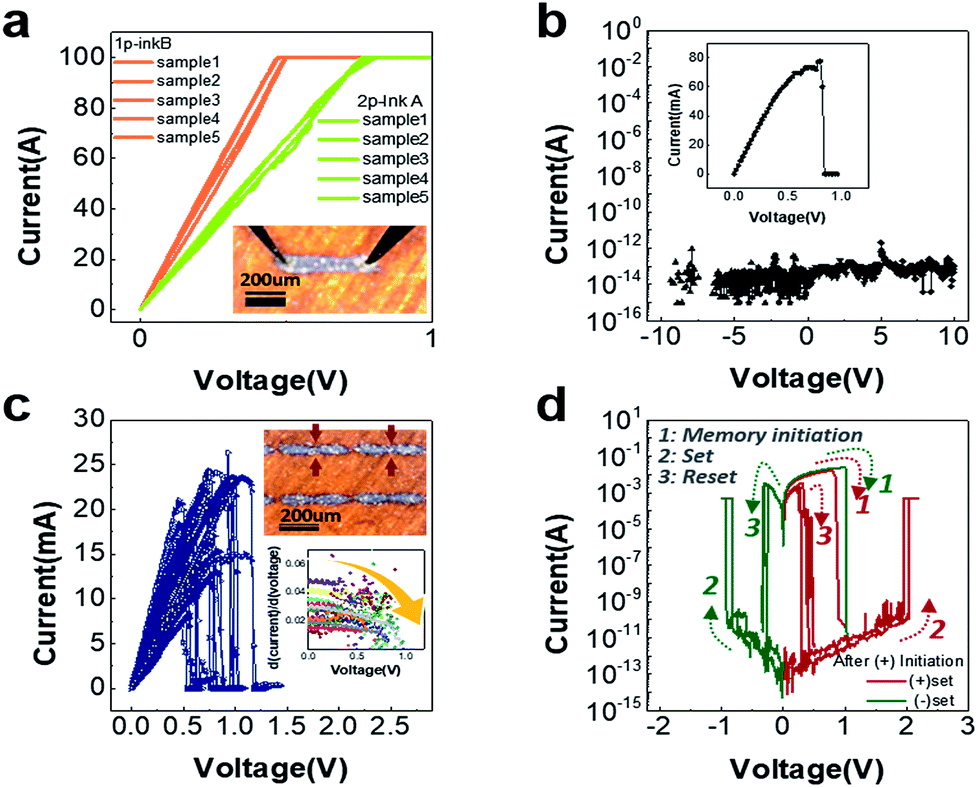 | ||
| Fig. 1 (a) Successful metal sintering in a twice-printed Ag nanoparticle ink A (2p-inkA) and a single pass printed ink B (1p-inkB). Inset figure shows the planar device structure of a 2p-inkA device. (b) Set failure in an hourglass-shaped 1p-ink B device. (c) Initial metal rupture before resistive switching takes place in hourglass-shaped 2p-ink A devices. Optical microscope image of the hourglass devices, where the narrowest part is marked with the red arrows (inset). (d) Typical non-polar resistive switching in the hourglass shape memristor devices after going through the initiation process described in (c). | ||
Results and discussion
The I–V characteristics in Fig. 1a show that the printed metal nanoparticles have been completely sintered during the post-drying and annealing process, showing uniformity in the device-to-device distribution on the polyimide flexible substrate. The inset of Fig. 1a is an optical image of a planar 2p-ink A device. 1p-inkB was fabricated in exactly the same shape, with no visible difference to the device shown in the Fig. 1a inset based on the optical microscope observation. Despite the single-pass printing, ink B shows slightly smaller resistance (∼5 Ω) compared to ink A with 2-pass printing (∼8 Ω). The resistances of single-pass printed ink A (1p-inkA) were slightly high and not as uniform as the others (ESI Fig. S1a†) implying that they are somewhat incompletely and stochastically sintered, possibly due to the low nanoparticle composition. Intriguingly, as shown in ESI Fig. S1,† several devices commonly encountered abrupt rupture of their metallic properties, and once ruptured, the devices showed a reversible resistive switching upon additional voltage application. This phenomenon could originate from reversible fuse and anti-fuse of the silver nanoparticles at a certain region of the device where the device suffers from locally enhanced Joule heating. Such local heating could be possibly caused by the incomplete sintering and hence the non-uniform resistance across the device.Based on these findings, resistive switching was also attempted with metallic 1p-inkB and 2p-inkA through a novel design of the device geometry. An hourglass-shaped pattern was fabricated so that the resistance could be locally enhanced in the bottleneck region with a narrow gap (50–70 μm) between two 200 μm-long planar ends. The resulting bottleneck region had various widths ranging from 20 to 50 μm, due to the inherent stochasticity of the printer. The bottleneck parts are indicated with red arrows in the inset of Fig. 1c. Both in the planar and hourglass shaped devices, the left-electrode was biased while the right electrode was grounded. This geometry allows spatially confined resistive switching, which is necessary for conducting related analysis as well as for implementing the devices into a memory array. As a result, the rupture of pristine metallic behaviour, which was seen only in the high resistance planar devices (1p-inkA) above, occurred even in these hourglass shape devices made from the 2p-inkA and 1p-inkB conditions. However, as shown in Fig. 1b, the 1p-inkB with its smaller resistances in the planar device form showed the initial rupture process at a high current level over 50 mA. The device stayed in its insulating state afterward even with the high voltage application up to ±10 V, meaning that no resistive switching is possible under this condition. The fabricated pristine device in this work is a metallic conductor, whereas the oxide-based RRAM or ECM usually has a pristine insulation state, so the initial rupture process corresponds to the electroforming process.
In contrast, Fig. 1c shows the metallic behaviour of 2p-inkA device ruptured by a relatively low current between 10 mA and 30 mA, and a reliable successive resistive switching behaviour is seen in Fig. 1d. According to the multiple current–voltage (I–V) curves of the initial metal rupture in the hourglass shape 2p-inkA devices, the slope of the I–V curves commonly decreases at the verge of the rupture event as seen in the inset of Fig. 1c. This provides evidence for the Joule heating effect along with the high current flow, which is accompanied by the gradual increase in its metallic resistance, immediately before the rupture. The resistance of a metal linearly increases with temperature, being proportional to the characteristic thermal coefficient of the metal. Since the amount of Joule heating (=I2R) is proportional to the resistance when a constant current flows through the devices, the bottleneck part of the hourglass shape is likely to become the favorable part for such metal rupture to take place. Fig. 1d shows typical resistive switching I–V curves of the hourglass 2p-inkA devices after an initial metal rupture event. The red and green curves represent switching with positive and negative bias polarities respectively in the devices where the initiation, i.e., the initial metal rupture, is performed under the positive bias condition. A compliance current value of 500 mA was applied during set operations to avoid the permanent breakdown of its insulating state and to resume the reversible resistive switching between the low and high resistance states. Due to the much higher metallic resistance after a set process relative to the pristine state, the following set processes are attributed to only a partial recovery from its metallic nature. This is most likely due to the rejuvenation of nanofilaments according to the migration of silver nanoparticles at the initially ruptured region of the device. The detailed switching mechanisms are discussed with the aid of Fig. 3 and 4 later.
The present approach based on inkjet printing is useful in effectively enhancing the local Joule heating. Fig. 2a through Fig. 2c provide scanning electron microscopy (SEM) and transmission electron microscopy (TEM) images revealing the geometry of an hourglass shape memristor device (2p-inkA) with the reduced lateral dimension of the bottleneck region (down to 20 μm) and the thickness of the Ag electrode (500 nm). For an accurate detection of the Ag thickness of the bottleneck region, a blanket 100 nm Pt layer was coated on top of the device to avoid severe charge accumulation on the polyimide substrate during focused ion beam (FIB) milling. The resultant cross-sectional TEM image in Fig. 2c reveals a 40–60 nm-thick polycrystalline Ag layer, for which a protrusion on the surface becomes the most preferred nucleation and growth site for the Ag cluster-filaments. The fabrication method of leaving a small gap between the planar Ag electrodes here has effectively reduced both the width and thickness at the bottleneck region. Based on the measured width and thickness of the electrode and bottleneck region, Fig. 2d shows the simulated temperature distribution across the entire device during the initial Ag metal rupture using COMSOL simulation (details given in ESI†). The electrical conductivity (2 × 10⁶ S m−1) and the average current level (20 mA) at the verge of metal rupture were extracted from Fig. 1a and c. The substrate is not shown in the device model image of Fig. 2d for simplicity. The hourglass device with only the narrower width (20 μm) in its bottleneck region (upper right corner of Fig. 2d) shows a small increase (about 5 °C) in its temperature above the ambient of 20 °C. However, the device with both narrower (20 μm) and thinner (50 nm) dimension of Ag metal in its bottleneck region shows more than the 100 °C increase within the region. The width and thickness of other parts are 80 μm and 500 nm, respectively. Such a dramatic thickness modulation across a single device is possible through a one-step printing described here, which otherwise would have required complex lithography and etching steps. The experimental result from a thermal emission measurement shown in Fig. 2e provides a consistent spatial temperature distribution on the device when applying a short AC pulse. Here, a 20 V high pulse height and 30 ns pulse duration were adopted to produce sufficient heat generation within the detectable range. Although the instrument does not provide the exactly calibrated temperature, the hottest spot is obviously placed within the bottleneck region, midway between the contact probes. Once the temperature on the hot spot exceeds a certain level that Ag can endure, the spot is supposed to turn into an insulator (Ag2O).
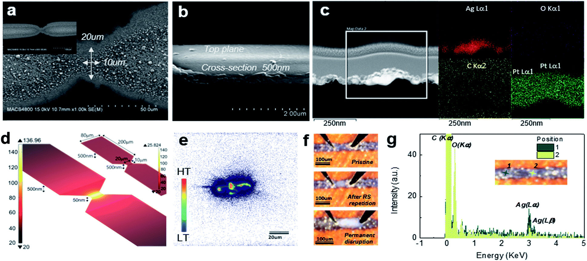 | ||
| Fig. 2 (a) Top-view SEM image of the bottleneck part, (b) cross-sectional SEM image of the planar electrode part, (c) cross-sectional TEM-EDX image of the bottleneck part of an hourglass shape memristor device. (d) The simulated temperature increases in the hourglass shape device based on the geometry observed by the microscopy images, (a) through (c). Inset is the simulated result assuming a geometry that has a uniform thickness across the entire device, i.e., both the electrode and bottleneck part. The local temperature increase is mostly attributed to much thinner Ag of the bottleneck part compared to that of the electrode part. (e) Experimental evidence of the local temperature increase confined in the bottleneck region observed by a thermal emission detection measurement. (f) Optical microscope image of a pristine hourglass shape memristor (top), the device after going through tens of switching cycles (middle), and a device that showed abnormally high metal rupture current and no following switching behavior (bottom). (g) EDS analysis at position 1 (bottleneck) and 2 (electrode). | ||
The upper and middle panels of Fig. 2f show an optical microscopy image of the memristor device prior to and after tens of repetitive switching cycles, respectively. Specifically, the bottleneck region after the switching shows an obvious configurational change from its pristine state. This further confirms that the resistive switching in the hourglass shape device takes place at that part of the device, as intended. Fig. 2g shows EDX (energy-dispersive X-ray spectroscopy) energy spectrum results for the bottleneck region after resistive switching and the other intact metal region. Each position on the device is indicated by a dark and light green mark in the inset device image. The bottleneck region has higher (lower) oxygen (Ag) concentration compared with the metal electrode position. Therefore, it can be postulated that the initial metal rupture generates an oxide layer, most likely a silver oxide, and the switching occurs according to the interplay between the electrode as cation source and the oxide insulator that simultaneously serves as an ionic conductor for the cation migration. Ag2O is the most common form of silver oxide, generated easily when silver is exposed to oxygen in the ambient temperature. It is known that the thickness of the oxide increases with temperature up to a certain value, after which the oxide starts to decompose into silver and oxygen.43,44 The oxide decomposition temperature ranges from 500–700 K in air, depending on the film thickness and fabrication method. A conductive silver device is generated during fabrication owing to the annealing temperature, low enough to avoid any silver oxide generation. Upon biasing, however, Joule heating will increase the temperature, generating the insulating silver oxide at the weakest part of the hourglass device. Once enough silver oxide is available to block the current flow, it will prevent further Joule heating so that a stable insulating state is retained. This is reflected in the I–V curves of the initiation process (Fig. 1c), where the current stays at lower value once the rupture of the conducting state happens. In contrast, the lowest panel of Fig. 2f shows one peculiar case, where the device has gone through the initial metal rupture with a very high current almost up to 100 mA, mainly due to an abnormally thick bottleneck part. No resistive switching followed in such high current induced rupture case, whose insulating state featured an order of magnitude lower current level than those from the other cases (ESI Fig. S1c†). As shown in the figure, the resulting change at the bottleneck is much more severe. Therefore, it can be concluded that just like in the above-mentioned hourglass 1p-inkB case (Fig. 1b), some of the 2p-inkA devices with anomalously large bottleneck cross-section cannot initiate subsequent resistive switching despite the obvious metal rupture event, due to the excessive energy applied during the rupture. Such huge energy consumption would generate too thick an insulator (rupture region) as shown in the lowest panel of Fig. 2f so that even a high voltage up to ±10 V cannot trigger the Ag nanoparticle migration within the insulator layer. There could also be a possibility that the high energy consumption might have resulted in a too stoichiometric insulator, which does not contain sufficient defect sites for the cations to migrate through.
Fig. 3a shows reliable unipolar resistive switching (URS) at both bias polarities for the 2p-inkA device. An on/off ratio over 108 at a reading voltage of 0.02 V is attained irrespective of the switching polarities. This kind of unipolar resistive switching is often alternatively referred as non-polar resistive switching, implying that the switching is hardly influenced by the polarity of the applied electric field. Instead, the mechanism relies on the size of the power consumed during the switching, originated from Joule heating. Typically phase change mechanism (PCM) and thermochemical mechanism (TCM) correspond to this type of behaviour. The former involves a transition between the amorphous and crystalline phases of certain chalcogenide materials, widely adopted for phase change random access memory (PRAM), which has little relevance to the oxide switching matrix here. Instead, it is likely that the present non-polar resistive switching phenomenon occurs based on generation and Joule heating-induced rupture of the Ag filaments within the Ag2O switching matrix, that is, close to TCM. This is normally accompanied by an abrupt set and reset operation, which is consistent with Fig. 3a. A set voltage is the voltage required to incur electric field-induced Ag cation migration within the switching matrix and as they become reduced and accumulated within the insulator, Ag metallic filament is generated bridging the two metal electrode portions. On the other hand, reset is attributed to the thermally activated diffusion of the Ag metal clusters, thus normally accompanied with the high current flow, which is even higher than the maximum current limit or compliance current assigned during its preceding set process (see Fig. 3a and b).
 | ||
| Fig. 3 (a) I–V curves of unipolar resistive switching (URS) operation at positive bias polarity (left) and negative bias polarity (right) of the memristor device. (b) Proposed Ag mobile ion distribution after a ‘positively’ biased initial metal rupture (left). Conically shaped nanofilament generation by a negatively biased set and hourglass shaped nanofilament generated by positively biased set (right). (c) Simulated temperature and electric field distributions for the hourglass and conical shape nanofilaments. The temperature increase overrides the electric field effect in an hourglass filament, whereas the electric field dominates in the conical filament. (d) Schematic diagram of the devices during a positive bias and negative bias URS. Both URS operations rely on thermal rupture of the filaments, presumably due to the isotropic diffusion or dissolution of Ag particles into the oxide electrolyte. However, due to its strong electric field, the conical shape is likely to go through an evolution toward an hourglass shape before it becomes ruptured. | ||
There is, however, a characteristic difference in the switching behaviours depending on the bias polarity, as shown in Fig. 3a. When the device was initially ruptured and subsequently switched with a positive bias, the set state showed mostly simple ohmic behaviour (reset curves of left-hand panel of Fig. 3a). In contrast, when the device was initially ruptured with a positive bias but subsequently operated with a negative bias, the set state showed additional change as indicated by the “secondary set” in the right-hand panel of the same figure. The on-state resistance decreases at ∼0.15 V in the negative bias set case, meaning that an additional set switching occurs at this voltage during each reset cycle. This can be comprehended in conjunction with the adopted bias polarity during the initiation, which should have led to asymmetry in the initial distribution of mobile Ag nanoparticles within the switching matrix. Since these devices are positively biased during the initial metal rupture stage, most of the Ag cations are likely to move toward the other side (right electrode, RE) of the positively biased electrode (left electrode, LE) during the rupture, as described in the schematic diagram of Fig. 3b. Given this initial asymmetric Ag distribution within the insulator, the negative bias can generate an Ag filament once a little portion of the mobile ions segregated at the RE side reaches the LE side. That is, a conical shape filament having the smallest radius in the vicinity of LE is generated. On the other hand, since the additional Ag cations should be introduced through the oxidation of the LE during the positive bias set, an hourglass shape Ag filament that has the smallest radius in the middle of the switching matrix is likely to be generated.
Such a model based on the different filament geometry originating from the asymmetric initial nanoparticle distribution is further supported by a simulated thermo-field distribution shown in Fig. 3c. The conical filament (right-hand panel) was assumed to be comprised of a few atoms for its minimum radius (3 nm), and a slightly larger minimum cross-section (5 nm) was assumed for the hourglass filament (left-hand panel). This is because a larger amount of Ag nanoparticles should be involved to form the hourglass filament due to the additional incorporation of Ag nanoparticles into the oxide layer. This is further supported by the larger positive bias set voltages than the negative set bias voltages, which implies that the positive bias set kinetics involves the additional dissolution of relatively stable Ag electrode particles into the oxide. Although the geometric parameters on the active switching region are unknown, a direct comparison between the two cases can be made by considering the plausible parametric range based on previous reports. The detailed simulation environment is given in ESI Section 2.† The comparison reveals that the thermal and electric field effects are predominant in the hourglass and conical filament, respectively. As shown in the schematic diagram of Fig. 3d, an hourglass shape filament generated by the positive set bias is immediately ruptured once it reaches enough temperature for its isotropic dissolution back into the oxide switching matrix, or rupture. However, the conical shape filament incurred by a negative set suffers from the strong electric field that leverages the additional redox reaction of the Ag filament. Tracing the direction of the electric field represented by the black arrows in the conical shape (bottom right panel of Fig. 3c), the additional Ag migration would eventually cause the evolution of the conical filament toward an hourglass shape before it reaches enough temperature required for its thermal rupture. This is reflected by the secondary set process in its I–V behaviour before its reset process takes place (right panel of Fig. 3a). The proximity of the narrowest region of the conical filament to the bulk electrode region incurs heat loss, so the thermal effect has less significance than the other case.
Surprisingly enough, despite the symmetric device structure and silver electrode at both sides, bipolar operation is also available in this system, likely due to the asymmetric nanoparticle distribution introduced at the electrical switching initiation process. In Fig. 4a, the set and reset are accomplished at the negative and positive bias polarities, respectively. This operation mode is beneficial in decreasing the switching current (and power too). As shown in Fig. 4b, the switching is done with lower reset current (Imax,reset) than the compliance current assigned during the preceding set operations, which was not the case in the URS operations of Fig. 3. This is because reset is mainly governed by the electric field induced oxidation, whereas it is due to thermal rupture in URS, and thus, is comparable to the conventional ECM. The schematic diagrams describing each switching step are included in the insets of Fig. 4a. Based on its much smaller operation current (Fig. 4b) and write voltage below 0.5 V (the inset of Fig. 4c), the present memristor in its bipolar scheme is the most feasible candidate for the printed non-volatile memory application. There is also a clear distinction between the set and reset voltages, which was not the case for URS in Fig. 3. The cycle endurance of the memory operation lasted over 100 cycles even in the harsh DC measurement mode, implying it could last much longer if applied with much shorter AC pulse switching. Despite the DC bias limited endurance, it is still competitive to its metal oxide counterparts on flexible substrates.35,36 The non-volatile characteristics of both memory states lasted over 3 × 10⁴ s at room temperature. The seemingly unstable high resistance state, in fact, comes from the measurement limit of the instrument, which cannot give accurate data below 10−13 A.
 | ||
| Fig. 4 (a) I–V curves of bipolar memristor operation and the corresponding schematics for each switching step (insets). (b) Maximum current during the reset process (Imax,reset) of each switching mode. The bipolar operation features reset current smaller than the current compliance (Icc,set), which supports the typical redox reaction based switching mechanism, i.e., electrochemical metallization. (c) Endurance and (d) retention characteristics of the bipolar switching mode. Both set and reset voltage size lower than 0.5 V implies for the promising power efficient printed memristor operation (inset of (c)). (e) Volatile threshold switching behavior of the memristor. | ||
As opposed to the conventional electrochemical metallization (ECM) theory, where two electrodes are different as an active (Ag, Cu) and an inert (Pt, Au) metal to enable bipolar switching, the present device performs a robust bipolar operation despite its symmetric electrode adoption with active metals at both sides. And this can be successfully understood in conjunction with the asymmetric nanoparticle distribution secured during the initiation process and the resulting uneven electric field distribution across the filament. The proposed model assumes the Ag nanofilament growth beginning from the cathode to anode, generating a conical filament that has richer nanoparticle composition near the anode side. In fact, the filament growth beginning from the cathode side has been a norm in the conventional ECM theory, as the cations can immediately migrate toward the cathode in the electrolyte and the filament growth kinetics is mainly governed by the redox reaction of the cathode/electrolyte interface. Unlike in the conventional electrolytes such as Ag2S and chalcogenide materials, however, the filament growth within the Ag2O oxide electrolyte is postulated to be limited by the low ion mobility of the electrolyte. Such a conical shape metal filament with richer Ag nanoparticles in its anode side has been directly observed previously using in situ TEM,41 further supporting the present switching model described above. Due to the presence of trapped electrons or the electrons injected into the oxide electrolyte, the Ag cations have higher chance of being reduced before reaching the cathode side.42
Besides non-volatile resistive switching, a volatile resistive switching, namely threshold switching, is also performed by adjusting a compliance current below 50 μA during the set operation, as in Fig. 4e. Despite the obvious set transition or abrupt current jump in the I–V curve, the device remains in the off state in the following voltage sweep at voltage level < holding voltage (Vhold) under the compliance current fixed at 10 μA. Under such a small compliance current, a relatively weak Ag filament comprised of a few Ag nanoclusters is generated and is readily ruptured by the thermal agitation once the electric field is removed. The filament relaxation back to the Ag nano-particles has recently been verified through in situ TEM observation, and it was ascribed to the Ostwald ripening of the Ag clusters mainly to minimize the filament surface energy in the oxide switching matrix. This has little relevance to the previously described redox based mechanism of Ag ions for the non-volatile switching. Such Gibbs Thomson effect-induced threshold switching in the Ag electrode system is extensively studied for its bio-mimicking capability and sensor applications.45–48 From a double-sweep result, where the voltage is gradually increased and then sequentially decreased, the minimum voltage at which the device remains on state, Vhold, is evaluated. It is slightly above 0 V, and such a small Vhold is highly favourable for selector application of the crossbar array architecture. Two-terminal selectors, as well as non-volatile memory components, are essential components for the ultra-high density crossbar memory. Typical two-terminal selectors include threshold switch and diode with high I–V non-linearity or rectifying property, by which the sneak (leakage) currents within the crossbar architecture can be impeded. Moreover, this type of volatile switching element is highly promising for the emulation of synaptic learning, when combined with an appropriate non-volatile switching element that operates in an analog manner.12
Conclusions
An hourglass-shaped inkjet-printed Ag nanocluster pattern has been shown to enable memristor operation after an initial rupture of its pristine metallic state via high current flow through the device. The inkjet printing method is very efficient for flexible electronics, as it does not require additional lithography or etching steps to accomplish the desired geometrical deformation of the device. In addition, the metal-oxide electrolyte-metal system is generated here with only a single metal ink and creating the active layer in situ through Joule heating and rupturing in the bottleneck region of the hourglass shape device. The chemical analysis in this region reveals that the Joule heating leads to severe oxidation of the Ag nanoparticles into Ag2O insulator. Within the Ag2O switching matrix, the generation and rupture of Ag filaments according to the size and polarity of the applied electric field lead to the resistive switching behavior. The initial Ag nanoparticle distribution that is determined by the bias polarity applied during the initial metal rupture stage supports the subsequent asymmetry about the switching polarities. The corresponding switching mechanisms for various switching characteristics ranging from unipolar/bipolar non-volatile switching to threshold switching, all in a controllable manner, were postulated considering both the Joule heating and electric field induced filament dissolution. The electrical method of initiating memristor behavior from the simple printed electrode pattern simplifies the fabrication efforts for printing all the functioning MIM layers and the demanding ink formulation of each individual layer material. Such convenience for attaining the versatile inkjet printed memristors will further pave the way toward their application in the future low-power applications on flexible substrates.Conflicts of interest
The authors declare no competing financial interest.Acknowledgements
This work was supported in part by the In-Space Manufacturing Program of the Advanced Exploration Systems Office of the NASA HEOMD. The work in Korea was supported by the Global Research Laboratory Program (No. NRF-2012K1A1A2040157) of the Ministry of Science, ICT, and Future Planning of the Republic of Korea. The authors are grateful to Niki Werkheiser, Curtis Hill and Jessica Koehne for their support. JH, DM, and MS are with University Space Research Association, and their work was supported by a NASA contract to USRA.References
- L. Chua, IEEE Trans. Circuit Theory, 1971, 18, 507–519 Search PubMed.
- D. B. Strukov, G. S. Snider, D. R. Stewart and R. S. Williams, Nature, 2008, 453, 80–83 CrossRef CAS PubMed.
- J. J. Yang, D. B. Strukov and D. R. Stewart, Nat. Nanotechnol., 2013, 8, 13–24 CrossRef CAS PubMed.
- D. S. Jeong, K. M. Kim, S. Kim, B. J. Choi and C. S. Hwang, Adv. Electron. Mater., 2016, 2, 1600090 CrossRef.
- C. S. Hwang, Adv. Electron. Mater., 2015, 1, 1400056 CrossRef.
- G. Wang, A. C. Lauchner, J. Lin, D. Natelson, K. V. Palem and J. M. Tour, Adv. Mater., 2013, 25, 4789–4793 CrossRef CAS PubMed.
- G. H. Kim, J. H. Lee, Y. Ahn, W. Jeon, S. J. Song, J. Y. Seok, J. H. Yoon, K. J. Yoon, T. J. Park and C. S. Hwang, Adv. Funct. Mater., 2013, 23, 1440–1449 CrossRef CAS.
- K. J. Yoon, G. H. Kim, S. Yoo, W. Bae, J. H. Yoon, T. H Park, D. E. Kwon, Y. J. Kwon, H. J. Kim and Y. M. Kim, Adv. Electron. Mater., 2017, 3, 1600326 Search PubMed.
- J. Borghetti, G. S. Snider, P. J. Kuekes, J. J. Yang, D. R. Stewart and R. S. Williams, Nature, 2010, 464, 873–876 CrossRef CAS PubMed.
- P. Huang, J. Kang, Y. Zhao, S. Chen, R. Han, Z. Zhou, Z. Chen, W. Ma, M. Li and L. Liu, Adv. Mater., 2016, 28, 9758–9764 CrossRef CAS PubMed.
- A. Siemon, T. Breuer, N. Aslam, S. Ferch, W. Kim, J. van den Hurk, V. Rana, S. Hoffmann-Eifert, R. Waser and S. Menzel, Adv. Funct. Mater., 2015, 25, 6414–6423 CrossRef CAS.
- Z. Wang, S. Joshi, S. E. Savel'ev, H. Jiang, R. Midya, P. Lin, M. Hu, N. Ge, J. P. Strachan and Z. Li, Nat. Mater., 2017, 16, 101–108 CrossRef CAS PubMed.
- M. Prezioso, F. Merrikh-Bayat, B. Hoskins, G. Adam, K. K. Likharev and D. B. Strukov, Nature, 2015, 521, 61–64 CrossRef CAS PubMed.
- F. Alibart, E. Zamanidoost and D. B. Strukov, Nat. Commun., 2013, 4, 2072 CrossRef PubMed.
- S. T. Han, Y. Zhou and V. Roy, Adv. Mater., 2013, 25, 5425–5449 CrossRef CAS PubMed.
- K. Qian, V. C. Nguyen, T. Chen and P. S. Lee, J. Mater. Chem. C, 2016, 4, 9637–9645 RSC.
- L. Gonzalez-Macia, A. Morrin, M. R. Smyth and A. J. Killard, Analyst, 2010, 135, 845–867 RSC.
- M. Gao, L. Li and Y. Song, J. Mater. Chem. C, 2017, 5, 2971–2993 RSC.
- J. H. Cho, J. Lee, Y. Xia, B. Kim, Y. He, M. J. Renn, T. P. Lodge and C. D. Frisbie, Nat. Mater., 2008, 7, 900–906 CrossRef CAS PubMed.
- J. Li, F. Rossignol and J. Macdonald, Lab Chip, 2015, 15, 2538–2558 RSC.
- A. Vlad, N. Singh, C. Galande and P. M. Ajayan, Adv. Energy Mater., 2015, 5, 1402115 CrossRef.
- A. Teichler, J. Perelaer and U. S. Schubert, J. Mater. Chem. C, 2013, 1, 1910–1925 RSC.
- S. Nau, C. Wolf, K. Popovic, A. Blümel, F. Santoni, A. Gagliardi, A. di Carlo, S. Sax and E. J. List-Kratochvil, Adv. Electron. Mater., 2015, 1, 1500234 CrossRef.
- B. Cho, S. Song, Y. Ji, T. W. Kim and T. Lee, Adv. Funct. Mater., 2011, 21, 2806–2829 CrossRef CAS.
- Z. Wang, F. Zeng, J. Yang, C. Chen and F. Pan, ACS Appl. Mater. Interfaces, 2012, 4, 447–453 CrossRef CAS PubMed.
- U. S. Bhansali, M. A. Khan, D. Cha, M. N. AlMadhoun, R. Li, L. Chen, A. Amassian, I. N. Odeh and H. N. Alshareef, ACS Nano, 2013, 7, 10518–10524 CrossRef CAS PubMed.
- P. Heremans, G. H. Gelinck, R. Muller, K.-J. Baeg, D.-Y. Kim and Y.-Y. Noh, J. Mater. Chem., 2010, 23, 341–358 CrossRef.
- G. Khurana, P. Misra and R. S. Katiyar, Carbon, 2014, 76, 341–347 CrossRef CAS.
- R. Waser, R. Dittmann, G. Staikov and K. Szot, Adv. Mater., 2009, 21, 2632–2663 CrossRef CAS.
- K. M. Kim, D. S. Jeong and C. S. Hwang, Nanotechnology, 2011, 22, 254002 CrossRef PubMed.
- J. Jang, H. Kang, H. C. N. Chakravarthula and V. Subramanian, Adv. Electron. Mater., 2015, 1, 1500086 CrossRef.
- D.-H. Lien, Z.-K. Kao, T.-H. Huang, Y.-C. Liao, S.-C. Lee and J.-H. He, ACS Nano, 2014, 8, 7613–7619 CrossRef CAS PubMed.
- G. Vescio, J. López-Vidrier, R. Leghrib, A. Cornet and A. Cirera, J. Mater. Chem. C, 2016, 4, 1804–1812 RSC.
- P. Vilmi, M. Nelo, J.-V. Voutilainen, J. Palosaari, J. Pörhönen, S. Tuukkanen, H. Jantunen, J. Juuti and T. Fabritius, Flexible Printed Electron., 2016, 1, 025002 CrossRef.
- G. Vescio, A. Crespo-Yepes, D. Alonso, S. Claramunt, M. Porti, R. Rodriguez, A. Cornet, A. Cirera, M. Nafria and X. Aymerich, IEEE Electron Device Lett., 2017, 38, 457–460 CAS.
- S. Zou and C. Michael, Electronic Components and Technology Conference, 2014, pp. 441–446 Search PubMed.
- C.-C. Yu, J. D. Baek, C.-H. Su, L. Fan, J. Wei, Y.-C. Liao and P.-C. Su, ACS Appl. Mater. Interfaces, 2016, 8, 10343–10349 CrossRef CAS PubMed.
- J.-H. Park, M.-J. Park and J.-S. Lee, Nanoscale, 2017, 9, 555–561 RSC.
- J. Lee, S. Chung, H. Song, S. Kim and Y. Hong, J. Phys. D: Appl. Phys., 2013, 46, 105305 CrossRef.
- S. Chung, J. Lee, H. Song, S. Kim, J. Jeong and Y. Hong, Appl. Phys. Lett., 2011, 98, 153110 CrossRef.
- U. Celano, L. Goux, A. Belmonte, K. Opsomer, A. Franquet, A. Schulze, C. Detavernier, O. Richard, H. Bender and M. Jurczak, Nano Lett., 2014, 14, 2401–2406 CrossRef CAS PubMed.
- Y. Yang, P. Gao, S. Gaba, T. Chang, X. Pan and W. Lu, Nat. Commun., 2012, 732 CrossRef PubMed.
- G. I. N. Waterhouse, G. A. Bowmaker and J. B. Metsona, Phys. Chem. Chem. Phys., 2001, 3, 3838–3845 RSC.
- M. L. Zheludkevich, A. G. Gusakov, A. G. Voropaev, A. A. Vecher, E. N. Kozyrski and S. A. Raspopov, Oxid. Met., 2004, 61, 39–48 CrossRef CAS.
- R. Midya, Z. Wang, J. Zhang, S. E. Savel'ev, C. Li, M. Rao, M. H. Jang, S. Joshi, H. Jiang and P. Lin, Adv. Mater., 2017, 29, 1604457 CrossRef PubMed.
- Z. Wang, S. Joshi, S. E. Savel'ev, H. Jiang, R. Midya, P. Lin, M. Hu, N. Ge, J. P. Strachan, Z. Li, Q. Wu, M. Barnell, G.-L. Li, H. L. Xin, R. S. Williams, Q. Xia and J. J. Yang, Nat. Mater., 2017, 16, 101–108 CrossRef CAS PubMed.
- J. H. Yoon, Z. Wang, K. M. Kim, H. Wu, V. Ravichandran, Q. Xia, C. S. Hwang and J. Joshua Yang, Nat. Commun., 2018, 9, 417 CrossRef PubMed.
- M. Wang, Adv. Mater., 2018, 30, 1802516 CrossRef PubMed.
Footnote |
| † Electronic supplementary information (ESI) available. See DOI: 10.1039/c9na00329k |
| This journal is © The Royal Society of Chemistry 2019 |