
 Open Access Article
 This Open Access Article is licensed under a Creative Commons Attribution-Non Commercial 3.0 Unported Licence
Structural color printing with a dielectric layer coated on a nanotextured metal substrate: simulation and experiment†
Minseok
Seo
a,
Heungyeol
Lee
b,
Hohyeong
Kim
b and
Myeongkyu
Lee
 *a
*a
aDepartment of Materials Science and Engineering, Yonsei University, Seoul 120-749, Korea. E-mail: myeong@yonsei.ac.kr
bKorea Institute of Industrial Technology, Incheon 21999, Korea
First published on 3rd September 2019
Abstract
The printing of plasmonic structural colors relies on noble metal nanostructures fabricated on Si, glass, or plastic substrates. This paper presents a simple surface structure for producing vivid structural colors directly from common metal substrates. The structure is formed by texturing the surface of stainless steel (STS) via imprinting and coating it with a dielectric layer. Diverse colors are generated simply by varying the thickness of the dielectric layer. The colors arise from surface plasmon resonance and guided-mode resonance of the incident light, which are excited on the textured STS surface and inside the dielectric layer, respectively. A finite-difference time-domain simulation shows that 500 nm is the optimum texture periodicity with regard to the tunability and vividness of the colors. This is experimentally verified by printing many differently colored images on the surface of STS substrates with a texture period of 500 nm. The proposed structure/method does not require a nanofabrication technique such as electron-beam lithography or focused ion beam etching. The results of the study provide a facile route for producing vivid structural colors on metals, which may find various applications, including surface decoration, product identification, anti-counterfeiting, and perfect absorbers.
Introduction
Structural colors emerge because of the interactions of light with surface structures.1–7 Fundamental optical processes such as reflection, refraction, interference, diffraction, and resonance account for the emergence of structural colors. The engineering of structural colors has drawn great interest in a variety of fields, such as photovoltaics,8,9 flat panel displays,10 sensors,11,12 product identification, and anti-forgery.13,14 Surfaces decorated with structural colors are also receiving considerable attention owing to their widespread use.15–18 Structural colors are easily observed in nature. The beautiful colors of bird feathers and butterfly wings may be the most brilliant and brightest structural colors in nature. Over the past decade, various artificial structures have been investigated to mimic the structural colors of living creatures, e.g., nanoparticle assemblies, multiscale structures, photonic crystals, diffraction gratings, and selective mirrors.14,19–25 However, the practical applications of these biomimetic structures are limited due to their complex fabrication processes and durability issues. Plasmonic colors are structural colors that arise from the resonant interactions between visible light and metal nanostructures.26–30 Color printing based on plasmonic nanostructures has attracted considerable attention owing to its broad potential applications.31–35 However, achieving plasmonic colors over large areas for practical use remains a challenge. Plasmonic nanostructures operating at visible wavelengths require subwavelength features and are typically fabricated using focused ion beam or electron-beam (e-beam) lithography. These nanofabrication techniques are neither economical nor scalable. Additionally, because the colors are tuned by tailoring the geometry and dimensions of the structure, nanostructures with different shapes and sizes are needed to produce different colors.Thus far, plasmonic color printing has mainly relied on noble-metal nanostructures fabricated on glass, Si, or plastic substrates. If plasmonic structures can be formed on common metal substrates without using nanofabrication techniques, the fabrication complexity and cost can be significantly reduced. In a recent study,15 we showed that structural colors could be produced by texturing the surface of stainless steel (STS) and subsequently coating it with a dielectric protective layer. This approach exploits the excitation of surface plasmon resonance (SPR) and guided-mode resonance (GMR), which occur on the STS surface and inside the dielectric layer, respectively. The demonstration of SPR on STS is encouraging in that STS, rather than noble metals such as Au and Ag, can be used for metal plasmonics. Nevertheless, many aspects of this SPR and GMR-based coloration remain unclear, including the effects of structural parameters such as the texture period and the refractive index and thickness of the dielectric layer. In the present study, we analyzed the effects of these structural parameters on the hue, saturation, and brightness of colors via a finite-difference time-domain (FDTD) simulation. The objective of this analysis was to identify optimum structures that maximize the color gamut. The effect of the texture period is particularly important because it ultimately determines the technique required to fabricate the surface structure. The FDTD simulation showed that 500 nm is the optimum texture period for the production of vivid colors over a wide tuning range. The surface of the STS substrates was one-dimensionally textured with this period via imprinting and etching and subsequently coated with a dielectric layer. Diverse colors were generated by varying the thickness of the dielectric layer; thus, the simulation results were experimentally verified. Additionally, color image patterns were printed by locally controlling the layer thickness. This study provides a promising route to print structural colors on STS and guidance for designing and producing colors on other metal substrates.
Results and discussion
Fig. 1 shows the structure used for the simulation, where a dielectric layer with refractive index n and thickness t is stacked on an STS substrate that has a one-dimensional (1D) surface grating with period p. Here, the dielectric-layer thickness t represents the thickness measured from the top surface of the grating. The duty cycle and height of the grating were fixed at 0.5 and 60 nm, respectively, and the grating was assumed to have a step-wise profile. Another assumption is that the surface of the dielectric layer was planar regardless of its thickness. The normal-incidence reflectance of the structure was simulated in the spectral range of 300–1000 nm. The simulation was performed under two different polarizations: transverse-electric (TE) and transverse-magnetic (TM). The periodic structure acts as a diffraction grating for light with wavelengths smaller than the grating period, dividing the incident light at these wavelengths into multiple beams. In the simulation, only 0th-order specular reflection was detected, and higher-order diffracted beams were filtered out to compare the simulation and experimental results more precisely. The period (p) of the grating and the refractive index (n) and thickness (t) of the dielectric layer were the three major parameters in the simulation. Although the reflection spectrum may also depend on other factors, such as the shape, aspect ratio, and duty cycle of the grating and the surface morphology of the dielectric layer, the three aforementioned parameters were expected to have dominant effects. The grating period was varied from 300 to 700 nm with intervals of 100 nm, and the layer thickness was varied with intervals of 10 nm. The complex refractive index, N = n + ik, of the experimentally used STS substrate was measured as a function of the photon energy by ellipsometry using a polished sample. The measured optical constants n and k were used for the FDTD simulation. Fig. S1 (ESI†) shows the real-part dielectric constant εm of the STS substrate, which was derived from the relation εm = n2 − k2. For the excitation of SPR, εm should be negative with its magnitude larger than the dielectric constant (1 for air and 4 for a dielectric medium with n = 2) of the surrounding medium. The frequency-dependent εm values measured for the STS substrate meet this requirement in the visible range.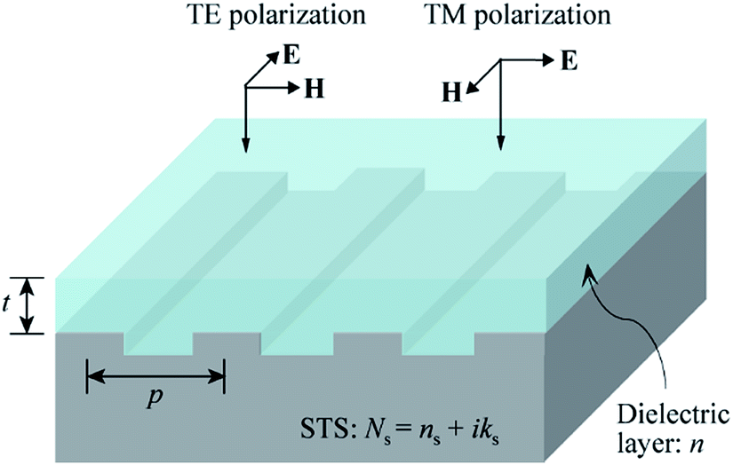 | ||
| Fig. 1 Structure used for the simulation. | ||
Fig. 2(a) shows the reflectance (R) of TE-polarized light with respect to the thickness of the dielectric layer and the wavelength (λ) of the light at three different grating periods: p = 300, 500, and 700 nm. The refractive index of the dielectric layer was n = 1.6. For p = 300 nm, the reflection spectrum was dominated by interference from the dielectric layer. A narrow resonance peak (i.e., a dip in reflectance) appeared in the range below 450 nm only when t exceeded 160 nm. As the grating period increased to p = 500 nm, this resonance peak red-shifted and became stronger, with an additional peak appearing for t > 200 nm. The wavelength of the resonance peak increased with t. The resonance branch line was red-shifted further at p = 700 nm. As shown in Fig. 2(a), the overall reflectance suddenly decreased at wavelengths smaller than the grating period. This is because higher-order diffracted beams were filtered out to obtain only the 0th-order specular reflection. The resonance peaks observed under TE polarization are attributed to GMR; the GMR branches are indicated by white dotted lines in Fig. 2(a). Fig. 3(a) shows the reflection spectrum obtained for p = 500 nm and t = 150 nm. A resonance peak was observed at λ = 603 nm. The electric field (E-field) profile at the resonance wavelength indicates that the field was mainly confined in the dielectric layer, representing a standing wave along the direction perpendicular to the grating grooves. GMR can be considered as a combination of the diffraction and waveguide.36–40 When the incident light is diffracted by the grating, the angle of a diffraction mode can match the angle of a guided mode supported by the dielectric layer, resulting in a resonance peak (i.e., a reflectance dip). Fig. 2(b) shows the reflectance of TM-polarized light with respect to t and λ at three different grating periods: p = 300, 500, and 700 nm. Here, the SPR branches are indicated by solid lines, and the GMR/SPR combined branches are indicated by long dotted lines. Fig. 3(b) shows the spectrum of TM-polarized light simulated with the same configuration (p = 500 nm and t = 150 nm). Two strong resonance peaks were observed. At λ = 821 nm, the magnetic field (H-field) was localized on the surface of the metal grating, confirming that the peak at this wavelength was due to SPR. The peak observed at a shorter wavelength of 519 nm was due to the combination of GMR and SPR. It is known that GMR and SPR can be simultaneously excited at a single wavelength.37,40Fig. 2 indicates that both TE and TM polarizations can support GMR, whereas SPR can be excited by TM-polarized light only. As the refractive index of the dielectric layer increased, a larger number of GMR, SPR, and combined modes were obtained. Fig. S2 (ESI†) presents the simulation results for n = 2.0.
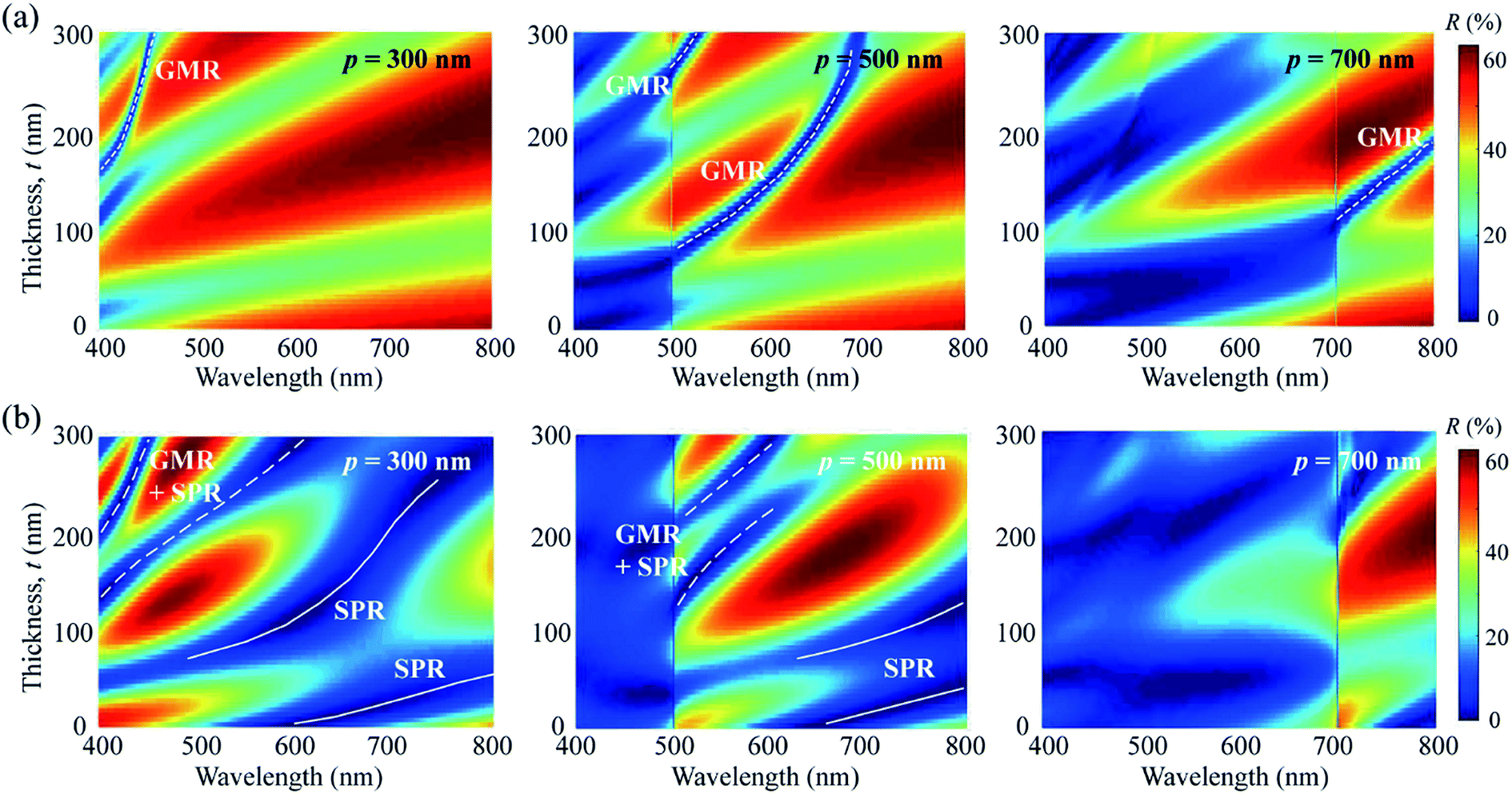 | ||
| Fig. 2 (a) Reflectance (R) of TE-polarized light with respect to the thickness of the dielectric layer and the wavelength of the light at three different grating periods: p = 300, 500, and 700 nm. (b) Reflectance of TM-polarized light. The refractive index of the dielectric layer is n = 1.6. | ||
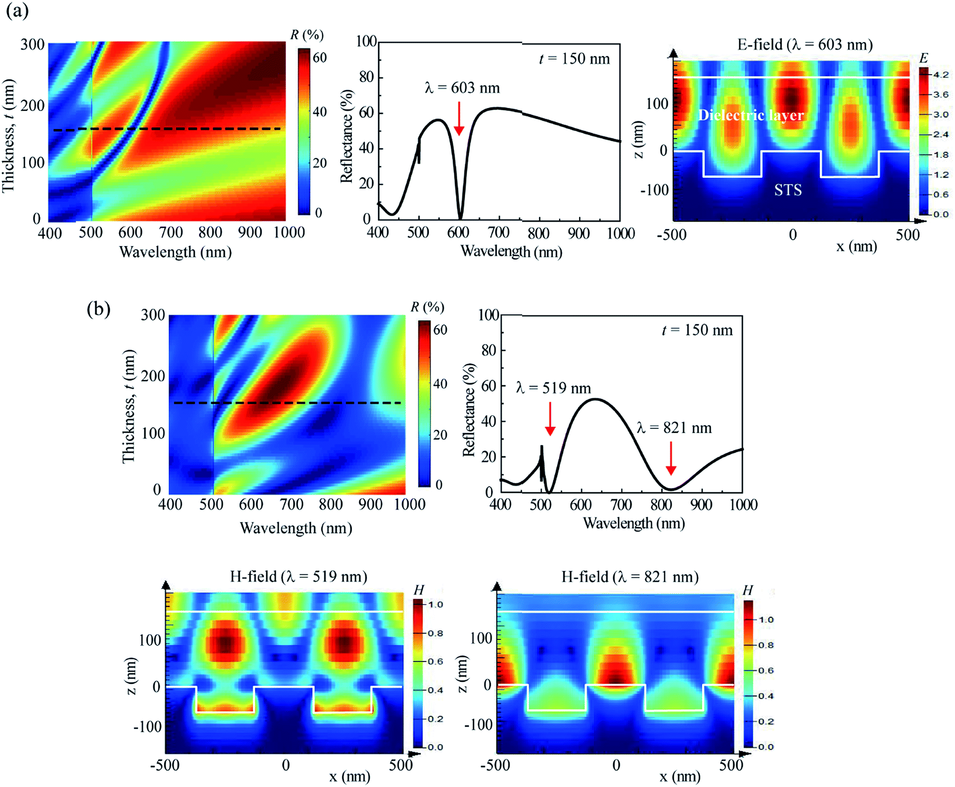 | ||
| Fig. 3 (a) Reflection spectrum simulated for p = 500 nm, n = 1.6, and t = 150 nm under TE polarization and the E-field profile at the resonant wavelength. (b) Spectrum of TM-polarized light obtained for the same configuration (p = 500 nm, n = 1.6, t = 150 nm) and the H-field profiles at the resonant wavelengths. | ||
Surface plasmons cannot be excited on a planar metal surface because the conservation of energy and momentum cannot be satisfied simultaneously. Therefore, a momentum transfer process is required to excite surface plasmons (i.e., to support SPR absorption). A periodic texture formed on the metal surface can act as a diffraction grating and thus transfer the momentum of incident light.41–43 However, SPR is supported only when the electric field of the incident light is parallel to the grating vector, which is perpendicular to the grating grooves.41–43 That is, SPR is supported by TM polarization only, and TE-polarized light does not produce any SPR peak. The coating of a dielectric layer onto the metal grating has two effects. First, it modifies the condition (i.e., wavelength) for SPR to occur. More importantly, it can excite GMR. As mentioned, GMR can be regarded as a combination of the diffraction and waveguide. When the metal grating is in close proximity to a dielectric slab waveguide, the incident light will be diffracted by the grating. If the angle of a diffraction mode matches the angle of a guided mode supported by the dielectric slab, a strong resonance called GMR occurs, resulting in a reflectance dip. GMR can take place under both TE and TM polarizations. All these account for the polarization-dependent optical responses (reflection spectra and colors) of the structure shown in Fig. 1. While the excitation of SPR and GMR is fundamentally enabled by the diffraction of incident light, and the far-field diffraction beams generated by the grating do not directly influence the colors observed under normal incidence because they spread out. Using colorimetric transformations, the reflection spectra were mapped to points on the CIE-1931 chromaticity diagram to determine the corresponding colors. Fig. 4 shows the dependence of the colors on the dielectric-layer thickness when n = 1.6. For p = 300 and 400 nm (Fig. 4(a) and (b), respectively), the colors revealed by TE-polarized light were not vivid. This is because the colors appearing at these grating periods were mainly due to an interference effect associated with the dielectric layer. As shown in Fig. 2(a), a GMR mode was located in the spectral range below λ = 450 nm at p = 300 nm. Therefore, it made a negligible contribution to the appearing colors. In contrast, when the grating period was increased to p = 600 and 700 nm (Fig. 4(d) and (e), respectively), the colors produced under TM polarization exhibited a limited tuning range. Additionally, they were very dark. As shown in Fig. 2(b), visible light incident on the grating with p = 700 nm had low specular reflectance owing to scattering by the grating. Thus, the amount of light captured in the far-field is small, making the produced colors dark. At p = 500 nm (Fig. 4(c)), a wide range of vivid colors was produced under both TE and TM polarizations, indicating that among the five different grating periods investigated, p = 500 nm was the optimum period with regard to the tunability and vividness of the colors. This has important practical implications. Because 500 nm is the minimum scale achievable via conventional photolithography, the fabrication of gratings with smaller periods requires nanofabrication techniques such as e-beam lithography and focused ion beam etching. Fig. 4 indicates that the colors can also be tuned by varying the period of the grating. In a recent study, this was demonstrated by forming transmission gratings with different periods via laser interference.44 However, color tuning by varying the thickness of the dielectric layer is even easier. Fig. S3 (ESI†) shows the color palette obtained for n = 2.0. The colors changed more quickly with the thickness of the dielectric layer because of the increased refractive index.
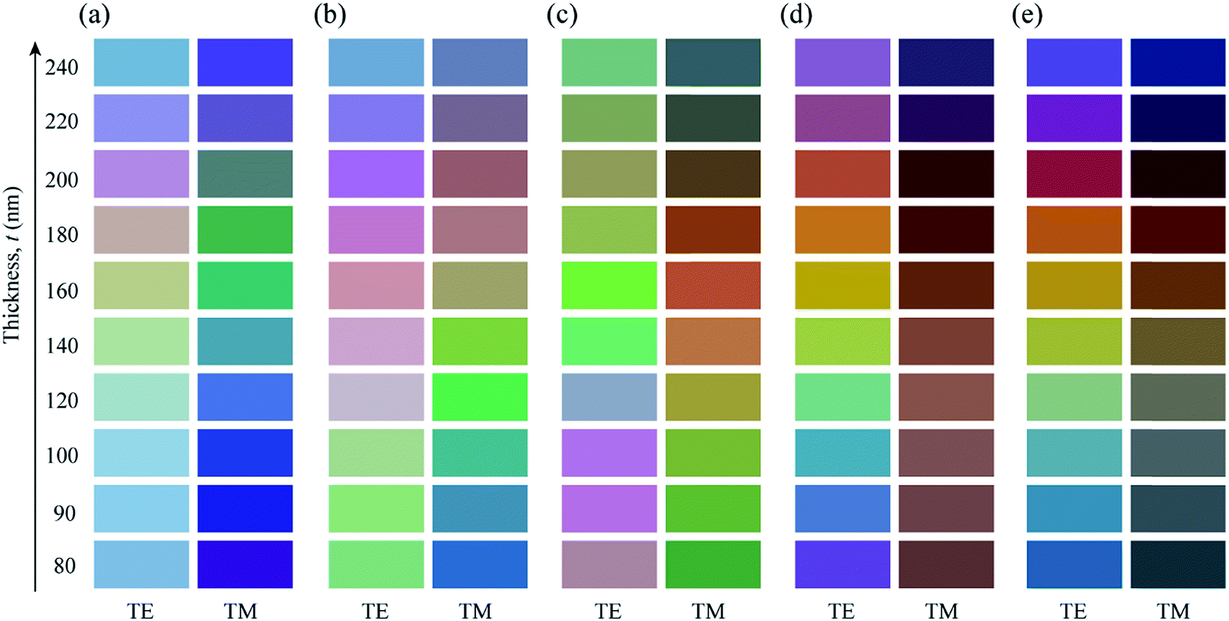 | ||
| Fig. 4 Colors with respect to the thickness of the dielectric layer for (a) p = 300 nm, (b) p = 400 nm, (c) p = 500 nm, (d) p = 600 nm, and (e) p = 700 nm. The refractive index of the dielectric layer is n = 1.6. | ||
To verify the simulation spectra and colors experimentally, 1D gratings with p = 500 nm were formed on the surface of STS substrates via imprinting and etching. The cross sections of the grating grooves were not perfectly rectangular but slightly tapered. The imprinting and etching conditions were adjusted so that the duty cycle and height of the gratings became ∼0.5 and ∼60 nm, respectively. Under-cut etching made it difficult to fabricate gratings with larger heights while maintaining the duty cycle at 0.5. Fig. S4 (ESI†) shows scanning electron microscopy (SEM) images of line patterns with different duty cycles and grating heights. All have the same period of 500 nm. The textured STS surface (duty cycle = 0.5 and grating height = ∼60 nm) was coated with a dielectric layer. SU-8 (n ≈ 1.6) and Si3N4 (n ≈ 2.0) were used as low- and high-index dielectric layers, respectively. The SU-8 layer was coated via spin coating, and the Si3N4 layer was coated via plasma-enhanced chemical vapor deposition. Fig. 5(a) compares the simulation and experimental spectra for n = 1.6 and t = 150 nm under TE polarization. The spectra under TM polarization are shown in the inset. The experimental spectra were obtained with a 150 nm-thick SU-8 layer coated onto the grating. While the TE-polarized experimental spectrum agreed well with the simulation spectrum, the TM-polarized spectrum (particularly the SPR peak appearing near λ = 750 nm) deviated from that predicted by the simulation. As discussed later, the TM spectra were more sensitive to the surface morphology of the dielectric layer than the TE spectra. Fig. 5(b) shows the experimental spectra obtained for a Si3N4 layer-coated STS substrate. Although the targeted thickness of the Si3N4 layer was 150 nm, the obtained spectra were similar to the spectra simulated for t = 130 nm and n = 2.0, indicating that the actual Si3N4 thickness was smaller than the target thickness. The dielectric layers on the planar and textured surfaces may have had slightly different thicknesses even though they were intended to have the same thickness.
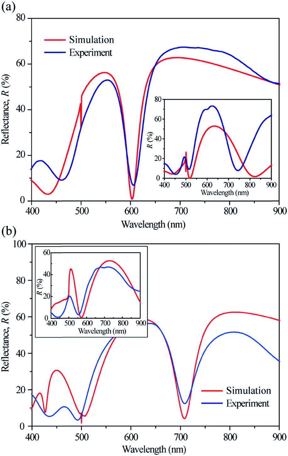 | ||
| Fig. 5 (a) Simulation and experimental spectra for n = 1.6 and t = 150 nm under TE polarization. The inset shows the spectra under TM polarization. The experimental spectra were obtained with a 150 nm-thick SU-8 layer coated onto the grating. (b) Simulation and experimental spectra for n = 2.0 and t = 130 nm under TE polarization. The inset shows the spectra under TM polarization. The experimental spectra were obtained with a Si3N4 layer coated onto the grating. | ||
The strong dependence of the colors on the thickness of the dielectric layer allows color images to be printed by locally controlling the layer thickness. Pressing the dielectric layer with a mold is probably the simplest method for printing color images. It is also favorable for mass production. In this case, the dielectric layer should be mechanically formable. Fig. 6(a) shows the images obtained by coating a SiO2 sol layer onto a textured STS substrate and then pressing it with a laser-fabricated glass mold. The images were captured using a digital camera after drying the pressed SiO2 film. The polarized images were taken by placing a linear polarizer between the camera and the sample. Fig. 6(b) shows the images printed in the same way with solution-coated SU-8 layers. The coated SU-8 films were polymerized after pressing. While the color of the images could be varied by adjusting the pressure applied to the mold, the images were mono-colored because the holes formed in the mold had identical depths. To print multi-colored images, the holes in the mold must have position-dependent depths. However, the fabrication of such a mold requires elaborate pattern designs and complicated processes. Another approach for printing color images is to selectively deposit the dielectric layer. The “maple leaf” images shown in Fig. 7 were printed by selectively depositing a Si3N4 layer using a shadow mask. After the textured STS surface was coated with a uniform Si3N4 layer, an additional Si3N4 layer was selectively deposited over it using a shadow mask. Thus, the background and image regions had different Si3N4 thicknesses, which are denoted as tb and ti, respectively. A variety of colors, including yellow, blue, green, scarlet, and purple, were produced by adjusting ti and tb. Different colors revealed under different polarizations may be effectively utilized for anti-counterfeiting. The tb and ti values shown in Fig. 7 are the target thicknesses set by the deposition system. The actual thicknesses, which were estimated by comparison with the simulation results, were smaller than the target thicknesses. Thus, the produced colors were different from those predicted by the simulation. Many factors may account for the color discrepancy between the experiment and simulation. Thickness calibration in a thin-film deposition system is typically performed with films deposited on planar surfaces. In the simulation structure (Fig. 1), the thickness of the dielectric layer was measured from the top surface of the grating. Thus, when a film is deposited on the grooved surface, its thickness will be smaller than that deposited on the planar surface, because the deposited material first fills the grooves. Films deposited with and without a shadow mask may also have slightly different thicknesses, although they are set to have the same thickness. Additionally, Si3N4 is dispersive, that is, its refractive index is frequency dependent. In fact, the refractive index of a Si3N4 film measured on glass via ellipsometry increased from n = 2.0 at λ = 800 nm slowly to n = 2.1 at 400 nm. Another potential factor responsible for the color difference is the surface smoothness of the dielectric layer. All these factors indicate that when printing images with dielectric layers, the color design should be based on their actual thickness and morphology, rather than the simulation results. Nevertheless, the simulation provided insight into the influence of the dielectric layer on the excitation of the SPR and GMR, which plays a central role in producing colors.
 | ||
| Fig. 6 (a) Images obtained by pressing a SiO2 sol layer coated onto the textured STS substrate with a glass mold. (b) Images printed in the same way with solution-coated SU-8 layers. The color images were captured using a smartphone camera. | ||
 | ||
| Fig. 7 Images printed by selectively depositing an additional Si3N4 layer using a shadow mask over a uniform Si3N4 layer. The “maple leaf” image (ti) and background (tb) regions have different Si3N4 thicknesses: (a) tb = 50 nm and ti = 150 nm; (b) tb = 100 nm and ti = 200 nm; (c) tb = 100 nm and ti = 300 nm. | ||
Fig. S5 (ESI†) shows the SEM images of the textured STS surface before and after the deposition of the Si3N4 layer. The as-fabricated grating exhibited a duty cycle of ∼0.5 and a height of ∼60 nm. Because the STS substrate was too thick to cut, the grating height was measured by casting a polydimethylsiloxane mold from the textured substrate and taking its cross-sectional SEM image. When a 100 nm-thick Si3N4 layer was coated, the width of the grooves was reduced to 200 nm, with a simultaneous decrease in the grating height. As the thickness of the Si3N4 layer increased to 200 nm, the groove width became <100 nm. Because the surface morphology of the Si3N4 layer depended on its thickness, the effect of the surface morphology was simulated using the structure shown in Fig. S6(a),† where “d” is the height of the grooves formed on the surface of the dielectric layer (n = 2.0 and t = 150 nm). As shown in Fig. S6(b),† the GMR/SPR combined mode supported by TM polarization was very sensitive to the groove height d, whereas the GMR mode supported by TE polarization was less sensitive to d. The SPR peak excited under TM polarization was located in the near-infrared region and is not shown in Fig. S6(b).† In contrast, the duty cycle of the surface pattern had little effect on both resonance modes (Fig. S6(c)†). The dependence of reflection spectra on the incident angle and polarization state of light was also investigated. First, the effect of the incident angle (θi) was simulated using the structure shown in Fig. S7(a),† where the plane of incidence is parallel to the grating grooves and the light is incident at θi onto a 150 nm-thick Si3N4 layer deposited on the grating with its electric field perpendicular to the grating grooves. The surface of the Si3N4 layer was assumed to be planar. Fig. S7(b)† shows the simulation spectra. The resonance peaks blue-shifted as the incident angle increased. This blue-shift was also observed in the experimental spectra (Fig. S7(c)†). However, the measured peak positions deviated from the positions predicted by the simulation. This is attributed to the fact that the actual surface of the Si3N4 layer was not planar, as shown in Fig. S5.† In simulating the reflection spectra for oblique incidence, scattered beams were not filtered out because it took very long times to detect the 0th-order specular reflection only. Therefore, the simulated reflectance was higher than the experimental reflectance at short visible wavelengths. The simulation was also performed for the case when the light was incident with its electric field parallel to the grating grooves in the plane of incidence perpendicular to the grooves (Fig. S8(a)†). Fig. S8(b)† shows the simulation spectra. The reflection spectrum simulated for θi = 10° exhibited two peaks at 600 and 700 nm. The spectral separation between the two peaks increased as θi increased. This behavior was also observed in the experimental spectra (Fig. S8(c)†), although the positions and strengths of the experimental peaks were not exactly consistent with the simulation results.
STS is widely used in our daily life and industry owing to its excellent resistance to corrosion. Colors and decorations are important for the value improvement of real consumer products. It is well known that Al can be colored by anodization, i.e., by simply forming anodic aluminum oxide on its surface.45,46 However, the anodization process alone does not produce bright colors. Although the anodization of STS at elevated temperatures was reported,47 the formed anodic films were easily cracked upon drying in air. The structure/method presented in this study provides a promising route to produce vivid and robust structural colors on STS over a wide tuning range. The durability of the surface structures was analyzed using a pencil-hardness tester. The bare STS surface showed a pencil hardness value of 5H. While the hardness decreased to 3H when the surface was textured, it increased to 6H again with a 250 nm-thick Si3N4 layer coated onto the textured surface, indicating that coating with a dielectric layer improves the surface hardness. When a thin film is deposited on a substrate with grooves, its surface morphology depends on the deposition method and groove geometry. However, the film surface becomes more planar with increasing thickness, regardless of the deposition method used. Thus, if the produced colors are sensitive to not only the thickness of the dielectric layer but also its surface morphology, low-index, thick films are preferred over high-index, thin films as the dielectric coating layer. The images shown in Fig. 7 were printed by selectively depositing Si3N4 using a shadow mask. The strong variation of the surface morphology with respect to the thickness made it difficult to predict the colors in advance. Thus, our future research will be conducted with lower-index dielectric materials. Color printing via the mold-pressing method is also an important topic for future studies.
Experimental
A full-wave electromagnetic simulation was performed using FDTD simulation software (http://www.lumerical.com). A plane-wave source in the wavelength range of 300–1000 nm was incident normal to the sample surface. The spectral reflectance was measured using a power monitor placed above the sample. The simulated spectra were mapped to points on the CIE-1931 chromaticity diagram using colorimetric transformations to determine the corresponding colors. The STS substrates used for this study were prepared from commercially available STS plates (type = STS 304, thickness = 1 mm, one side super-mirror polished). They were cut to have lateral dimensions of 20 mm × 20 mm. The complex refractive index, N = n + ik, of the used STS substrate was measured as a function of the photon energy by ellipsometry using a polished sample. The dielectric function ε of the sample was derived from the relation , where εm and
  are the real and imaginary dielectric constants, respectively. The central region (∼10 mm × 10 mm) of the substrate was textured by imprinting and electrochemical etching. A thin photoresist (PR) layer (negative PR SU-8, thickness of 160 nm) was spin-coated onto the substrate surface and imprinted using a polyurethane acrylate (PUA) mold. The PUA mold was cast from a Si master stamp having a tapered 1D line pattern with a period of 500 nm. The Si stamp was fabricated from a (100)-oriented Si wafer via photolithography and anisotropic wet etching using a KOH solution. The imprinted PR layer was cured by ultraviolet (UV) light, followed by baking at 150 °C. The baked PR layer was partially eliminated via reactive ion etching so that the surface of STS could be locally exposed. The exposed STS surface was electrochemically etched using a previously reported method;48 the STS substrate (anode) was immersed in an aqueous solution of oxalic acid (C2H2O4) together with a Cu block (cathode). After electrochemical etching, the residual PR layer was removed using a piranha solution.
SiO2 sol was synthesized by dissolving 1 M tetraethoxysilane and 1 M methyltriethoxysilane in a pre-mixed solution of ethanol, distilled water, and nitric acid. After 24 h of stirring at room temperature, the SiO2 sol was diluted with 1-butanol to control its viscosity. A SiO2 sol layer was solution-coated onto the textured STS surface via dip coating. The coated layer was dried at 120 °C for approximately 30 min to vaporize the solvent. SU-8 was also used as the dielectric coating layer. A Si3N4 layer was deposited via plasma-enhanced chemical vapor deposition (Oxford PlasmaPro 800Plus). The thickness of the Si3N4 layer was controlled by changing the deposition time at a fixed SiH4/NH3 ratio and temperature. The experimental reflectance spectra were measured using a UV-visible spectrophotometer with a halogen lamp as the light source. Color images of the samples were captured using a smartphone camera. A linear polarizer was placed between the camera and the sample to take the polarized images. The molds used for pressing were made by drilling holes on the surfaces of thick glass substrates using a high-power laser (UV DPSS laser: wavelength = 355 nm, pulse width = 16 ns, repetition rate = 50 kHz, spot size = 2.7 μm, depth of focus = 11.3 μm, and power = 6.9 W). Shadow masks were fabricated via photolithography and etching using 50 μm-thick STS 304 foil. Surface morphologies were investigated using a field-emission scanning electron microscope (model: JSM-7001F, JEOL Inc. 15 kV).
Conclusions
We demonstrated, by both simulation and experiment, that vivid structural colors can be produced from STS by texturing its surface and coating it with a dielectric layer. The generation of vivid colors results from the SPR and GMR of incident light, which occur on the textured STS surface and inside the dielectric layer, respectively. The study revealed that the colors can be tuned over a wide range simply by varying the thickness of the dielectric layer, thereby shifting both resonances. This allowed color images to be printed by locally controlling the layer thickness. Unlike plasmonic nanostructures and optical metamaterials, the presented structure/method does not require nanofabrication techniques and allows easy color tuning. Thus, it may find various practical applications, including surface decoration, product identification, anti-counterfeiting, perfect absorbers, and reflective color filters.Conflicts of interest
There are no conflicts to declare.Acknowledgements
This work was supported by a National Research Foundation of Korea (NRF) grant funded by the Korean government (NRF – 2015R1D1A1A09058787 and 2015R1A2A1A15053000) and the R&D convergence program of the National Research Council of Science & Technology of Republic of Korea (No. CAP-16-10-KIMS).References
- X. Shen, P. Wu, C. Schafer, J. Guo and C. Wang, Nanoscale, 2019, 11, 1253 RSC.
- B. Yang, H. Cheng, S. Chen and J. Tian, Mater. Chem. Front., 2019, 3, 750 RSC.
- H. Wu, Y. Jiao, C. Zhang, C. Cehn, L. Yang, J. Li, J. Ni, Y. Zhang, C. Li, Y. Zhang, S. Jiang, S. Zhu, Y. Hu, D. Wu and J. Chu, Nanoscale, 2019, 11, 4803 RSC.
- L. Hailong, X. Jiahui, W. Hao, L. Yejing, R. Qifeng, W. Yiming, L. Xiaogang and K. Joel, Adv. Mater., 2019, 31, 1807900 CrossRef PubMed.
- F. Meng, M. Umair, K. Iqbal, X. Jin, S. Zhang and B. Tang, ACS Appl. Mater. Interfaces, 2019, 11, 13022 CrossRef CAS PubMed.
- A. Ruiz-Clavijo, Y. Tsurimaki, O. Caballero-Calero, G. Ni, G. Chen, S. Boriskina and M. Martin-Gonzalez, ACS Photonics, 2018, 5, 2120 CrossRef CAS.
- M. Blaber, M. Arnold and M. Ford, Plasmonics, 2017, 12, 1363 Search PubMed.
- W. Zhangm, M. Anaya, G. Lozano, M. Calvo, M. Johnston, H. Miguez and H. Snaith, Nano Lett., 2015, 15, 1698 CrossRef PubMed.
- D. Colonna, S. Colodrero, H. Lindstrom, A. D. Carlo and H. Miguez, Energy Environ. Sci., 2012, 5, 8238 RSC.
- L. Shao, X. Zhou and J. Wang, Adv. Mater., 2018, 30, 1704338 CrossRef PubMed.
- I. Burgess, M. Loncar and J. Aizenberg, J. Mater. Chem. C, 2013, 1, 6075 RSC.
- H. Wang and K. Zhang, Sensors, 2013, 13, 4192 CrossRef CAS PubMed.
- H. Hu, Q. Chen, J. Tang, X. Hu and X. Zhou, J. Mater. Chem., 2012, 22, 11048 RSC.
- A. G. Dumanli and T. Savin, Chem. Soc. Rev., 2016, 45, 6698 RSC.
- M. Seo and M. Lee, Acta Mater., 2018, 159, 1 CrossRef CAS.
- A. Kosinova, D. Wang, E. Baradacs, B. Parrditka, T. Kups, L. Klinger, Z. Erdelyi, P. Schaaf and E. Rabkin, Acta Mater., 2017, 127, 108 CrossRef CAS.
- J. Yao, C. Zhang, H. Liu, Q. Dai, L. Wu, S. Lan, A. Gopal, V. Trofimov and T. Lysak, Appl. Surf. Sci., 2012, 258, 7625 CrossRef CAS.
- V. Veiko, G. Odintsova, E. Ageev, Y. Karlagina, A. Loginov, A. Skuratova and E. Gorbunova, Opt. Express, 2014, 22, 24342 CrossRef CAS PubMed.
- P. Liu, J. Chen, Z. Zhang, Z. Xie, X. Du and Z. Gu, Nanoscale, 2018, 10, 3673 RSC.
- X. Su, H. Xia, S. Zhang, B. Tang and S. Wu, Nanoscale, 2017, 9, 3002 RSC.
- A. Kawamura, M. Kohri, G. Morimoto, Y. Nannichi, T. Taniguchi and K. Kishikawa, Sci. Rep., 2016, 6, 33984 CrossRef CAS PubMed.
- M. Kohri, Y. Nannichi, T. Taniguchi and K. Kishikawa, J. Mater. Chem. C, 2015, 3, 720 RSC.
- J. Xu and Z. Guo, J. Colloid Interface Sci., 2013, 406, 1 CrossRef CAS PubMed.
- A. Saito, Sci. Technol. Adv. Mater., 2011, 12, 064709 CrossRef PubMed.
- J. Foster, H. Noh, S. Liew, V. Saranathan, C. Schreck, L. Yang, J. Park, R. Prum, S. Mochrie, C. O'Hern, H. Cao and E. Dufresne, Adv. Mater., 2010, 22, 2939 CrossRef PubMed.
- M. Elbahri, M. Abdelaziz, S. Homaeigohar, A. Elsharawy, M. K. Hedayati, C. Röder, M. E. H. Assad and R. Abdelaziz, Adv. Mater., 2018, 30, 1704442 CrossRef PubMed.
- H. Lee, T. Y. Jeon, S. Y. Lee, S. Y. Lee and S. H. Kim, Adv. Funct. Mater., 2018, 28, 1706664 CrossRef.
- J. Stewart, G. Akselrod, D. Smith and M. Mikkelsen, Adv. Mater., 2017, 29, 1602971 CrossRef PubMed.
- E. Højlund-Nielsen, J. Clausen, T. Mäkela, L. H. Thamdrup, M. Zalkovskij, T. Nielsen, N. L. Pira, J. Ahopelto, N. A. Mortensen and A. Kristensen, Adv. Mater. Technol., 2016, 1, 1600054 CrossRef.
- A. Kristensen, J. K. W. Yang, S. I. Bozhevolnyi, S. Link, P. Nordlander, N. J. Halas and N. A. Mortensen, Nat. Rev. Mater., 2016, 2, 16088 CrossRef.
- H. Oh, J. Lee, M. Seo, I. U. Baek, J. Y. Byun and M. Lee, ACS Appl. Mater. Interfaces, 2018, 10, 38368 CrossRef CAS PubMed.
- X. Zhu, C. Vannahme, E. Højlund-Nielsen, N. Mortensen and A. Kristensen, Nat. Nanotechnol., 2016, 11, 325 CrossRef CAS PubMed.
- S. J. Tan, L. Zhang, D. Zhu, X. M. Goh, Y. M. Yang, K. Kumar, C. W. Qui and J. Yang, Nano Lett., 2014, 14, 4023 CrossRef CAS PubMed.
- A. Roberts, A. Pors, O. Albrektsen and S. Bozhevolnyi, Nano Lett., 2014, 14, 783 CrossRef CAS PubMed.
- K. Kumar, H. Duan, R. Hegde, S. Koh, J. Wei and J. Yang, Nat. Nanotechnol., 2012, 7, 557 CrossRef CAS PubMed.
- V. R. Shrestha, S. S. Lee, E. S. Kim and D. Y. Choi, Sci. Rep., 2015, 5, 12450 CrossRef PubMed.
- Y. Liang, W. Peng, R. Hu and L. Xie, Opt. Express, 2014, 22, 19484 CrossRef PubMed.
- H. Gao, Z. Zheng, A. Dong and Z. Fan, Optik, 2014, 125, 6687 CrossRef CAS.
- I. Schwarz, M. G. Harats, N. Livneh, S. Yochelis, A. Strauss, A. Zimran, U. Banin, Y. Paltiel and R. Rapaport, J. Opt. Soc. Am. B, 2012, 29, A127 CrossRef CAS.
- I. Kim, D. Jeong, T. Lee, W. Lee and K. Lee, Opt. Express, 2012, 20, A729 CrossRef CAS PubMed.
- D. Sarid and W. Challener, Modern Introduction to Surface Plasmons, Cambridge University Press, New York, 2010 Search PubMed.
- K. Bhatnagar, A. Pathak, D. Menke, P. V. Cornish, K. Gangopadhyay, V. Korampally and S. Gangopadhyay, Nanotechnology, 2012, 23, 495201 CrossRef CAS PubMed.
- M. Seo, J. Lee and M. Lee, Opt. Express, 2017, 25, 26939 CrossRef CAS PubMed.
- S. Wu, Y. Ye, H. Daun, Y. Gu and L. Chen, Adv. Opt. Mater., 2019, 7, 1801302 CrossRef.
- H. Chen, C. Hsin, R. Liu, S. Hu and C. Huang, J. Electrochem. Soc., 2007, 154, K11 CrossRef CAS.
- X. Zhao, G. Meng, Q. Xu, F. Han and Q. Huang, Adv. Mater., 2010, 22, 2637 CrossRef CAS PubMed.
- V. Klimas, V. Pakštas, I. Vrublevsky, K. Chernyakova and A. Jagminas, J. Phys. Chem. C, 2013, 117, 20730 CrossRef CAS.
- M. Shimizu, T. Yamada, K. Sasaki, A. Takada, H. Nomura, F. Iguchi and H. Yugami, Sci. Technol. Adv. Mater., 2015, 16, 025001 CrossRef CAS PubMed.
Footnote |
| † Electronic supplementary information (ESI) available. See DOI: 10.1039/c9na00321e |
| This journal is © The Royal Society of Chemistry 2019 |