
 Open Access Article
 This Open Access Article is licensed under a Creative Commons Attribution-Non Commercial 3.0 Unported Licence
Infrared tunable, two colour-band photodetectors on flexible platforms using 0D/2D PbS–MoS2 hybrids†
S.
Mukherjee
 a,
S.
Jana
a,
T. K.
Sinha
a,
S.
Das
b and
S. K.
Ray
*ac
a,
S.
Jana
a,
T. K.
Sinha
a,
S.
Das
b and
S. K.
Ray
*ac
aDepartment of Physics, Indian Institute of Technology Kharagpur, India-721302. E-mail: physkr@phy.iitkgp.ac.in
bSchool of Medical Science & Technology, Indian Institute of Technology Kharagpur, India-721302
cS. N. Bose National Centre for Basic Sciences, Salt Lake, Kolkata, India-700 106
First published on 10th July 2019
Abstract
Two-dimensional (2D) MoS2 nanosheets have been integrated with zero-dimensional (0D) PbS quantum dots to achieve a superior optical response extending to the short-wavelength infrared region along with a broadband visible response for multispectral photodetection. The 0D/2D hybrid nanostructures have been synthesized by a one pot, stabilizer-free solvothermal growth process. Microscopic and spectroscopic studies confirmed the formation of PbS QD decorated semiconducting 2H-MoS2 layers. The size tunable absorption features with longer photo-generated carrier lifetime of synthesized hybrid nanostructures indicate that the integration of PbS QDs in MoS2 could be a viable approach for fabricating two-colour band photodetectors, viz. visible broadband and wavelength selective short-wave IR photodetectors. Devices have also been demonstrated on polyethylene terephthalate substrates using a solution-based synthesis technique for flexible and ultrathin optoelectronic device applications. The photodetection performance of fabricated devices suggests that the synergic 0D/2D hybrid nanostructures are significantly superior to solution processed hybrid devices operating in the infrared region. The successful integration of 0D QDs in 2D materials may pave the way for novel, high performance, next-generation CMOS compatible flexible photonic devices.
1. Introduction
Two-dimensional (2D) molybdenum disulfide (MoS2) has drawn immense attention in photonic applications due to its layer dependent bandgap, high in-plane carrier mobility, higher absorption coefficient, and excellent stability.1–4 The growing demand for improved device performance with tunable properties has motivated researchers to employ hybrid heterojunctions using 2D materials. In consequence, van der Waals heterostructures using MoS2 integrated with another 2D material (viz., graphene/MoS2, WS2/MoS2, etc.),5–10 2D/3D11,12 and 0D/3D hybrid heterojunctions using MoS2/Si,13 MoS2/GaN,14etc. have been proven to be useful in UV-vis to near infrared (NIR) range photodetection with a superior response. However, despite enormous progress, the simultaneous attainment of a visible and NIR photoresponse beyond 1.0 micron in a single device with moderately high responsivity and detectivity is still challenging.On the other hand, several intriguing properties of lead-chalcogenide (PbX) nanocrystals (NCs), such as tunable infrared (IR) absorption owing to the quantum confinement and relatively larger excitonic Bohr radius, have inspired researchers to incorporate them into 2D materials to achieve higher efficiency with an extended absorption edge in the solar spectrum. Recently, hybrid graphene/PbS quantum dot (QD) phototransistors,15,16 PbS/CNT nanohybrids17 and PbS/MoX2![[thin space (1/6-em)]](https://www.rsc.org/images/entities/char_2009.gif) 18–20 phototransistors have been demonstrated as promising infrared-photovoltaic devices. However, the synthesis of PbS QDs for device fabrication involved complicated and hazardous chemical pathways using different reducing agents, stabilizing agents, eco-hazard sulfur sources and a complex lithography process, limiting their widespread applications.19–21 On the other hand, an in situ synthesis approach for the MoS2–PbS hybrids appears very attractive, since the large surface area of 2D materials not only acts as an ideal template for the nucleation and growth of QDs but also offers them enhanced stability due to metal–sulfur interactions in the case of MoS2 (e.g., Mn+ with S− or vacant d/f-orbitals of metal with the available lone pair of electrons of sulfur), etc. This provides a synergistic effect in QD decorated 2D materials,22,23 leading to efficient photo-induced charge carrier separation in QDs and concomitant carrier transport in 2D nanosheets, making the hybrid 0D/2D heterostructure a potential candidate for developing next-generation high-performance optoelectronic devices.18–21,24 Apart from the facile processing approach and improved properties, the compatibility of the fabrication process with standard CMOS technology is a crucial need for practical applications.
18–20 phototransistors have been demonstrated as promising infrared-photovoltaic devices. However, the synthesis of PbS QDs for device fabrication involved complicated and hazardous chemical pathways using different reducing agents, stabilizing agents, eco-hazard sulfur sources and a complex lithography process, limiting their widespread applications.19–21 On the other hand, an in situ synthesis approach for the MoS2–PbS hybrids appears very attractive, since the large surface area of 2D materials not only acts as an ideal template for the nucleation and growth of QDs but also offers them enhanced stability due to metal–sulfur interactions in the case of MoS2 (e.g., Mn+ with S− or vacant d/f-orbitals of metal with the available lone pair of electrons of sulfur), etc. This provides a synergistic effect in QD decorated 2D materials,22,23 leading to efficient photo-induced charge carrier separation in QDs and concomitant carrier transport in 2D nanosheets, making the hybrid 0D/2D heterostructure a potential candidate for developing next-generation high-performance optoelectronic devices.18–21,24 Apart from the facile processing approach and improved properties, the compatibility of the fabrication process with standard CMOS technology is a crucial need for practical applications.
Here we demonstrate the realization of superior performance of two colour-band (visible broadband and tunable short-wave infrared) photodetectors in a single device, by integrating PbS QDs with MoS2 nanosheets using a facile and in situ synthesis approach. The size dependent optical absorption of 0D/2D PbS/MoS2 hybrid heterostructures and their longer photo-carrier lifetime are attractive for improved broadband and wavelength tunable IR photodetection. Further, the one pot chemical technique allows the synthesis of PbS QD decorated few-layer 2D MoS2 nanosheets integrated on polyethylene terephthalate (PET) substrates paving the way for the realization of photodetectors for next-generation flexible and ultrathin photonic devices using 0D/2D hybrid heterostructures.
2. Experimental
2.1. Synthesis of hybrid nanostructures
Bulk molybdenum disulfide (MoS2) powder and lead acetate (Pb(Ac)2) (Sigma-Aldrich) were used without further purification. One-pot synthesis of PbS QD incorporated few-layers MoS2 (FLM), without the use of any external reducing agents or stabilizers, was performed by dispersing 100 mg of MoS2 powder in 50 mL aqueous N,N-dimethylformamide (DMF) (45 mL DMF and 5 mL H2O) under mild stirring for 30 min. This was followed by the addition of catalytic Pb(Ac)2 to the MoS2 dispersion and stirring for 30 min to get a homogeneous mixture. Thereafter, the mixture was transferred into an 80 mL Teflon-lined stainless steel autoclave chamber and the autoclave was placed in a pre-heated furnace to accomplish the solvothermal reaction at 150 °C for 2 h to obtain in situ grown PbS decorated MoS2 nanosheets. Step-by-step schematic illustration of the synthesis of PbS QDs/MoS2 hybrid nanostructures and their synthesis mechanism are presented in Fig. S1 (see ESI†). DMF played a dual role working as an exfoliating solvent for bulk MoS2, as well as the reduction agent for Pb ions. On the other hand, the metal salt (i.e., Pb-acetate) acted as an intercalating agent (Pb-ion) which facilitated the successful exfoliation of MoS2 using Pb-ions, instead of alkali-metal ions for the first time. The donor–acceptor interactions among the S-atoms of MoS2 and metal-ions of Pb(Ac)2 favored the intercalation during sonication. At the time of solvothermal reaction, DMF was instrumental in reducing Pb2+ to a more reactive Pb0, which in turn reacted with the interfacial sulfur of the MoS2 layer, resulting in sulfidation of Pb0 to PbS.In our novel synthesis process, the PbS quantum dots need not be passivized using any chemically hazardous stabilizers or capping agents, such as ETD, oleylamine, oleic acid, etc., as reported by others. In the proposed synthesis technique the PbS/MoS2 hybrid heterojunction was formed with an increased interfacial area, where MoS2 itself served as a capping layer of PbS, leading to the formation of clean and defect-free PbS/MoS2 interfaces required for devices with high external quantum efficiency. The solution processable hybrid material would facilitate the integration on an almost limitless variety of substrates readily by spin-coating, spray-casting, or inkjet-printing leading to its applications in large area, low cost, flexible optoelectronic devices. After removing the reaction chamber from the furnace, the mixture was cooled to room-temperature followed by ultrasonication for 15 min, which provided sufficient mechanical energy to overcome van der Waals forces of MoS2 leading to randomly distributed PbS QDs on exfoliated MoS2 nanosheets to form hybrid nanostructures. The resultant dispersion was centrifuged first for 15 min at 1000 rpm to remove the unreacted inorganic materials. The precipitate was collected, re-dispersed in DMF and sonicated for 10 min. Then the dispersion was centrifuged at 5000 rpm for 15 min to separate the intercalated lighter PbS/MoS2 hybrid as the supernatant. After diluting the remnant part with DMF, the dispersion underwent centrifugation for another 3 times under similar conditions. Collected supernatants were mixed under mild sonication for 10 min. The final yellowish solution thus obtained was used for the measurements and device fabrication. Hybrid heterostructures with various lead acetate concentrations (namely 1 mg, 5 mg, 10 mg and 25 mg) were synthesized using the same procedure keeping the amount of MoS2 fixed (100 mg) and resultant samples are hereafter referred to as S1, S2, S3 and S4, respectively. Pristine MoS2 layers without PbS quantum dots were also synthesized as control samples using the standard ion-intercalation method reported previously.25
2.2. Device fabrication & measurement set-up
Batch processing of large area metal–semiconductor–metal (MSM) devices was carried out using a standard photo-lithography process on flexible and transparent PET substrates, followed by subsequent metal (Au) electrode deposition. PET substrates were coated with a photoresist (AZ 5214E) and exposed for 7 seconds under monochromatic UV light (wavelength: 355 nm) to transfer the mask pattern, followed by dipping in a developer for 25 s and thoroughly washed in deionized (DI) water. Subsequent metal (Au ∼80 nm) electrode deposition was done by thermal evaporation. Finally, warm acetone was utilized for the lift-off of the photoresist and drying under nitrogen purging. The fabrication of photodetectors was completed by drop casting of as-synthesized PbS-QDs/MoS2 hybrid nanostructures on the channel sandwiched between the Au electrodes on PET substrates followed by drying at normal ambient temperature. The current–voltage (I–V) characteristics were recorded using a Keithley 2400 source meter. The photoresponse of devices was measured under visible to infrared irradiation by combining a broadband source and a calibrated monochromator. The light excitation was modulated using a mechanical chopper at regular time intervals to study the time-resolved photoresponse of the device as an optical switch.3. Results and discussion
3.1. Properties of PbS–MoS2 hybrids
The typical high-resolution FESEM image of PbS/MoS2 hybrid nanostructures with a precursor wt ratio of 1:100 of PbS to MoS2 (sample S1) is shown in Fig. 1(a). On the other hand, the TEM micrograph of the as-prepared PbS/MoS2 hybrid nanostructure (sample S1) is depicted in Fig. 1(b). The inset of Fig. 1(b) represents a typical TEM micrograph of few layer bare MoS2 nanosheets (control sample) with an average lateral size of ∼300 nm. Both the micrographs reveal the presence of nearly spherical shape mono-dispersed PbS QDs uniformly distributed over a large area on the few-layers MoS2 surface. The size-distribution of PbS QDs indicates the formation of variable size QDs ranging from 5–10 nm with an average size of ∼8 nm. The size is well below the Bohr-excitonic radius of PbS (∼20 nm).26 The size of PbS QDs is found to increase with increasing molar concentration of Pb(Ac)2 with an average size of ∼12 nm, ∼18 nm and ∼25 nm for samples S2, S3 and S4, respectively. All PbS QDs are found to be attached to MoS2 nanosheets due to the presence of a large number of unsaturated dangling bonds and active sites (sulfur vacancies) at the MoS2 surface, resulting in nucleation and subsequent growth. Moreover, an enormous surface area of MoS2 nanosheets plays the role of a stabilizer that hinders the agglomeration of PbS QDs. The typical AFM micrograph of the as-synthesized bare MoS2 nanosheets is exhibited in Fig. S2 (please see ESI†). The average thickness of the MoS2 nanosheets is found to be ∼8 nm, with average lateral dimensions between 200 and 300 nm, confirming the formation of two-dimensional (2D) few-layer MoS2.
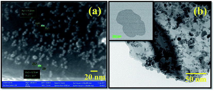 | ||
| Fig. 1 (a) High-magnification FESEM image of the as-synthesized PbS/MoS2 hybrid nanostructures for sample-S1. (b) Typical TEM micrographs of the as-synthesized PbS/MoS2 hybrid samples (sample-S1), showing a large number of well dispersed QDs attached on the MoS2 surface. Inset of (b) exhibits bare MoS2 nanosheets synthesized by the ion-intercalation method. | ||
The elemental composition and the nature of chemical bonding of PbS/MoS2 hybrid nanostructures were investigated by XPS and AES spectroscopy. Fig. 2(a) presents a selected area FESEM micrograph of sample S1, where the AES mapping has been acquired. Fig. 2(b), (c) and (d) show the individual elemental mapping images of Mo, S and Pb atoms, respectively, indicating the formation of a PbS/MoS2 hybrid. The combined AES mapping for all three elements (Mo, Pb and S), presented in Fig. 2(e), reveals their homogeneous distribution in the hybrid material. High-resolution AES spectra are presented in Fig. 2(f), showing the presence of Mo KLL, S KLL and Pb KLL transition lines in the sample. The atomic ratio (%) of the individual elements present in the hybrid is shown in the inset of Fig. 2(f). A slight Pb-richness in PbS/MoS2 hybrids is attributed to the presence of Pb on the surface due to its low surface diffusivity and the existence of S vacancies. The chemical bonding configuration of synthesized PbS/MoS2 hybrids has been studied by XPS spectroscopy using Al-Kα radiation of energy 1.4866 keV. High resolution XPS spectra of Mo, S and Pb core-level electrons are depicted in Fig. S3(a), (b) and (c), respectively (please see ESI†). The well-resolved characteristic doublets for Mo 3d (3d5/2 and 3d3/2), Pb 4f (4f7/2 and 4f5/2), and S 2p (2p3/2 and S 2p1/2) are in excellent agreement with their reported values, confirming the formation of Mo4+, Pb2+ and S2− states, respectively.27–29 The shift of binding energy peaks of S 2p (∼2.4 eV), Mo 3d (∼1 eV) and Pb 4f (∼1 eV) electrons with respect to their elemental values reveals the formation of Mo–S and Pb–S chemical bonds, supporting the formation of PbS decorated MoS2 nanosheets.
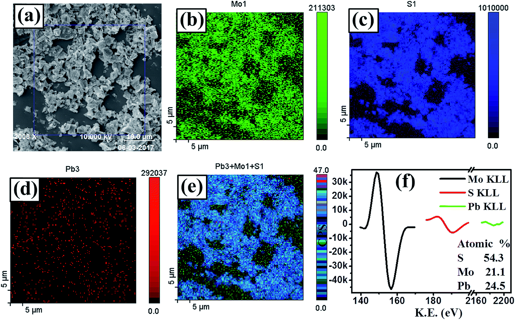 | ||
| Fig. 2 (a) SEM micrograph of the as-synthesized PbS/MoS2 hybrids (sample S1) used for Auger mapping. Auger electron spectroscopic images of the individual elementals showing the distribution of (b) Mo, (c) S and (d) Pb, along with (e) a combined elemental map. (f) Characteristic AES spectra of the elements present in sample-S1 to estimate their atomic percentage. | ||
XRD patterns of synthesized samples with different precursor ratios (S1–S4) are presented in Fig. 3(a). Duly indexed diffraction peaks confirm the coexistence of both PbS and MoS2 crystalline phases. However, the existence of multiple peaks suggests their polycrystalline nature. An intense peak at 14.1 degree for the (002) plane alongside four low intensity peaks at 33.1, 39.2, 57.5 and 61.2 degree is assigned to the (100), (103), (110) and (008) lattice planes of MoS2, respectively, indicating the formation of 2H semiconducting phase MoS2 (JCPDS file no. 89e2905) retaining crystalline quality and hexagonal symmetry, while diffraction peaks at 22.1, 26.2, 29.2, 44.3 and 50.5 degree representing the (110), (111), (200), (220) and (311) lattice planes of PbS, respectively, agreed well with the cubic PbS structure (JCPDS file no. 20e0596). The intensity ratio of the (002) plane of MoS2 to that of the (200) plane of PbS in the PbS/MoS2 hybrids reduces significantly with increasing Pb precursor concentration. The suppressed intensity is attributed to the increased size of PbS QDs, which wrap around the MoS2 surface, resulting in the attenuation of intensity. Room-temperature micro-Raman spectra of synthesized PbS decorated MoS2 hybrids for four different samples (S1–S4) are presented in Fig. 3(b) revealing the characteristic vibrational bands in the hybrids. The characteristic peaks of MoS2 at 379 and 404 cm−1 are ascribed to the in-plane (E12g band) and out-of-plane (A1g band) vibrational modes, respectively. The spacing between two characteristic Raman shifts is about ∼25 cm−1, which is in agreement with the previously reported results corroborating the formation of few layer MoS2 nanosheets.30 Slightly upshifted and broadened Raman vibrational bands compared to the bulk MoS2 indicate the existence of substantial local defects and disorder in hybrids. The observation reveals that the local symmetry in the hybrid structure is different from that of the bulk MoS2, though the crystal structure remains unaltered. The other vibrational peaks are attributed to the stretching of diatomic molecules of PbS QDs. The weak and wide peak at ∼138 cm−1 corresponds to the combination of longitudinal and transverse acoustic modes [LA (A) + TA (L)], whereas, the strong one, near ∼280 cm−1 is attributed to the surface phonons (SP). A broad peak near ∼448 cm−1 is ascribed to the 2LO (longitudinal optical) phonon modes in PbS QDs, whereas the one, near ∼520 cm−1 is the contribution from the Si substrate. The increase in the vibrational peak intensity ratio of PbS to MoS2 as a function of PbS QDs is clear evidence of a larger fraction of PbS coverage on the MoS2 surface. All the vibrational modes of PbS are upshifted and broadened in hybrid nanostructures, as compared to that of pristine PbS QDs reported in the literature.31,32 This is ascribed to the interaction between PbS and MoS2via electron transfer and the associated strain due to structural defects and disorder.
 | ||
| Fig. 3 (a) X-ray diffraction pattern and (b) Raman spectra of the samples revealing the simultaneous presence of 2D-MoS2 and 0D-PbS in hybrid nanostructures. | ||
Optical absorption spectra of as-prepared PbS/MoS2 hybrid samples (S1–S4), recorded in the visible and IR range are shown in Fig. 4(a) and (b), respectively. The absorption spectra in the visible regime (Fig. 4(a)) exhibit two characteristic peaks at 606 nm (∼2.04 eV) and 665 nm (∼1.86 eV), which are attributed to the excitonic band edge transitions from spin-degenerate valence bands to the conduction band near the K-point in the Brillouin zone of MoS2. The appearance of an intense broader absorption peak around ∼400 nm (∼3.16 eV) is assigned to the band nesting transition arising in a localized region between K and Γ-points in the band structure of MoS2 nanosheets.33 Notably, the optical absorption peak position in MoS2 nanosheets remains unaltered with the change of PbS QD size. The tunable absorption characteristics in the IR range from 1150 to 1350 nm with varying PbS QD size, shown in Fig. 4(b), are ascribed to the quantum confinement effect in PbS QDs. The near IR absorption peak, which is blue-shifted with decreasing PbS QD size, displays the size-tunable optical properties of PbS QDs. The results demonstrate the co-existence of optical signals from both 2D-MoS2 and 0D-PbS QDs, in the visible and IR region, respectively, making the 0D/2D hybrids attractive for the fabrication of two color-band (visible broadband and tunable IR) photodetectors.
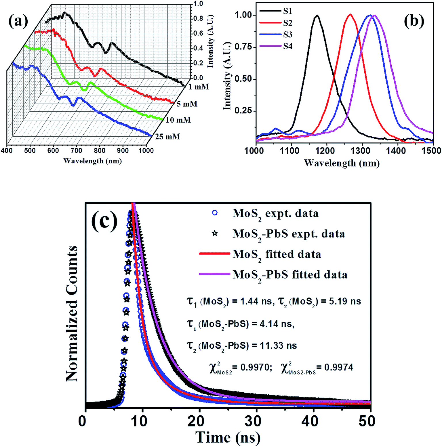 | ||
| Fig. 4 Optical absorption spectra of hybrid samples for the (a) visible and (b) infrared color region, illustrating 2D-MoS2 excitonic absorption features with the signature of the direct band edge transition and size dependent absorption features for 0D-PbS. (c) Time-resolved photoluminescence spectra of control MoS2 and PbS/MoS2 hybrids with the latter showing a higher carrier lifetime. Solid lines are fit to the experimental data using eqn (1). | ||
Photo-generated carrier lifetime in control MoS2 and PbS/MoS2 hybrid nanostructures was recorded at room temperature and the results are presented in Fig. 4(c). Experimental data for both the samples could be well fitted (solid lines) using the double exponent Marquardt–Levenberg algorithm, to compare and estimate the photogenerated carrier lifetime, given by,34
 | (1) |
3.2. Photodetection characteristics
The device response of synthesized PbS/MoS2 hybrid nanostructures has been studied by fabricating a flexible photodetector on a PET substrate. Digital photographs of the lithographically fabricated array of photodetectors are shown in Fig. 5(a). The details of substrate flexibility, transparency, device fabrication and indigenous testing set-up are presented in Fig. S4 (please see ESI†). The room temperature current–voltage (I–V) characteristics of the fabricated device for sample-S1 are illustrated in Fig. 5(b) under dark and illumination conditions. The symmetric I–V nature establishes the formation of a back-to-back junction between Au and PbS/MoS2 hybrid nanostructures. A significant increase in the current level upon monochromatic illumination (@ 514 nm, 0.15 mW cm−2) is due to the generation of photo-carriers leading to a high photo-to-dark current ratio of the order of ∼103 at a bias of −2 V. To study the photo-switching characteristics of the fabricated photodetector, the temporal photoresponse (I–t) under a pulsed illumination (@ λ = 514 nm) with various power densities at 2 V bias has been recorded and the results are presented in Fig. 5(c). The time-traces show a periodic and rapid alternate switching behavior of the current level upon pulsed illumination illustrating an excellent reproducibility, and a stable and reversible response of the photodetectors. An enhanced photo-current response has been observed with increasing the illumination intensity. The variation of photocurrent with incident optical power has been estimated and plotted in Fig. 5(d). The experimental data have been fitted using the power law IPh ∝ Pz, where the exponent “z” represents the rate of generation and recombination of electron–hole pairs leading to resultant photocurrent.36 The photocurrent (IPh) increases monotonically with incident optical power (P) suggesting that the generation rate of carriers is proportional to the absorbed photon flux. Therefore, the responsivity is constant throughout the measured power density regime, making the device attractive for practical applications.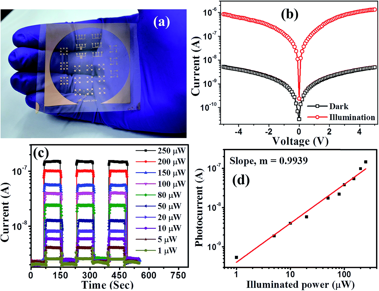 | ||
| Fig. 5 (a) Digital photographs of metal (Au) electrodes patterned on transparent and flexible PET substrates fabricated using the photolithography technique. (b) Typical current–voltage characteristics of the as-fabricated device under dark and illumination conditions. (c) Temporal current response of the device for various illumination intensities. (d) Photocurrent as a function of illumination power showing a linear dependency. | ||
The estimated spectral responsivity of the hybrid photodetector in the wavelength range from 400 to 1600 nm is presented in Fig. 6(a), for four different PbS QD sizes (S1–S4). The typical spectrum exhibits a broadband spectral response with the detection range extending to the IR region. The estimated peak response for the device with sample-S1 is found to be ∼398 mA W−1 for 480 nm and ∼543 mA W−1 for 1200 nm at 2 V. The responsivity value is almost constant in the visible wavelength range of 480 to 660 nm. On the other hand, the responsivity peak in the IR regime is ascribed to the optical transitions in PbS QDs under illumination. The photoresponse peak in the IR wavelength range exhibits a red shift with increasing PbS QD size, which could be useful to fabricate a wavelength selective IR detector. The responsivity spectra of fabricated detectors closely resemble the absorption characteristics of hybrid materials, indicating that the spectral selectivity is determined by the size induced bandgap of PbS QDs.
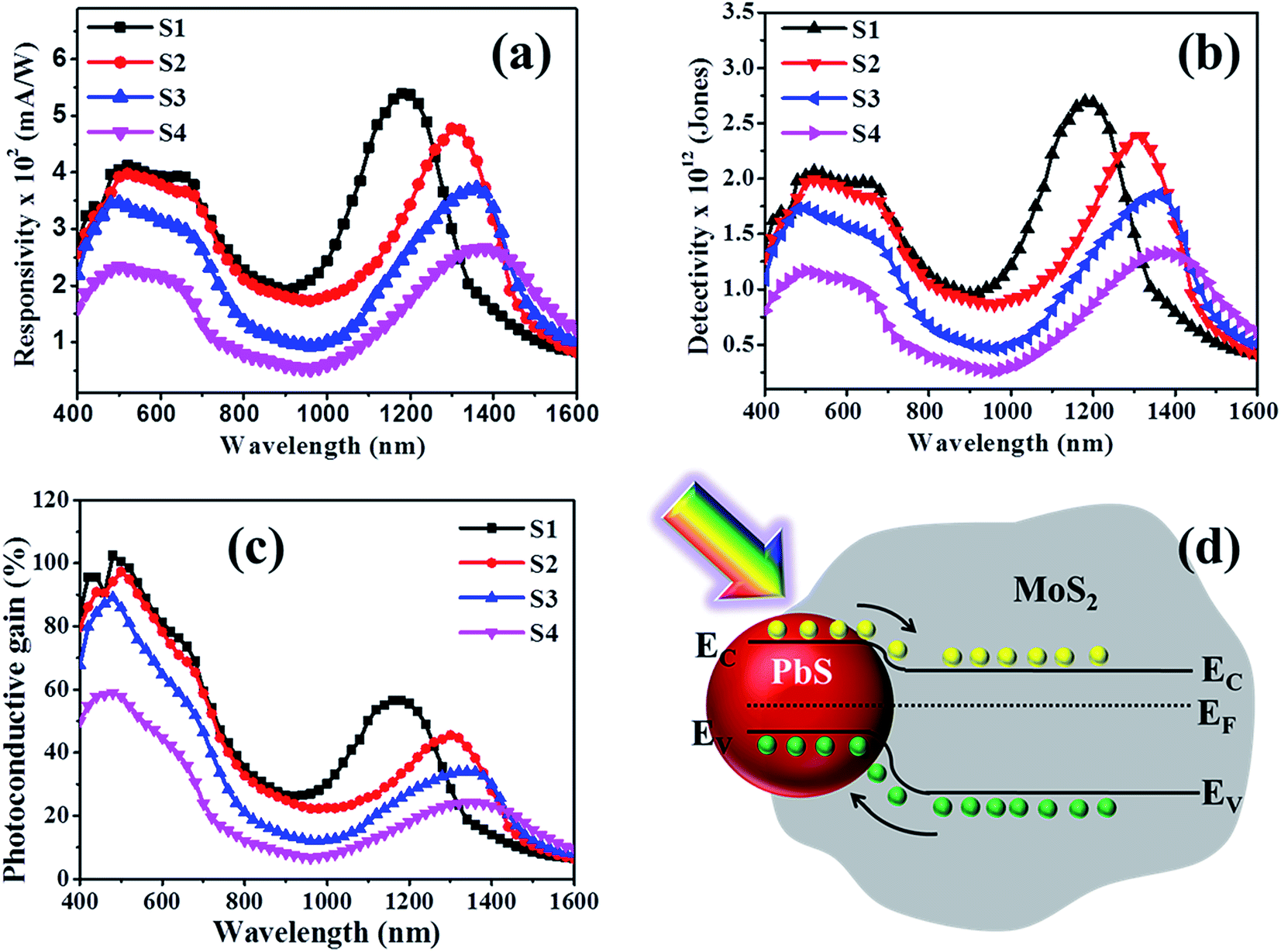 | ||
| Fig. 6 (a) Spectral responsivity, (b) detectivity and (c) photoconductive gain of the fabricated heterostructure for different samples, recorded at an applied bias of 2 V with 100 μW optical power. (d) Estimated band edge alignment of n-type MoS2 and p-type PbS showing the formation of a type-II heterojunction under equilibrium conditions. | ||
It is interesting to note that the hybrid device fabricated with the lowest QDs size (sample-S1) shows the highest responsivity, as shown in Fig. 6(a). The responsivity in both visible and IR regions decreases with increasing size of PbS QDs. This can be explained by the reduced carrier recombination lifetime in larger sized PbS QDs. The specific detectivity (D*) of a detector, the ability to differentiate the minimum optical signal power from the background noise, has been estimated as a function of wavelength over the 400–1600 nm range and is plotted in Fig. 6(b). The spectra show a peak detectivity of ∼2 × 10¹² Jones around 500 nm and ∼2.68 × 10¹² Jones around 1200 nm for 2 V bias, much higher than those of the standard Si or Ge based detectors.36,37 A comparison of the responsivity, detectivity and operation wavelength region of representative photodetectors fabricated using a similar type of colloidal QDs is provided in Table 1. It may be noted that our results are comparable or superior in terms of responsivity, detectivity and spectral wavelength coverage when compared with the all-solution processed colloidal QD based system as shown in Table 1.
| Sample description | Responsivity (A W−1) | Detectivity (Jones) | Operational spectral range | Ref. |
|---|---|---|---|---|
| PbS0.4Se0.6 colloidal quantum dot film | 0.05 | 4.11 × 10⁹ | 980 nm | 38 |
| PbS QDs/ZnO heterostructures | 2.73 | 2.39 × 10¹² | 532 nm | 39 |
| 0.42 | 3.65 × 10¹¹ | 808 nm | ||
| MoS2 nanocrystal film | 0.13 | — | 400–700 nm | 4 |
| HgTe QD capped with DDT ligands | 0.01 | — | 1620 nm | 40 |
| PbS colloidal QDs | 0.2 | 1012 | 1550 nm | 41 |
| HgSe colloidal QD film | 0.8 | 108 | 3000–8000 nm | 42 |
| PbS quantum dots with oleic acid capped | 0.2 | — | 1300–1500 nm | 43 |
| PbS QDs/MoS 2 hybrid heterostructure | 0.6 | 10 12 | 400–1600 nm | This work |
A combination of higher responsivity, lower dark current and lower noise levels leads to superior detectivity in 0D–2D hybrids. The detectivity is found to be significantly enhanced and the peak is blue shifted with the reduction of PbS QD size, similar to the responsivity behaviour. The photoconductive gain, defined as the ratio of collected carriers per incident photon per unit time, is related to the electronic transport and the carrier collection efficiency of a detector has been studied. The wavelength dependent photoconductive gain (GPh) is shown in Fig. 6(c). The figure illustrates that the smallest size PbS QD based device (S1) displays the highest gain, which is nearly 100% (1 electron collected per incident photon) at ∼500 nm. The relatively high photoconductive gain in the device originates from the synergistic effect of PbS/MoS2, where the MoS2 channel with high carrier mobility provides faster transfer of photogenerated electrons. Moreover, the longer carrier recombination lifetime in the 2D–0D hybrids is also beneficial for achieving a higher gain. At a higher bias, the photogenerated carriers are collected more efficiently, yielding a higher gain. However, for the highest PbS QD size (sample-S4), the photoresponse is found to be degraded. A combined effect of the attenuated illumination for higher PbS coverage, increased surface roughness scattering of carriers and reduced surface area contributes to the suppressed gain value. The improved photoresponse of the fabricated devices originates from the synergistic interaction of carriers between PbS QDs and MoS2 nanosheets. When p-type PbS QDs are in contact with n-type MoS2, surface electrons of MoS2 diffuse towards the PbS QDs until a built-in potential is formed at the interface and Fermi levels are in equilibrium. Consequently, the electron transfer reduces the energy level of the conduction band producing a type-II band alignment between n-MoS2 and p-PbS QDs. The resultant band diagram, under equilibrium conditions, is shown in Fig. 6(d). When the PbS/MoS2 hybrids are illuminated, the photogenerated electrons in PbS are easily transferred to the conduction band of MoS2, while holes move in the opposite direction. The enhanced photoresponse of the detector with applied bias is corroborated by the efficient collection of photocarriers at the electrodes in the presence of an electric field, resulting in a higher photocurrent (please see Fig. S5 in the ESI†). The most striking feature of the device is the combination of a high efficiency with a broadband spectral response in the visible region and tunable detection in the IR region.
The solution-based fabrication of hybrids is compatible with flexible platforms making it attractive for various applications. In order to study the effect of mechanical stress (bending) on the output characteristics, PbS/MoS2 hybrid devices have been fabricated on PET substrates. The dependence of the output current on the bending angle over various bending cycles has been studied and the results are presented in Fig. 7(a) and (b). The output current does not degrade with increasing bending angles up to 20 degree, as shown in Fig. 7(a). On the other hand, Fig. 7(b) displays an excellent stability of the current level over a fixed bending condition, which establishes the efficacy of the hybrid device for use as a flexible photodetector. This observation confirms the reproducibility and the repeatability of the device performance after recovering from a stressed condition. To the best of our knowledge, this is the first report on solution processed, IR absorbing QD decorated MoS2 devices, which can respond to two different colour bands ranging from 400–1600 nm and is compatible with flexible platforms.
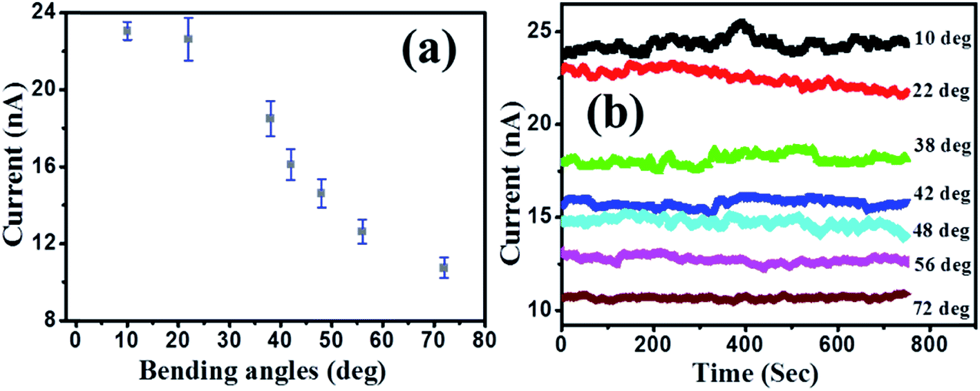 | ||
| Fig. 7 Dependence of the output dark current level on the (a) bending angle and (b) time for a fixed bending angle. | ||
4. Conclusions
We have demonstrated a novel and catalyst/stabilizer free, one-pot synthesis process of PbS/MoS2 hybrid nanostructures using a low temperature solvothermal method, which is promising for the fabrication of cost-effective, large area, two-color and infrared tunable wide-band photodetectors. The integration of 0D-PbS with 2D-MoS2 provides two significant advantages: (1) MoS2 acts as a substrate for nucleation and growth of PbS QDs and at the same time hinders their agglomeration. (2) The photo-excited electron–hole pairs in the hybrids could be efficiently separated in type-II heterostructures resulting in a higher photocurrent and gain. The device fabricated using the PbS QDs/MoS2 hybrid heterostructure demonstrates two colour detection with a broad spectral responsivity in the visible region and a tunable response in the IR region. The performance of the fabricated devices in the infrared region is significantly superior to that of their analogues with hybrid structures and even better than the performance of commercial Si-, Ge- and InGaAs-based devices. The solution processability of colloidal synthesis offered monolithic integration of devices on flexible substrates. The experimental findings suggest that the synergic 0D/2D hybrid heterostructure devices exhibit superior responsivity compared to solution processable devices achieved individually using PbS QDs or MoS2. This result could pave the way for the successful integration of 0D QDs in 2D materials toward novel and high performance next-generation photonic devices, compatible with standard CMOS technology as well as flexible platforms.Conflicts of interest
The authors declare no conflict of interest.Acknowledgements
The authors would like to acknowledge the partial financial support of the “NNETRA-SWI” project (Grant No. DST/NM/NNETRA/2018(G)) sponsored by Meity and DST, Govt. of India and the DST-CERI supported “ICF” Project at IIT Kharagpur (Grant No. DST/TM/CERI/C74(G)).References
- K. F. Mak, C. Lee, J. Hone, J. Shan and T. F. Heinz, Phys. Rev. Lett., 2010, 105, 136805 CrossRef.
- H. S. Lee, S. S. Baik, K. Lee, S. W. Min, P. J. Jeon, J. S. Kim, K. Choi, H. J. Choi, J. H. Kim and S. Im, ACS Nano, 2015, 9, 8312–8320 CrossRef CAS.
- A. Splendiani, L. Sun, Y. Zhang, T. Li, J. Kim, C. Y. Chim, G. Galli and F. Wang, Nano Lett., 2010, 10, 1271–1275 CrossRef CAS.
- S. Mukherjee, R. Maiti, A. Midya, S. Das and S. K. Ray, ACS Photonics, 2015, 2, 760–768 CrossRef CAS.
- A. Ebnonnasir, B. Narayanan, S. Kodambaka and C. V. Ciobanu, Appl. Phys. Lett., 2014, 105, 031603 CrossRef.
- K. Koåmider and J. Fernández-Rossier, Phys. Rev. B: Condens. Matter Mater. Phys., 2013, 87, 075451 CrossRef.
- D. Jariwala, T. J. Marks and M. C. Hersam, Nat. Mater., 2016, 16, 170 CrossRef.
- Y. Gong, J. Lin, X. Wang, G. Shi, S. Lei, Z. Lin, X. Zou, G. Ye, R. Vajtai, B. I. Yakobson, H. Terrones, M. Terrones, B. K. Tay, J. Lou, S. T. Pantelides, Z. Liu, W. Zhou and P. M. Ajayan, Nat. Mater., 2014, 13, 1135 CrossRef CAS.
- C. Li, X. Yan, X. Song, W. Bao, S. Ding, D. W. Zhang and P. Zhou, Nanotechnology, 2017, 28, 415201 CrossRef.
- Y. Chen, X. Wang, G. Wu, Z. Wang, H. Fang, T. Lin, S. Sun, H. Shen, W. Hu, J. Wang, J. Sun, X. Meng and J. Chu, Small, 2018, 14, 1703293 CrossRef.
- A. Midya, A. Ghorai, S. Mukherjee, R. Maiti and S. K. Ray, J. Mater. Chem. A, 2016, 4, 4534–4543 RSC.
- V. Dhyani and S. Das, Sci. Rep., 2017, 7, 44243 CrossRef.
- S. Mukherjee, S. Biswas, S. Das and S. K. Ray, Nanotechnology, 2017, 28, 135203 CrossRef CAS.
- R. Zhuo, Y. Wang, D. Wu, Z. Lou, Z. Shi, T. Xu, J. Xu, Y. Tiana and X. Li, J. Mater. Chem. C, 2018, 6, 299–303 RSC.
- A. Tayyebi, M. M. Tavakoli, M. Outokesh, A. Shafiekhani and A. A. Simchi, Ind. Eng. Chem. Res., 2015, 54, 7382–7392 CrossRef CAS.
- X. Song, Y. Zhang, H. Zhang, Y. Yu, M. Cao, Y. Che, H. Dai, J. Yang, X. Ding and J. Yao, Nanotechnology, 2017, 28, 145201 CrossRef.
- W. Feng, C. Qin, Y. Shen, Y. Li, W. Luo, H. An and Y. Feng, Sci. Rep., 2014, 4, 3777 CrossRef.
- V. R. Raja, D. R. Rosaline, A. Suganthi and M. Rajarajan, Solid State Sci., 2017, 67, 99–108 CrossRef CAS.
- S. Cho, Y. Jo, H. Woo, J. Kim, J. Kwak, H. Kim and H. Im, Applied Science and Convergence Technology, 2017, 26, 47–49 CrossRef.
- D. Kufer, I. Nikitskiy, T. Lasanta, G. Navickaite, F. H. L. Koppens and G. Konstantatos, Adv. Mater., 2015, 27, 176–180 CrossRef CAS.
- H. Zhao, D. Wang, M. Chaker and D. Ma, J. Phys. Chem. C, 2011, 115, 1620–1626 CrossRef CAS.
- M. Peng, X. Xie, H. Zheng, Y. Wang, Q. Zhuo, G. Yuan, W. Ma, M. Shao, Z. Wen and X. Sun, ACS Appl. Mater. Interfaces, 2018, 10, 43887–43895 CrossRef CAS.
- G. Flora, D. Gupta and A. Tiwari, Interdiscip. Toxicol., 2012, 5, 47–58 CAS.
- R. Saran and R. J. Curry, Nat. Photonics, 2016, 10, 81 CrossRef CAS.
- S. Mukherjee, S. Biswas, A. Ghorai, A. Midya, S. Das and S. K. Ray, J. Phys. Chem. C, 2018, 122, 12502–12511 CrossRef CAS.
- S. Acharya, D. D. Sarma, Y. Golan, S. Sengupta and K. Ariga, J. Am. Chem. Soc., 2009, 131, 11282–11283 CrossRef CAS.
- N. M. D. Brown, N. Cui and A. Mckinley, Appl. Surf. Sci., 1998, 134, 11–21 CrossRef CAS.
- N. P. Kondekar, M. G. Boebinger, E. V. Woods and M. T. McDowell, ACS Appl. Mater. Interfaces, 2017, 9, 32394–32404 CrossRef CAS.
- J. D. Patel, F. Mighri, A. Ajji and S. Elkoun, Mater. Sci. Appl., 2012, 3, 125–130 CAS.
- C. Lee, H. Yan, L. E. Brus, T. F. Heinz, J. Hone and S. Ryu, ACS Nano, 2010, 4, 2695–2700 CrossRef CAS.
- A. Milekhin, L. Sveshnikova, T. Duda, N. Surovtsev, S. Adichtchev, L. Ding and D. R. T. Zahn, J. Vac. Sci. Technol., B: Microelectron. Nanometer Struct.--Process., Meas., Phenom., 2010, 28, C5E22–C5E24 CrossRef CAS.
- A. V. Baranov, K. V. Bogdanov, E. V. Ushakova, S. A. Cherevkov, A. V. Fedorov and S. Tscharntke, Opt. Spectrosc., 2010, 109, 268–271 CrossRef CAS.
- S. H. Aleithan, M. Y. Livshits, S. Khadka, J. J. Rack, M. E. Kordesch and E. Stinaff, Phys. Rev. B, 2016, 94, 035445 CrossRef.
- S. Mukherjee, R. Maiti, A. K. Katiyar, S. Das and S. K. Ray, Sci. Rep., 2016, 6, 29016 CrossRef CAS.
- B. Martín-García, A. Polovitsyn, M. Prato and I. Moreels, J. Mater. Chem. C, 2015, 3, 7088–7095 Search PubMed.
- S. Mukherjee, K. Das, S. Das and S. K. Ray, ACS Photonics, 2018, 5, 4170–4178 CrossRef CAS.
- K. Das, S. Mukherjee, S. Manna, S. K. Ray and A. K. Raychaudhuri, Nanoscale, 2014, 6, 11232–11239 RSC.
- S. Muhammad, S. Yang, T. Song, H. Wang, Y. Wang, B. He, M. Dong, Y. Tang, Y. Song and B. Zou, RSC Adv., 2016, 6, 87730–87737 RSC.
- M. Peng, Y. Wang, Q. Shen, X. Xie, H. Zheng, W. Ma, Z. Wen and X. Sun, Sci. China Mater., 2019, 62, 225–235 CrossRef CAS.
- Z. Bingqing, M. Chen, S. V. Kershaw, A. L. Rogach, N. Zhao and H. K. Tsang, Conference on Lasers and Electro-Optics Pacific Rim (CLEO-PR), IEEE, 2017, pp. 1–3 Search PubMed.
- C. P. Jason, G. Konstantatos, K. W. Johnston, S. Hoogland, L. Levina and E. H. Sargent, Nat. Nanotechnol., 2009, 4, 40 CrossRef.
- L. Emmanuel, M. Scarafagio, P. Hease, B. Nadal, H. Aubin, X. Z. Xu, N. Lequeux, G. Patriarche, S. Ithurria and B. Dubertret, Nano Lett., 2016, 16, 1282–1286 CrossRef.
- M. Pawel, E. Georgitzikis, J. Maes, I. Vamvaka, F. Frazzica, J. V. Olmen, P. D. Moor, P. Heremans, Z. Hens and D. Cheyns, Sensors, 2017, 17, 2867 CrossRef.
Footnote |
| † Electronic supplementary information (ESI) available. See DOI: 10.1039/c9na00302a |
| This journal is © The Royal Society of Chemistry 2019 |