
 Open Access Article
 This Open Access Article is licensed under a Creative Commons Attribution-Non Commercial 3.0 Unported Licence
Physical mechanisms involved in the formation and operation of memory devices based on a monolayer of gold nanoparticle-polythiophene hybrid materials†
T.
Zhang
a,
D.
Guérin
a,
F.
Alibart
a,
D.
Troadec
a,
D.
Hourlier
a,
G.
Patriarche
 c,
A.
Yassin
b,
M.
Oçafrain
b,
P.
Blanchard
b,
J.
Roncali
bd,
D.
Vuillaume
a,
K.
Lmimouni
a and
S.
Lenfant
*a
c,
A.
Yassin
b,
M.
Oçafrain
b,
P.
Blanchard
b,
J.
Roncali
bd,
D.
Vuillaume
a,
K.
Lmimouni
a and
S.
Lenfant
*a
aInstitute of Electronics Microelectronics and Nanotechnology (IEMN), CNRS, University of Lille, Avenue Poincaré, F-59652 Villeneuve d'Ascq, France. E-mail: stephane.lenfant@iemn.univ-lille1.fr
bMOLTECH-Anjou, CNRS, University of Angers, 2 Bd Lavoisier, Angers, F-49045, France
cCentre for Nanoscience and Nanotechnology (C2N), CNRS, University of Paris-Saclay, Route de Nozay, Marcoussis, F-91460, France
dSupramolecular Organic and Organometallic Chemistry Center Babes, Bolyai University, 11 Arany Janos str, 400028 Cluj-Napoca, Romania
First published on 24th May 2019
Abstract
Understanding the physical and chemical mechanisms occurring during the forming process and operation of an organic resistive memory device is a requisite for better performance. Various mechanisms were suggested in vertically stacked memory structures, but the analysis remains indirect and needs destructive characterization (e.g. analysis of the cross-section to access the organic layers sandwiched between electrodes). Here, we report a study on a planar, monolayer thick, hybrid nanoparticle/molecule device (10 nm gold nanoparticles embedded in an electro-generated poly(2-thienyl-3,4-(ethylenedioxy)thiophene) layer), combining in situ physical (scanning electron microscopy, physicochemical thermogravimetry and mass spectroscopy, and Raman spectroscopy) and electrical (temperature dependent current–voltage) characterization on the same device. We demonstrate that the forming process causes an increase in the gold particle size, almost 4 times larger than the starting nanoparticles, and that the organic layer undergoes a significant chemical rearrangement from an sp3 to sp2 amorphous carbon material. Temperature dependent electrical characterization of this nonvolatile memory confirms that the charge transport mechanism in the device is consistent with a trap-filled space charge limited current in the off state, with the sp2 amorphous carbon material containing many electrically active defects.
1. Introduction
Organic resistive random-access memories (ORRAMs) are promising as fundamental elements for the development of electronic organic circuitries1,2 due to their various advantages, such as a simple and low cost fabrication process, light weight, mechanical flexibility and tunable materials properties. ORRAMs should present two non-volatile resistance states separated by at least 3 orders of magnitude.1,2 These resistance states can be read by measuring the current at a low voltage, and switched by applying a higher voltage sequence.We have recently demonstrated3 a hybrid memristive device based on a network of gold nanoparticles (GNPs) of 10 nm diameter connected by chains of a conjugated polymer. This molecule–GNP network was fabricated between two planar platinum electrodes a distance of 0.1 to 10 μm apart. After preparation of GNPs functionalized with 10-(2-(3,4-ethylenedioxythiophene)thiophen-3-sulfanyl)decane-1-thiol molecules, in situ electropolymerization of the thienyl-ethylenedioxythiophene moieties allowed the formation of a polymer–GNP monolayer4 (see the inset in Fig. 1b). As in many resistive memories,1 a forming process is mandatory before operation. The forming process consists of 3–4 voltage sweeps between 0 and 20 V at a sweep rate of ∼4 V s−1. Then, the electrical properties of these formed devices (Fig. 1) showed systematically (i) a negative differential resistance (NDR) behavior with a peak/valley ratio of up to 17 at a voltage of 6–7 V and (ii) a memory effect behavior with an on/off ratio in the 103 to 104 range. The retention time for both states was stable for at least 24 h, and the device stability was demonstrated for 800 cycles by switching between the two states.3 The devices showed no significant degradation in these 800 cycles between the ON and OFF states at a current ratio about 103. Then, reading pulses of up to 105 s were applied to measure the ON and OFF currents. The results showed good data retention without current drift in this memory.3 However, no clear physical mechanism was evidenced in previous studies.
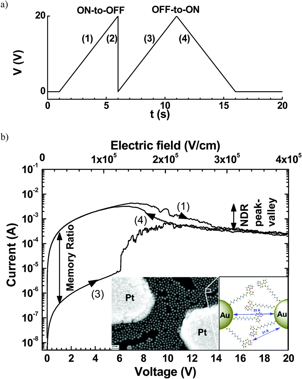 | ||
| Fig. 1 (a) Typical voltage sequence for the memory behavior and (b) the corresponding I–V curves for the ON-to-OFF and OFF-to-ON switches of a device after the forming process with a length L = 500 nm and width W = 1 mm. The current–voltage I–V traces are numbered according to the voltage sequences shown in (a). Inset, SEM image of a network of functionalized-GNP monolayer on a nanogap platinum electrodes (electrode spacing L = 200 nm and electrode width W = 100 nm); bar scale represents 30 nm; and schematic magnified view of a GNP interspace from ref. 3. Reprinted from ref. 3, copyright American Chemical Society 2017. | ||
Many studies on vertically stacked hybrid metal/organic–GNP/metal memories5–16 have proposed various mechanisms, such as (i) the formation of metallic filaments;13,14,16,17 (ii) electric field-induced charge transfer between organic materials and metallic nanoparticles;6,7 (iii) the inhibition of charge injection by the space-charge field of trapped charges inducing a space charge limited current (SCLC)8,12,15 and (iv) charge trapping/release in NP–organic composites6 or in NPs associated with tunneling through the organic material.10 However, these studies require destructive analysis, e.g. analysis of the cross-section to access the hybrid organic–NP layer between the metal electrodes for physicochemical studies.
In the present work, the advantage of a nanoscale monolayer thick planar structure placed between coplanar electrodes is that it makes it possible to characterize the physicochemical properties and electrical structure of the active material on the same device and also during operation for a better understanding of the mechanisms responsible for the forming process and resistive switching memory. Another advantage is the ability to prevent metal diffusion during top electrode deposition, which can also flaw the results in vertically stacked devices. Furthermore, the in situ electropolymerization process allows better control over the organization of the conjugated polymer GNP hybrid material and finally the active layer remains accessible and can be studied by several techniques during voltage cycles in order to better understand the physics of the operation mechanisms.
Here, we report on the mechanisms involved in the formation (forming process) and operation of devices based on an organic/GNP network with a monolayer thickness. For this purpose, different characterization studies have been carried out, namely (i) scanning (SEM) and transmission (STEM) electron microscopy of the morphological changes during the forming process and operation; (ii) evaluating the effects of thermal annealing on the morphology of the GNP network; (iii) analysis of the organic ligand material at high temperature and (iv) studying the temperature dependence of the charge transport behaviors in the two resistance states.
2. Materials and methods
Device fabrication
Electrochemical experiments were performed with a Modulab potentiostat from Solartron Analytical. The substrate with lithographed electrodes was hermetically fixed at the bottom of a 0.2 mL Teflon cell containing the electrolyte solution. The counter electrode was a platinum wire of 0.5 mm diameter and an Ag/AgCl electrode was used as a reference.
Electrical measurement setup
Electrical measurements were performed with an Agilent 4156C parameter analyzer in DC sweeping mode. We used a Carl Süss PM5 probe station in order to connect the Agilent 4156C and devices. All electrical measurements were performed under an inert atmosphere inside a dried nitrogen filled glove box (O2 < 1 ppm, H2O < 1 ppm).Thermogravimetry coupled with mass spectrometry analysis (TGA/MS)
Thermogravimetric analysis (TGA) (Netzsch STA449F3 Jupiter apparatus) coupled with quadrupole mass spectrometry (MS) (Aëolos QMS403D, 70 eV, electron impact) through a heated silica capillary system (0.220 mm internal diameter) has been used to monitor the thermal degradation of organic polymers. TGA provides information related to the changes in the sample mass during the annealing process, whereas mass spectrometry offers a method of identifying the evolved volatile species. Before each experiment, the TGA system was first evacuated and then flushed with ultrahigh purity helium before starting heating. The experiments were carried out under a dynamic inert gas atmosphere (helium: 99.999 purity) with a flow rate of 90 cm3 min−1. The samples were heated using a heating rate of 10°C min−1.Raman spectroscopy
Raman spectroscopy measurements were performed using a Horiba Jobin-Yvon LabRam®HR micro-Raman system combined with a 473 nm laser diode as the excitation source focused using a ×100 objective. The scattered light was collected using the same objective in the backscattering configuration, dispersed by a holographic grating of 1800 l mm−1 and detected using a CCD camera.Annealing of pTEDOT-C10-S-GNP monolayers
Freshly prepared pTEDOT-C10-S-GNP monolayers were subjected to thermal annealing under a nitrogen atmosphere (instrument: JetFirst 200 from JIPELEC). The annealing temperature (from 423 to 623 K with 50 K steps) was attained in 40 s from ambient temperature, and maintained for 120 s. After annealing, the samples were cooled to ambient temperature in 180 s.Scanning electron microscopy (SEM)
SEM observation was carried out using an MEB Ultra 55 purchased from Carl Zeiss or by Focused Ion Beam Strata DB 235 from FEI. The accelerating beam voltage was fixed at 10 kV and 5 kV respectively.Scanning transmission electron microscopy (STEM) analysis
Cross-section lamellae for the different samples were prepared with a focused ion beam (FIB) microscope (FEI STRATA DB 235). Milling steps were performed at 30 kV with the current decreasing from 20 nA to 30 pA and lamella thickness decreasing from 6 μm to less than 100 nm, followed by a final step at 5 kV and 30 pA to minimize amorphization. The transfer of the lamella samples to the TEM grid was done using a Kleindiek micromanipulator. The STEM observations of these cross-section lamellae were done on an FEI Titan Themis 200 microscope. This microscope is equipped with an aberration corrector on the probe (STEM mode) and a Super-X windowless EDX (4 quadrant SDD EDX detectors with a solid angle > 0.7 srad). The acceleration voltage was 200 kV and the probe current was about 50 pA with a half convergence angle of 17.6 mrad. The HAADF-STEM (high angle annular dark field) images were obtained on an annular dark field detector with a collection angle between 69 and 200 mrad.3. Results and discussion
Evolution of the morphology of the pTEDOT-C10-S-GNP monolayer during the forming process
After electropolymerization, a forming process is mandatory to form the formed-pTEDOT-C10-S-GNP monolayer and to “initialize” the device and observe the NDR and memory operation.3 It consists of 3–4 voltage sweeps from 0 to 20 V with a sweep rate of ∼4 V s−1 applied to the coplanar electrodes. SEM images of the same device before and after the forming process reveal that the sudden current increase at a voltage of about 6–7 V (see Fig. 4 in ref. 3) during the forming process is associated to an irreversible modification of the morphology of the pTEDOT-C10-S-GNP monolayer between the two electrodes (Fig. 2). The SEM image obtained after the forming process (Fig. 2b) exhibits brighter gold clusters between the two electrodes. These clusters can be associated to reorganization or aggregation, or fusion of the GNPs under the electric field (around 100 MV m−1) applied between the electrodes and/or due to the current density induced heating during the forming process. For comparison, the dissolution/nucleation of embedded metallic clusters of platinum inside a SiO2 layer was measured under a higher electrical field between 300 and 500 MV m−1.24 Here, the electric field is lower at 100 MV m−1 and can contribute to a lesser degree to the electro-migration of the GNPs into the polymer. To analyze these morphological modifications more precisely, STEM analysis (see methods) has been performed along the cross-sections of the monolayer (along the dashed line in Fig. 3a and b). The image recorded before the forming process (Fig. 3c) shows GNPs with ∼10 nm diameter, in agreement with the average value of 9.3 nm determined by the SEM analysis of the monolayer.3 The image obtained after the forming process (Fig. 3d) clearly shows larger gold clusters with a diameter of up to 40 nm. This STEM image of the clusters shows that the clusters have a regular round shape rather than a less regular shape expected for the aggregation of several GNPs. Moreover, the high-resolution STEM image clearly reveals the monocrystalline structure of this cluster (see Fig. SI-1†). These observations suggest that the clusters are formed by the melting of several GNPs during the forming process rather than by their aggregation.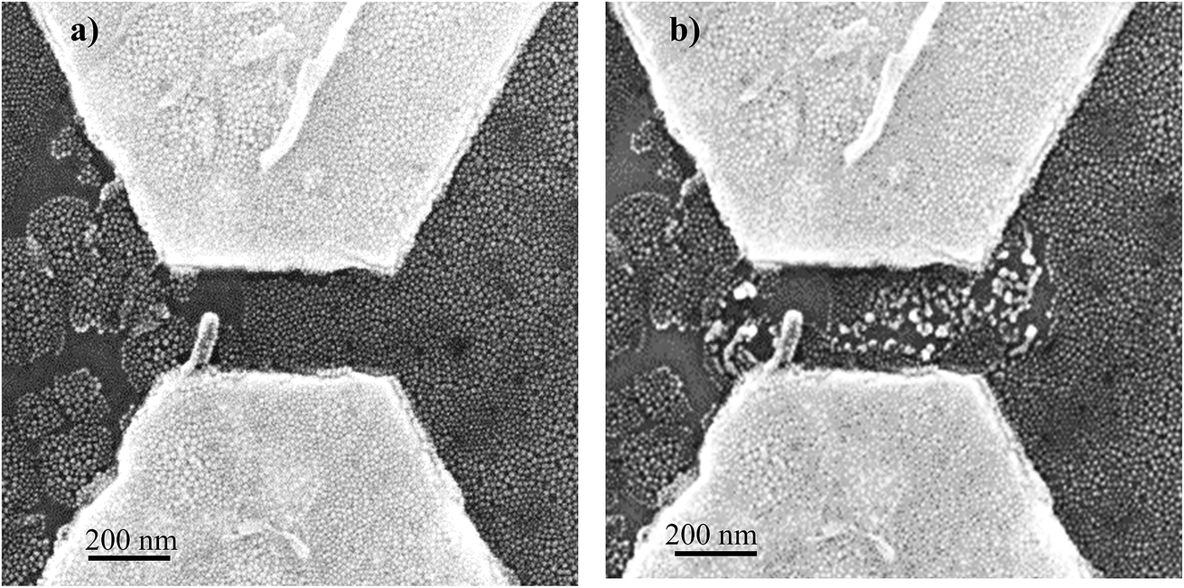 | ||
| Fig. 2 SEM images of a pTEDOT-C10-S-GNP monolayer in a 200 nm channel length (GNP size 10 nm) before (a) and after (b) the forming process consisting of 3–4 voltage sweeps from 0 to 20 V (corresponding to an electric field maximum of 100 MV m−1). | ||
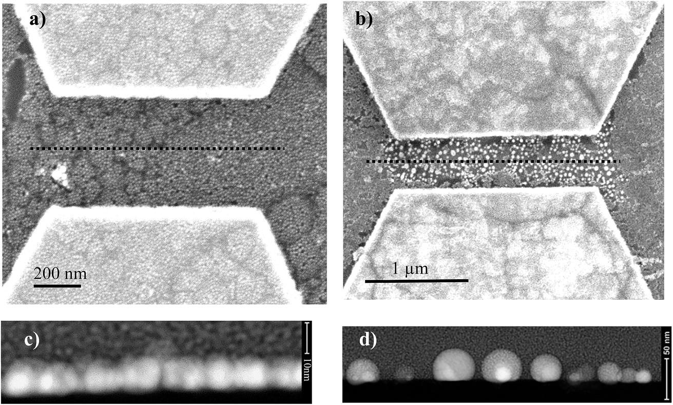 | ||
| Fig. 3 Top: (a) SEM image of the pTEDOT-C10-S-GNP monolayer (GNP size 10 nm). (b) SEM image of a formed-pTEDOT-C10-S-GNP monolayer after the forming process. Bottom: corresponding HAADF-STEM images of the cross section between the electrode along the dotted line in SEM images, (c) for device before the forming process (scale bar 10 nm) and (d) after the forming process (scale bar 50 nm). The two devices have the same channel length of 500 nm. | ||
Evolution of the morphology of the pTEDOT-C10-S-GNP monolayer during thermal annealing
To understand the physical origin of the cluster formation and to estimate the temperature attained in the device during the forming process, pTEDOT-C10-S-GNP monolayers are annealed at different temperatures from 423 to 623 K with 50 K steps (see methods) and imaged by SEM (Fig. 4). At lower temperatures (423 and 473 K), the GNPs present an average diameter of ∼10 nm, in agreement with the average value of 9.3 nm determined by SEM and STEM analyses of the as-fabricated samples.3 At 523 K, some clusters with a characteristic size between 20 and 40 nm appear in the monolayer. At higher temperatures, 573 K and 623 K, the number of these clusters increases dramatically. Finally, at 623 K, the majority of the GNPs melt to form these clusters.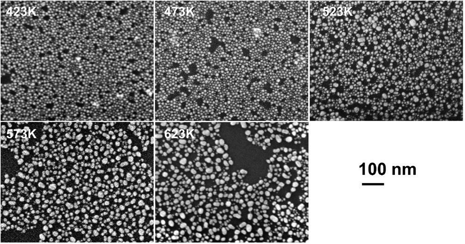 | ||
| Fig. 4 SEM images of a pTEDOT-C10-S-GNP monolayer after thermal annealing at different temperatures from 423 to 623 K with 50 K steps. Images were acquired in the gap electrode. | ||
The round shape and the size of the clusters formed by thermal annealing at 623 K are maintained after the forming process (Fig. 2b and 3b). This similarity suggests that during the forming process, the formation of clusters is caused by a local current-induced increase of the temperature in the monolayer (Joule effect).
We observe the beginning of the melting of GNPs at ∼523 K (Fig. 4) while the melting point (mp) for bulk gold is 1337 K.25 According to Buffat's thermodynamic model,26,27 which correlates the mp of naked metal nanoparticles to their mean diameter, the mp for 9.3 nm diameter GNPs is predicted to be 1273 K. On the other hand, this value is drastically reduced when the GNP surface is coated with molecules28 or silica.29 These coating materials increase the surface energy value of the solid phase of the GNPs and reduce the mp, in agreement with Buffat's model. For example, Miyake et al.28 have investigated the effect of thermal annealing on 2D superlattices (hexagonal packing) of GNPs coated with dodecane or octadecane-thiol. After thermal annealing at 423 K, the diameter of the dodecane coated GNPs increases from 1.5 ± 0.2 nm to 3.4 ± 0.3 nm. For coated GNPs with ∼10 nm diameter, these authors estimate a mp of around 535 K which is close to the threshold temperature of 523 K observed in our experiments. Thus, we suggest that during the forming process a local temperature of at least 523 K is attained in the pTEDOT-C10-S-GNP monolayer leading to the formation of clusters by the melting of the 10 nm diameter GNPs.
It was shown that in metal/oxide/metal coplanar structures for memory or memristive applications such as Ag/SiO2/Pt,30 W/SiO2/Ag24 or Pt/Ag nanoclusters in SiO2/Pt system,31 the formation of metallic clusters may be caused by metal displacement or migration along the direction of the electric field between the metallic electrodes. However, to the best of our knowledge, no previous study mentioning the formation of clusters in organic bistable memories by a thermal effect has been reported so far.
Thermogravimetry coupled with mass spectrometry analysis (TGA/MS) and Raman spectroscopy
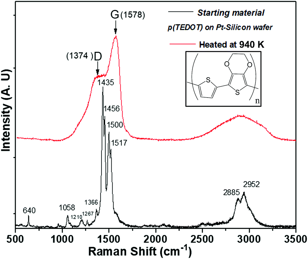
Since high temperatures (higher than 523 K) can be attained in the samples during the forming process, it was important to assess the thermal stability of organic ligands. Simultaneous thermogravimetry (TG) coupled with mass spectrometry (MS) was used to elucidate the thermal degradation/modification of organics. Two different organic compounds have been tested: (i) a conjugated polymer namely p(TEDOT) and (ii) 2 nm diameter GNPs functionalized with HS-C10-TEDOT (insets in Fig. 5). GNPs with 2 nm diameter instead of 10 nm have been chosen in order to improve the percentage in mass of the organic material, and therefore the sensitivity of analytical measurements (TG and MS). Indeed, with a surface density of 4.0 molecules per nm2 determined by XPS,3 the percentage in mass of organic material for nanoparticles of 2 nm and 10 nm diameter is estimated to be around 29% and 8%, respectively.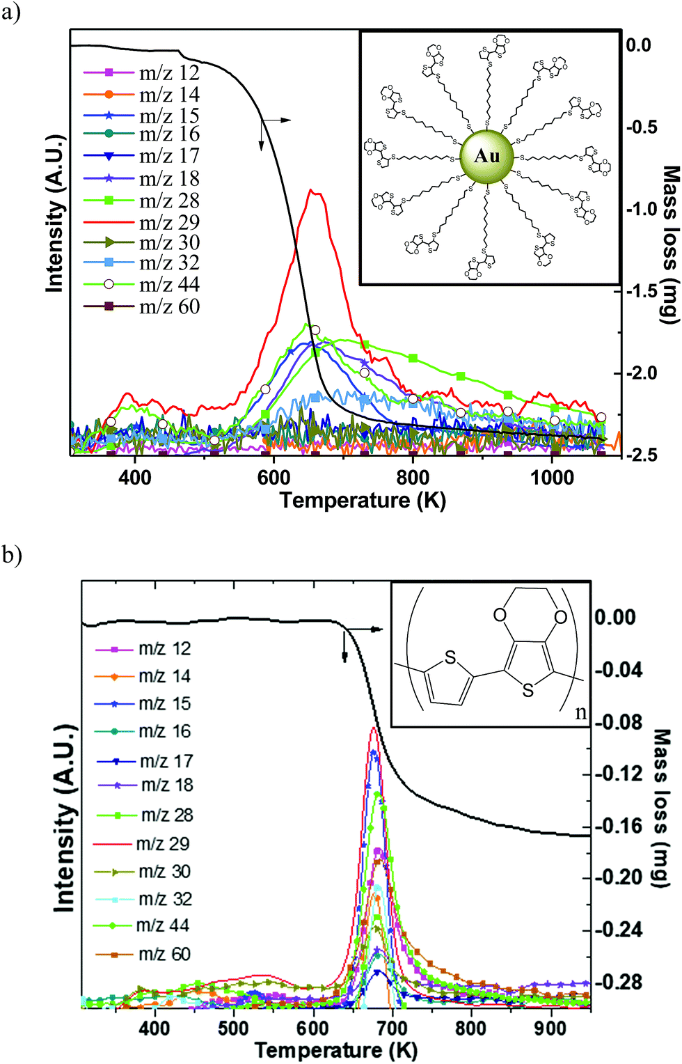 | ||
| Fig. 5 Thermogravimetry analysis (TGA) coupled with mass spectrometry (MS) of (a) a brittle-porous sample of TEDOT-C10-S-GNPs with 2 nm diameter GNPs (scheme in the inset) (b) the thin p(TEDOT) film on Si/Pt substrate (p(TEDOT) structure in the inset). | ||
Fig. 5a and b show the TG/MS traces measured for the 2 nm diameter GNPs functionalized with the HS-C10-TEDOT ligand (powder was placed directly into a crucible), and for a thin film of p(TEDOT) (thickness of around 100 μm) on a Si/Pt substrate prepared by electropolymerization of TEDOT monomers in a solution unit.32 For TG/MS and Raman analyses of the p(TEDOT) film, we use the TEDOT molecule without the alkylthiol moiety as the reference in order to (i) maximize the thickness of the electropolymerized film by removing the electrically resistive part of the molecule and (ii) avoid the oxidation of the thiol group of the molecule during the electropolymerization. We assume that the conclusions of these analyses on p(TEDOT) films are valid for the p(S-C10-TEDOT) systems.
The decomposition of the TEDOT moiety in TEDOT-C10-S-GNP starts occurring much earlier than that of p(TEDOT) which requires a high temperature of about 620 K (Fig. 5b). Both organic-based samples display one major mass loss, between 450 and 720 K for TEDOT-C10-S-GNP and between 620 K and 720 K for p(TEDOT), involving the release of volatile species corresponding to numerous different ions detected by mass spectrometry. The mass spectrometry spectrum is shown only to emphasize the relationship between the mass losses recorded by TGA and the released gaseous species. As the quantity of organics is much lower than the one of gold particles and/or the silicon substrate, the decomposition of organic ligands does not produce a strong enough mass-spectrometry signal for the assignment of the series of ions (m/z) to establish a clear-cut fragmentation pathway of evolved volatile molecules. Further work is clearly needed to clarify the decomposition mechanism of these materials.
As with many organic compounds, when TEDOT-C10-S-GNPs and p(TEDOT) are heated, the structural modification leads not only to volatile molecules, but also to a black residue called free carbon. TEDOT-C10-S-GNPs left a porous brittle black residue unsuitable for further analysis. However, the residue left on the silicon substrate from p(TEDOT), which was easier to handle, has been characterized by Raman spectroscopy. Fig. 6 depicts the Raman spectra recorded from the polymer p(TEDOT) deposited on the Pt/Silicon wafer and the one thermally treated in helium at 940 K. In agreement with the literature,33–35 the main Raman bands of the TEDOT moiety are observed in the spectrum and are listed in Table 1. As expected, the heated TEDOT-C10-S-GNP-based material exhibited the two characteristic broad C sp2-bands (band D at 1374 cm−1 and band G at 1578 cm−1) of amorphous free carbon.
 | ||
| Fig. 6 Raman spectroscopy acquired from p(TEDOT) polymer deposited on Pt-silicon substrate before and after a thermal annealing in helium at 940 K. | ||
| Wave number (cm−1) | Assignment of Raman bands |
|---|---|
| 640 | Oxyethylene ring deformation |
| 1058 | C–O–C deformation |
| 1210 | Stretching 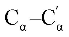 (inter-ring) (inter-ring) |
| 1267 | Stretching  (inter-ring), Cβ–H bending (inter-ring), Cβ–H bending |
| 1366 | Stretching Cβ–Cβ intra-ring |
| 1435 | Symmetric stretching Cα![[double bond, length as m-dash]](https://www.rsc.org/images/entities/char_e001.gif) Cβ(–O) Cβ(–O) |
| 1456 | Symmetric stretching CαCβ(–H) |
| 1500 | Asymmetric stretching CC |
| 1517 | Asymmetric stretching CC |
| 2885 | CH2 stretching |
| 2952 | CH2 stretching |
Temperature-dependent charge transport mechanisms
After the forming process, the device is set to the ON state by applying a double voltage sweep (amplitude from 0 to 20 and 20 to 0 V at 4V s−1), and in the OFF state by applying a single voltage sweep (0 to 20 V at 4V s−1) followed by an abrupt return to 0 V (Fig. 1a).3 The charge transport properties of both states are characterized in the 80–300 K temperature range by measuring the ON and OFF current at a fixed reading bias of 1 V (Fig. 7). The Arrhenius plots for the ON and OFF currents show that the OFF current is weakly thermally activated with an activation energy of Ea = 51 meV above a threshold temperature of ∼170 K, and not thermally activated below this temperature. The current in the ON state is not thermally activated in the 80 to 300 K temperature range. This behavior is similar to that previously reported for memory devices based on TiO2 nanoparticles embedded in poly(9-vinylcarbazole) films with no activation energy for the ON state, and an activation energy of ∼66 meV for the OFF state at temperatures above 150 K.36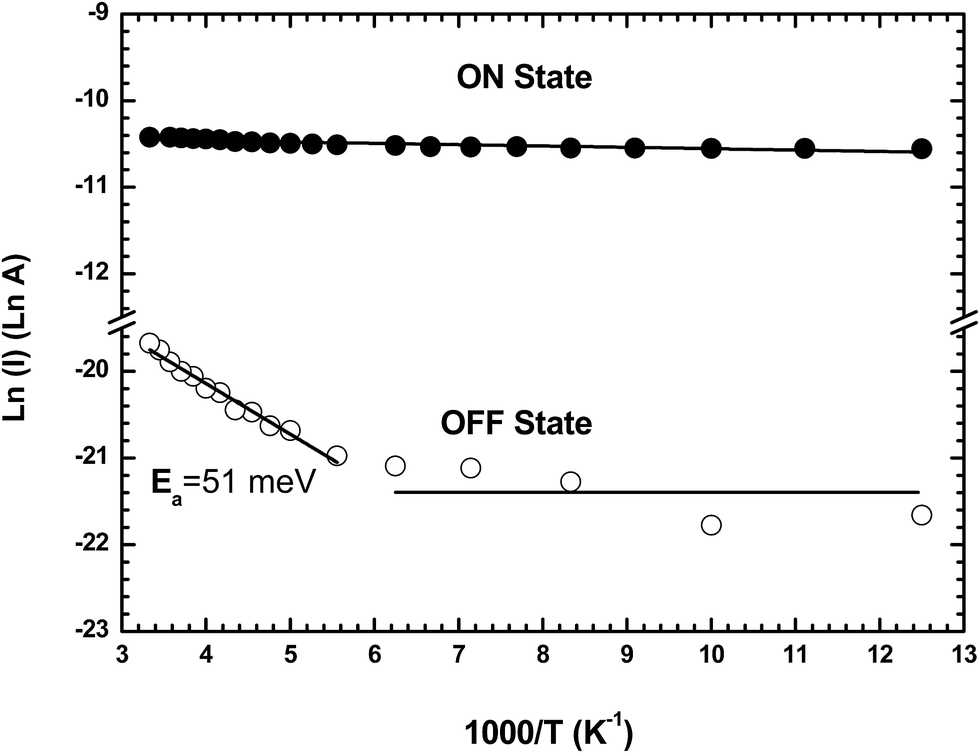 | ||
| Fig. 7 Arrhenius plot of the current in the ON and OFF states in the temperature range from 80 to 300 K read at 1 V for a formed-pTEDOT-C10-S-GNP monolayer in a 500 nm × 1000 μm channel device. | ||
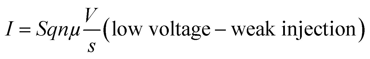
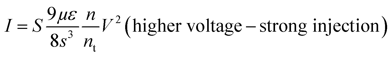
Several models of the charge transport mechanism could be suggested to explain the current–voltage (I–V) characteristics measured on the memory device, such as space charge limited current (SCLC), variable range hopping and thermionic emission limited conduction.37I–V characteristics measured at 300 K in the OFF state (Fig. 8) are not consistent with the variable range hopping or thermionic emission limited conduction models (for details see the ESI†). In the case of the SCLC model, the I–V curve in the log–log scale shows two distinct regions with different I–V relationships (Fig. 8). From low voltages (<1 V) in the OFF state the current increases linearly with the bias voltage (region 1). For voltages between 1 V and 10 V (region 2), the current exhibits a voltage square dependence. In the ON state, a linear relationship is observed from voltages up to 7 V. The I–V characteristics in the OFF state are well explained by a SCLC mechanism according to the following two equations for low and high voltage regions respectively (from ref. 37):
 | (1) |
 | (2) |
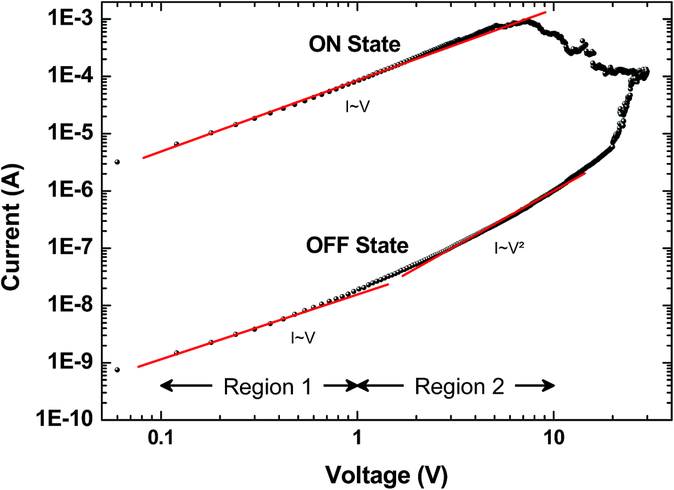 | ||
| Fig. 8 Typical current I versus voltage V curves (log–log scale) for the memory behavior measured on a formed-pTEDOT-C10-S-GNP device with a 1 μm gap length. Dots correspond to experimental data and red lines to the fitting adjustments before switching regions; i.e. in region 1 (0.1 to 1 V) and region 2 (1 to 10 V) for the OFF state, and from 0.1 to 7 V for the ON state. From these adjustments at low and high voltage and with eqn (1) and eqn (2), we estimate the density of trapped charge nt ∼ 1.6 × 1014 cm−3. | ||
Physical interpretation of the mechanism in the device
Cho et al.36 observed that the ON state of memory devices based on TiO2 nanoparticles embedded in poly(9-vinylcarbazole) films followed an ohmic behavior and also observed a negligible temperature dependence of the current (i.e. no thermal activation). They concluded that the current in the ON state is mainly due to charge tunneling between filament conducting paths. Here the same features are observed. Thus, it is likely that the ON state of the device in this study corresponds to conduction through conducting pathways formed during the “forming process”. Based on the above SEM, STEM and Raman measurements, we conclude that the nature of these conducting paths is based on the hybrid material composed of amorphous sp2 carbon and gold clusters.In the OFF state, we observed a weak thermal activation above 170 K and the I–V characteristics are well explained by a trap-filled SCLC current model. Lin et al.12 also observed SCLC behavior in the OFF state for devices composed of a layer of polystyrene mixed with GNPs of 2–5 nm diameter sandwiched between two aluminum electrodes. As discussed in our previous work,3 a charge carrier trapping/release mechanism from traps can explain these characteristics: (i) the ohmic behavior in the ON state corresponds to transport of free carriers in the hybrid material (see above); and (ii) the SCLC transport in the OFF state corresponds to injection limited transport when charge carriers are trapped in defects (traps) in the materials.
The physical mechanisms proposed here are close to that described by Simmons and Verderber in MIM structures in the 1960s, involving charge trapping/release and space charge field inhibition of injection.38 The nature of the traps involved in the mechanism was generally associated to the NPs present in the hybrid organic/gold nanoparticle memories.3,7,8,10,12 In the device presented here, after the forming process the resulting material is composed of gold clusters and amorphous sp2 carbon. The gold clusters and amorphous sp2 carbon can act as trapping centers. sp2 carbon was suggested to be the trapping centers in hybrid poly(N-vinylcarbazole)-graphene nonvolatile memory devices.39 Regarding the influence of the organic matrix on the electrical properties, the forming process induces an annealing of the organic matrix leading to the formation of amorphous sp2 carbon. Moreover, we assume that switching and cluster formation can occur for other organic polymers incorporated into the device, but with some variation in the voltage values in the memory behavior due to the difference of gold diffusivity or sp2 carbon formation for example.
4. Conclusions
Through the course of this study, we followed the physical mechanism involved in the forming process and operations of a hybrid memristive device based on a network of GNPs embedded in an electrogenerated pTEDOT matrix. The forming process leads to morphological modifications of the hybrid 2D monolayer film. Larger gold clusters of about 40 nm in diameter appear between the electrodes, similar to those obtained after thermal annealing of the GNP network at ∼523 K. TG/MS and Raman analysis show evidence of changes in structural organic polymers. The resulting hybrid material, made of amorphous sp2 carbon and gold clusters, is assumed to contain electrical traps, which can explain the voltage and temperature dependence of charge carrier transport in this device.Conflicts of interest
There are no conflicts to declare.Acknowledgements
This work has been financially supported by EU FET project no. 318597 “SYMONE”, the ANR agency, project no. ANR 12 BS03 010 01 “SYNAPTOR” and the French RENATECH network. The authors thank the clean room staff of the IEMN for the assistance and help with device fabrication.References
- F. Pan, S. Gao, C. Chen, C. Song and F. Zeng, Recent progress in resistive random access memories: materials, switching mechanisms, and performance, Mater. Sci. Eng., R, 2014, 83, 1–59 CrossRef.
- S. Gao, X. Yi, J. Shang, G. Liu and R.-W. Li, Organic and hybrid resistive switching materials and devices, Chem. Soc. Rev., 2019, 48, 1531–1565 RSC.
- T. Zhang, D. Guérin, F. Alibart, D. Vuillaume, K. Lmimouni, S. Lenfant, A. Yassin, M. Oçafrain, P. Blanchard and J. Roncali, Negative Differential Resistance, Memory, and Reconfigurable Logic Functions Based on Monolayer Devices Derived from Gold Nanoparticles Functionalized with Electropolymerizable TEDOT Units, J. Phys. Chem. C, 2017, 121(18), 10131–10139 CrossRef CAS.
- A. Yassin, M. Ocafrain, P. Blanchard, R. Mallet and J. Roncali, Synthesis of Hybrid Electroactive Materials by Low-Potential Electropolymerization of Gold Nanoparticles Capped with Tailored EDOT-Thiophene Precursor Units, ChemElectroChem, 2014, 1(8), 1312–1318 CrossRef CAS.
- L. Ma, J. Liu and Y. Yang, Organic electrical bistable devices and rewritable memory cells, Appl. Phys. Lett., 2002, 80(16), 2997–2999 CrossRef CAS.
- R. J. Tseng, J. Huang, J. Ouyang, R. B. Kaner and Y. Yang, Polyaniline nanofiber/gold nanoparticle nonvolatile memory, Nano Lett., 2005, 5(6), 1077–1080 CrossRef CAS PubMed.
- A. Prakash, J. Ouyang, J.-L. Lin and Y. Yang, Polymer memory device based on conjugated polymer and gold nanoparticles, J. Appl. Phys., 2006, 100(5), 054309 CrossRef.
- L. D. Bozano, B. W. Kean, M. Beinhoff, K. R. Carter and J. C. Scott, Adv. Funct. Mater., 2005, 15, 1933 CrossRef CAS.
- J. Li, A. Tang, X. Li, Y. Cao, M. Wang, Y. Ning, L. Lv, Q. Lu, Y. Lu, Y. Hu, Y. Hou and F. Teng, Negative differential resistance and carrier transport of electrically bistable devices based on poly(N-vinylcarbazole)-silver sulfide composites, Nanoscale Res. Lett., 2014, 9, 128 CrossRef PubMed.
- D. I. Son, D. H. Park, J. Bin Kim, J. W. Choi, T. W. Kim, B. Angadi, Y. Yi and W. K. Choi, Bistable Organic Memory Device with Gold Nanoparticles Embedded in a Conducting Poly(N-vinylcarbazole) Colloids Hybrid, J. Phys. Chem. C, 2011, 115(5), 2341–2348 CrossRef CAS.
- J. Y. Ouyang, Materials effects on the electrode-sensitive bipolar resistive switches of polymer: gold nanoparticle memory devices, Org. Electron., 2013, 14(6), 1458–1466 CrossRef CAS.
- H.-T. Lin, Z. Pei and Y.-J. Chan, Carrier transport mechanism in a nanoparticle-incorporated organic bistable memory device, IEEE Electron Device Lett., 2007, 28(7), 569–571 CAS.
- G. Casula, P. Cosseddu, Y. Busby, J.-J. Pireaux, M. Rosowski, B. T. Szczesna, K. Soliwoda, G. Celichowski, J. Grobelny, J. Novak, R. Banerjee, F. Schreiber and A. Bonfiglio, Air-stable, non-volatile resistive memory based on hybrid organic/inorganic nanocomposites, Org. Electron., 2015, 18, 17–23 CrossRef CAS.
- D. Tondelier, K. Lmimouni, D. Vuillaume, C. Fery and G. Haas, Metal/organic/metal bistable memory devices, Appl. Phys. Lett., 2004, 85(23), 5763–5765 CrossRef CAS.
- L. D. Bozano, B. W. Kean, V. R. Deline, J. R. Salem and J. C. Scott, Mechanism for bistability in organic memory elements, Appl. Phys. Lett., 2004, 84(4), 607–609 CrossRef CAS.
- Y. Busby, N. Crespo-Monteiro, M. Girleanu, M. Brinkmann, O. Ersen and J.-J. Pireaux, 3D imaging of filaments in organic resistive memory devices, Org. Electron., 2015, 16, 40–45 CrossRef CAS.
- G. Casula, Y. Busby, A. Franquet, V. Spampinato, L. Houssiau, A. Bonfiglio and P. Cosseddu, A flexible organic memory device with a clearly disclosed resistive switching mechanism, Org. Electron., 2019, 64, 209–215 CrossRef CAS.
- M. Ocafrain, T. K. Tran, P. Blanchard, S. Lenfant, S. Godey, D. Vuillaume and J. Roncali, Electropolymerized self-assembled monolayers of a 3,4-ethylenedioxythiophene-thiophene hybrid system, Adv. Funct. Mater., 2008, 18(15), 2163–2171 CrossRef CAS.
- F. Wang, C. He, M.-Y. Han, J. H. Wu and G. Q. Xu, Chemical controlled reversible gold nanoparticles dissolution and reconstruction at room-temperature, Chem. Commun., 2012, 48(49), 6136–6138 RSC.
- C. Shen, C. Hui, T. Yang, C. Xiao, J. Tian, L. Bao, S. Chen, H. Ding and H. Gao, Monodisperse Noble-Metal Nanoparticles and Their Surface Enhanced Raman Scattering Properties, Chem. Mater., 2008, 20(22), 6939–6944 CrossRef CAS.
- H. Hiramatsu and F. E. Osterloh, A simple large-scale synthesis of nearly monodisperse gold and silver nanoparticles with adjustable sizes and with exchangeable surfactants, Chem. Mater., 2004, 16(13), 2509–2511 CrossRef CAS.
- Y. Viero, G. Copie, D. Guerin, C. Krzeminski, D. Viiillaume, S. Lenfant and F. Cleri, High Conductance Ratio in Molecular Optical Switching of Functionalized Nanoparticle Self-Assembled Nanodevices, J. Phys. Chem. C, 2015, 119(36), 21173–21183 CrossRef CAS.
- V. Santhanam, J. Liu, R. Agarwal and R. P. Andres, Self-assembly of uniform monolayer arrays of nanoparticles, Langmuir, 2003, 19(19), 7881–7887 CrossRef CAS.
- Y. Yang, P. Gao, L. Li, X. Pan, S. Tappertzhofen, S. Choi, R. Waser, I. Valov and W. D. Lu, Electrochemical dynamics of nanoscale metallic inclusions in dielectrics, Nat. Commun., 2014, 5, 4232 CrossRef CAS PubMed.
- D. R. Lyde, Handbook of Chemistry and Physics, CRC Press, Boca Raton, 74th edn, 1993, pp. 1993–1994 Search PubMed.
- P. Buffat and J. P. Borel, Size effect on melting temperature of gold particles, Phys. Rev. A: At., Mol., Opt. Phys., 1976, 13(6), 2287–2298 CrossRef CAS.
- L. J. Lewis, P. Jensen and J. L. Barrat, Melting, freezing, and coalescence of gold nanoclusters, Phys. Rev. B: Condens. Matter Mater. Phys., 1997, 56(4), 2248–2257 CrossRef CAS.
- T. Shimizu, T. Teranishi, S. Hasegawa and M. Miyake, Size evolution of alkanethiol-protected gold nanoparticles by heat treatment in the solid state, J. Phys. Chem. B, 2003, 107(12), 2719–2724 CrossRef CAS.
- K. Dick, T. Dhanasekaran, Z. Zhang and D. Meisel, Size-Dependent Melting of Silica-Encapsulated Gold Nanoparticles, J. Am. Chem. Soc., 2002, 124(10), 2312–2317 CrossRef CAS PubMed.
- Y. Yang, P. Gao, S. Gaba, T. Chang, X. Pan and W. Lu, Observation of conducting filament growth in nanoscale resistive memories, Nat. Commun., 2012, 3, 732 CrossRef PubMed.
- Y. Yang, B. Chen and W. D. Lu, Memristive Physically Evolving Networks Enabling the Emulation of Heterosynaptic Plasticity, Adv. Mater., 2015, 27(47), 7720–7727 CrossRef CAS PubMed.
- M. Turbiez, P. Frère, P. Blanchard and J. Roncali, Mixed π-conjugated oligomers of thiophene and 3,4-ethylenedioxythiophene (EDOT), Tetrahedron Lett., 2000, 41(29), 5521–5525 CrossRef CAS.
- P. Larkin, Infrared and Raman Spectroscopy, Elsevier, Oxford, 2011 Search PubMed.
- J. L. Duvail, P. Retho, S. Garreau, G. Louarn, C. Godon and S. Demoustier-Champagne, Transport and vibrational properties of poly(3,4-ethylenedioxythiophene) nanofibers, Synth. Met., 2002, 131(1–3), 123–128 CrossRef CAS.
- S. Garreau, J. L. Duvail and G. Louarn, Spectroelectrochemical studies of poly(3,4-ethylenedioxythiophene) in aqueous medium, Synth. Met., 2001, 125(3), 325–329 CrossRef.
- B. Cho, T. W. Kim, M. Choe, G. Wang, S. Song and T. Lee, Unipolar nonvolatile memory devices with composites of poly(9-vinylcarbazole) and titanium dioxide nanoparticles, Org. Electron., 2009, 10(3), 473–477 CrossRef CAS.
- P. Hesto, The nature of electronic conduction in thin insulating layers, in Instabilities in Silicon Devices, ed. G. Barbottin and A. Vapaille, Elsevier, Amsterdam, 1986, vol. 1, pp. 263–314 Search PubMed.
- J. G. Simmons and R. Verderbe, New Conduction and Reversible Memory Phenomena in Thin Insulating Films, Proc. Roy. Soc. Lond. Math. Phys. Sci., 1967, 301(1464), 77–102 CrossRef CAS.
- Q. Zhang, J. Pan, X. Yi, L. Li and S. Shang, Nonvolatile memory devices based on electrical conductance tuning in poly(N-vinylcarbazole)–graphene composites, Org. Electron., 2012, 13(8), 1289–1295 CrossRef CAS.
Footnote |
| † Electronic supplementary information (ESI) available: Cluster analysis by STEM after the forming process, model of transport applied on I–V memory characteristics: variable range hopping model, thermionic emission limited conduction (TELC) model and additional I–V curves for shorter devices. See DOI: 10.1039/c9na00285e |
| This journal is © The Royal Society of Chemistry 2019 |