
 Open Access Article
 This Open Access Article is licensed under a Creative Commons Attribution-Non Commercial 3.0 Unported Licence
Zinc oxide ultraviolet photodetectors: rapid progress from conventional to self-powered photodetectors
Buddha
Deka Boruah
 *
*
Institute for Manufacturing, Department of Engineering, University of Cambridge, UK CB3 0FS. E-mail: buddhac9@gmail.com; bd411@cam.ac.uk
First published on 2nd April 2019
Abstract
Currently, the development of ultraviolet (UV) photodetectors (PDs) has attracted the attention of the research community because of the vast range of applications of photodetectors in modern society. A variety of wide-band gap nanomaterials have been utilized for UV detection to achieve higher photosensitivity. Specifically, zinc oxide (ZnO) nanomaterials have attracted significant attention primarily due to their additional properties such as piezo-phototronic and pyro-phototronic effects, which allow the fabrication of high-performance and low power consumption-based UV PDs. This article primarily focuses on the recent development of ZnO nanostructure-based UV PDs ranging from nanomaterials to architectural device design. A brief overview of the photoresponse characteristics of UV PDs and potential ZnO nanostructures is presented. Moreover, the recent development in self-powered PDs and implementation of the piezo-phototronic effect, plasmonic effect and pyro-phototronic effect for performance enhancement is highlighted. Finally, the research perspectives and future research direction related to ZnO nanostructures for next-generation UV PDs are summarized.
 Buddha Deka Boruah | Dr Buddha Deka Boruah obtained his B.Sc. in Physics from Cotton College, Assam, India and subsequently his M.Sc. degree in Physics from the Indian Institute of Technology (IIT) Guwahati, India. Thereafter, he received his M.S. in Engineering-Ph.D. from the Indian Institute of Science (IISc), Bangalore, India. He is presently working at the Department of Engineering at the University of Cambridge as a Post-Doctoral Fellow (NIF-Royal Society Fellow). His research interests involve UV photodetectors: conventional to self-powered, electrochemical energy storage systems, on-chip and planar energy storage devices, self-powered energy storage devices and advanced hybrid devices: energy conversion and storage. |
1. Introduction
In the past decade, the global consumption of energy and the population have increased significantly; this has prompted the development of energy-efficient, sustainable optical energy detection systems.1–7 Among the energy detection systems, presently, ultraviolet (UV) photodetectors (PDs) have drawn potential applications in society, the scientific community and military defense.1–4 Moreover, the human body is sensitive to UV radiation that may cause different types of diseases including cataracts and skin cancer.8–11 Thus, the development of modern efficient UV PDs is necessary. Fig. 1a shows the total solar radiation spectrum, where UV radiation falls in the higher energy region.12 The UV spectrum can be classified into three bands (according to the International Commission on Illumination), which include the UVA wavelength range from 320 to 400 nm, UVB from 280 to 300 nm and UVC from 10 to 280 nm,9,13 where the content of UVA is the greatest in the solar spectrum. The working mechanism of UV PDs is mainly based on the photoconductivity effect, where under UV illumination on a wide band gap semiconductor, the absorption of UV light occurs, generating electron–hole (e−–h+) pairs when the photon energy (hν) is larger or equal to the bandgap (Eg). The photogenerated electrons and holes are then collected in the external circuit in the form of a photocurrent. There are three main steps in the photoconduction process: (i) absorption of UV energy and generation of e−–h+ pairs, (ii) separation of photogenerated e−–h+ pairs through a transportation process and (iii) collection of photogenerated electrons and holes in the form of a photocurrent. Photogenerated electrons and holes can be separated for photocurrent generation by applying an external bias voltage or current (i.e. conventional) or generating an internal built-in electric field (i.e. self-powered).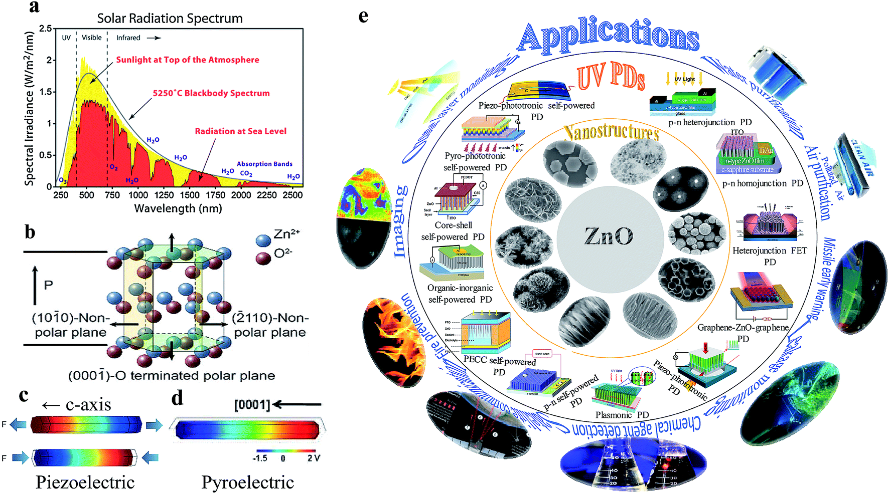 | ||
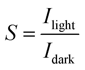
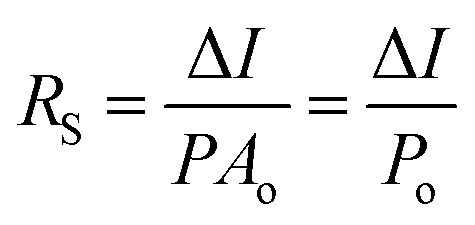
| Fig. 1 (a) Total solar radiation spectrum.12 (b) Atomic model of the ZnO wurtzite structure. Reproduced with permission from ref. 38 Copyright 2012, Wiley-VCH. (c) Simulated piezopotential distribution along a ZnO NW in the presence of strain along the c-axis. Colour gradient indicates the piezopotential generation, where red represents the positive piezopotential and blue the negative piezopotential. Reproduced with permission from ref. 39 Copyright 2009, American Institute of Physics. (d) Electric potential distribution along a ZnO NW when the temperature is decreased from RT 295 to 289 K. Reproduced with permission from ref. 40 Copyright 2012, American Chemical Society. (e) Schematic summarizing the ZnO nanostructures, currently developed UV PDs from conventional to self-powered and their possible future applications. | ||
Over the last decades, UV PDs have been mainly based on thin-film technology, and thus the photosensitivity of PDs is restricted by a limited UV exposure surface area. However, the field of nanotechnology has allowed the direct realization of high-performance UV PDs by introducing high surface-to-volume ratio nanomaterials for multiple photon interactions. Nanomaterials offer tunable and unique optical, electrical, mechanical, and chemical properties over their bulk and thin film counterparts.14–16 Numerous wide bandgap nanomaterials including GaN,17 ZnS,18,19 SiC,20 ZnSe,21 ZnTe,22 In2Te3,23 MoS2,24 Nb2O5,25,26 Ga2O3,27 Zn2GeO4,28 Zn2SnO4,29 TiO2,30 ZnO,31 NiO,32 SnO2,33 and K2Nb8O21![[thin space (1/6-em)]](https://www.rsc.org/images/entities/char_2009.gif) 34 have been explored for UV PD applications. Among them, ZnO is preferable for use in UV PDs because it possesses unique properties, such as a wide direct bandgap (∼3.37 eV), n-type semiconducting behavior, and large exciton binding energy of 60 meV at room temperature, which are attractive features for UV PDs.35,36 Basically, ZnO has three types of crystal structures, including wurtzite, zinc blende, and rock salt, where the thermodynamically most stable phase is wurtzite at ambient pressure and temperature. Wurtzite ZnO has a hexagonal structure belonging to the P63mc space group with the lattice parameters of a = 0.3296 and c = 0.520 65 nm.37 In the ZnO wurtzite structure, the Zn and O atoms are arranged in an hcp pattern and are stacked alternately along the c-axis, where each Zn atom is surrounded by four O atoms and vice versa, forming a tetrahedral non-centrosymmetric structure (Fig. 1b, wurtzite-structured ZnO atomic model).38 Thereby, wurtzite ZnO shows piezoelectric (Fig. 1c) and pyroelectric (Fig. 1d) properties, which are additional features that improve the photoconductivity of ZnO-based UV PDs.39,40 Besides, ZnO is a biocompatible material, which can be applied directly for biomedical applications. Moreover, different dimensional ZnO nanomaterials ranging from 0 to 3D can be obtained for promising nanoscale applications. Fig. 1e shows a schematic summarizing the novel ZnO nanostructures, recently developed ZnO UV PDs and their future applications.
34 have been explored for UV PD applications. Among them, ZnO is preferable for use in UV PDs because it possesses unique properties, such as a wide direct bandgap (∼3.37 eV), n-type semiconducting behavior, and large exciton binding energy of 60 meV at room temperature, which are attractive features for UV PDs.35,36 Basically, ZnO has three types of crystal structures, including wurtzite, zinc blende, and rock salt, where the thermodynamically most stable phase is wurtzite at ambient pressure and temperature. Wurtzite ZnO has a hexagonal structure belonging to the P63mc space group with the lattice parameters of a = 0.3296 and c = 0.520 65 nm.37 In the ZnO wurtzite structure, the Zn and O atoms are arranged in an hcp pattern and are stacked alternately along the c-axis, where each Zn atom is surrounded by four O atoms and vice versa, forming a tetrahedral non-centrosymmetric structure (Fig. 1b, wurtzite-structured ZnO atomic model).38 Thereby, wurtzite ZnO shows piezoelectric (Fig. 1c) and pyroelectric (Fig. 1d) properties, which are additional features that improve the photoconductivity of ZnO-based UV PDs.39,40 Besides, ZnO is a biocompatible material, which can be applied directly for biomedical applications. Moreover, different dimensional ZnO nanomaterials ranging from 0 to 3D can be obtained for promising nanoscale applications. Fig. 1e shows a schematic summarizing the novel ZnO nanostructures, recently developed ZnO UV PDs and their future applications.
This review article focuses on the recent development of UV PDs based on energy-efficient ZnO nanomaterials. The characteristic photodetection parameters, photoconduction mechanism and novel ZnO nanostructures are briefly discussed. The progress and current status of device fabrication approaches ranging from conventional to self-powered are highlighted. Also, recently coupled novel mechanisms such as piezoelectric, pyroelectric and plasmonic effects for performance assistance in ZnO self-powered UV PDs are discussed in detail. Finally, it is summarized by scientifically analyzing the reported literature and concluded with possible future outlooks for next-generation high-performance UV PDs.
2. Characteristic parameters of UV photodetectors
For the detection of a light signal, the bandgap of a photosensitive material should be smaller or equal to the illuminated photon energy. Spectral photoresponse analysis of a UV PD primarily provides information about its UV signal detection limit. For photocurrent generation, the photogenerated electrons and holes need to be separated before recombination upon exposure to UV light on a PD. The response current of a PD is defined as the current generated by a PD under UV illumination, where the current generated only due to UV light can be distinguished. The term sensitivity of a PD provides information related to the signal-to-noise level upon exposure to UV light at a given intensity, and hence, both response current and sensitivity need to be larger for a given high-performance UV PD. The photodetection speed of a PD is another important parameter, which defines how a PD can detect a UV signal or how quickly it goes to its original state after being switched off UV. Primarily, two parameters, response time and recovery time, define the photodetection speed of a PD; hence, a rapid response (smaller values of response time and recovery time) UV PD is extremely important.Furthermore, the additional photoresponse parameter, responsivity, of a PD provides information related to the generation of a response current per unit incident UV illumination power on a PD. In addition to study the noise-related signal of a PD, specific detectivity defines the information associated with the ability to detect a weak UV signal by a PD. In general, the specific detectivity of a PD is related to its noise, which arises from its thermal fluctuations and dark current. Mainly, there are three types of noise present in a PD, including shot noise, Johnson noise and flicker noise, where both Johnson and flicker noise originate from thermal fluctuation, and hence, play an important role in high frequency- and very low frequency-based PD. Table 1 summarizes the typical UV PD parameters and mathematical relations used to evaluate the overall photodetection performance.
| Parameter | Mathematical relation | Unit |
|---|---|---|
| Response current | ΔI = Ilight − Idark; where Idark and Ilight are the currents in absence and presence of UV | Ampere (A) |
| Sensitivity |
|
Unit less |
| Response time | τ r = t90% − t10%; where t10% and t90% are the time at 10% and 90% of the saturation value | Second (s) |
| Recovery time | τ d = t10% − t90% | Second (s) |
| Responsivity |
 ; where P is the UV signal intensity, Ao is the UV signal exposed area and Po is the power of UV signal ; where P is the UV signal intensity, Ao is the UV signal exposed area and Po is the power of UV signal |
Ampere per watt (A W−1) |
| Specific detectivity |
 ; where e is the absolute value of elementary charge ; where e is the absolute value of elementary charge |
Jones |
3. Zinc oxide-based UV photodetectors
For photoconduction in a ZnO UV PD, the photogenerated electrons and holes under exposure to UV illumination are separated by an external (conventional PD) or internal (self-powered PD) driving force. The strength of the driving force plays an important role in the e−–h+ pair separation and recombination process, which determines the overall photoresponse behavior of a PD. The photoresponse mechanism of ZnO-based UV PDs is typically different from that using conventional semiconducting materials, where oxygen molecule adsorption and desorption play a crucial role in photoconduction. In the dark, oxygen molecules adsorb on the ZnO surface from ambient atmosphere according to the equation: O2 (gas) + e− (surface) → O2− (adsorption), and then form a low conductivity depletion region. Under exposure to UV illumination, e−–h+ pairs are photogenerated, where some of the photogenerated holes desorb the adsorbed oxygen molecules from the ZnO surface to decrease the low conductivity depletion width as follows, h+ + O2− (adsorption) → O2 (gas). Finally, the unpaired photogenerated free electrons together with available holes contribute to photoconduction in the presence of an external driving force.41,42Fig. 2 demonstrates the photoconduction mechanism of a ZnO NW-based UV PD (Fig. 2a) with exposure to UV illumination.32 As shown in Fig. 2b (bottom schematic), due to the adsorption of oxygen molecules on the surface of ZnO NW, upward energy band bending takes place due to the formation of a low conductivity depletion layer in the dark (top schematic). Upon exposure to UV illumination, the photogenerated holes migrate to the surface of the NW along the potential slope originating from energy band bending for the desorption of adsorbed oxygen molecules, resulting in a reduction in the low conductivity depletion width. Fig. 2c shows the migration of the photogenerated holes (bottom schematic) for oxygen desorption and decrease in upward energy band bending (top schematic) upon exposure to UV illumination. Again, the oxygen molecules are re-adsorbed when the UV light is turned off and vice versa.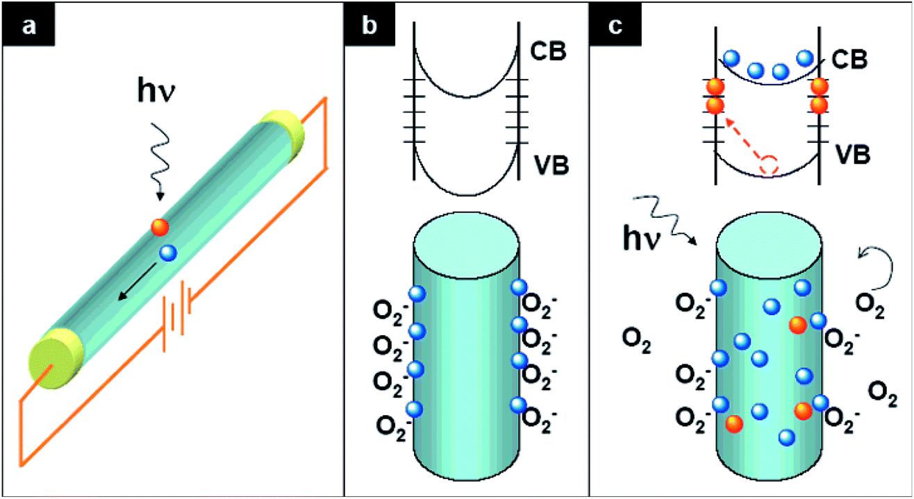 | ||
| Fig. 2 Photoconduction mechanism of ZnO UV PD. (a) Schematic illustration of ZnO NW-based UV PD. (b) Adsorption of oxygen molecules on the surface of ZnO NW in the dark and top schematic depicts the upward energy band banding (valence band (VB) and conduction band (CB)) together with the presence of surface trap states. Bottom schematic shows the capturing of oxygen molecules on the ZnO NW surface. (c) Upon exposure to UV illumination, with photon energy greater or equal to the bandgap of ZnO, electron–hole pairs are photogenerated, where some of the photogenerated holes migrate to the ZnO NW surface for the desorption of adsorbed oxygen molecules (bottom schematic). This effectively decreases the low conductivity depletion width of NW. The unpaired electrons together with the free photogenerated holes contribute to the photocurrent under an external driving force. Reproduced with permission from ref. 42 Copyright 2007 American Chemical Society. | ||
Various ZnO nanomaterials including NWs,43 nanorods (NRs),44 nanotubes (NTs),45 nanobelts (NBs),46 nanoflakes (NFs),47 nanoparticles (NPs),48 and quantum dots (QDs)49 have been utilized to improve the performance of UV PDs. Nanomaterials basically show efficient photoconduction behavior compared to their bulk and thin film counterparts due to their large surface-to-volume ratios. Hence, many physical and chemical synthetic approaches have been used for the synthesis of ZnO nanostructures, such as pulsed laser ablation,50 molecular beam epitaxy,51 vapor phase transport,52 electrochemical deposition,53 metal organic chemical vapor deposition,54 physical vapor deposition,55 chemical vapor deposition,56 wet-chemical-based methods such as sol–gel57 and hydrothermal/solvothermal growth.58,59 Among them, recently, the wet-chemical-based approach has been widely applied due to its advantages such as relatively low temperature synthesis (mostly below 150 °C), cost-effective and simple synthetic processes, and controllable nanostructure morphology, surface and dimensions.60–65 Additionally, it allows the direct growth of nanostructures on conductive or flexible plastic substrates.66,67 As shown in Fig. 3, different dimensional ZnO nanostructures such as 3D (microflowers,68 hierarchical superstructures,69 superstructures,70 hierarchical structures,71etc.), 2D (nanosheets,72 nanoflakes,73 nanodisks,74 mesoporous single-crystal sheets,75etc.), 1D (NWs,76 NRs,77 NTs,78 NBs,79etc.) and 0D (QDs,80 NPs,81 core–shell structures,82 hollow spheres,83etc.) structures can be synthesized vie the wet-chemical process.
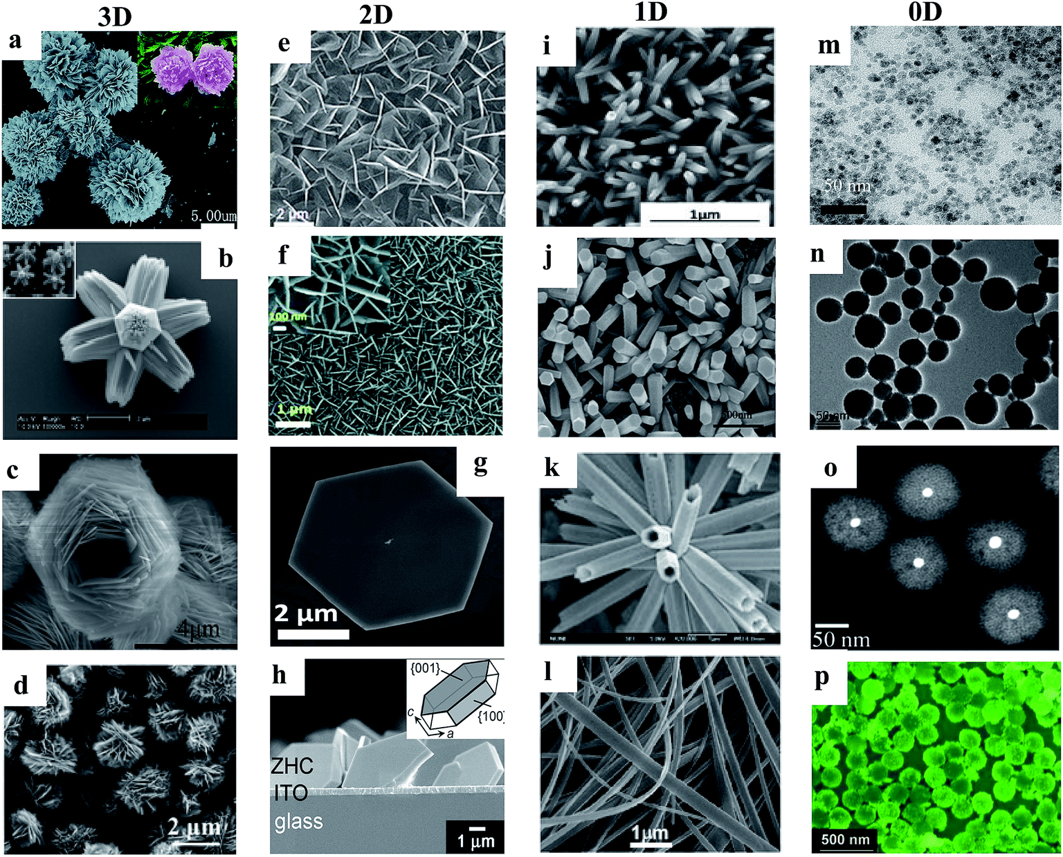 | ||
| Fig. 3 Various dimensional ZnO nanostructures synthesized via the hydrothermal process. 3D: (a–d) microflowers,68 hierarchical superstructures,69 superstructures70 and hierarchical structures.71 2D: (e–h) nanosheets,72 NFs,73 nanodisks74 and mesoporous single-crystal sheets.75 1D: (i–l) NWs,76 NRs,77 NTs78 and NBs79 and 0D: (m–p) QDs,80 NPs,81 core–shell structures82 and hollow spheres.83 Reproduced with permission from ref. 68–83 Copyright 2015 Royal Society of Chemistry. Copyright 2006 American Chemical Society. Copyright 2012 American Chemical Society. Copyright 2013 American Chemical Society. Copyright 2013 American Chemical Society. Copyright 2016 Royal Society of Chemistry. Copyright 2014 Royal Society of Chemistry. Copyright 2017 American Chemical Society. Copyright 2013 IOP. Copyright 2013 WILEY-VCH. Copyright 2013 Royal Society of Chemistry. Copyright 2006 Royal Society of Chemistry. Copyright 2015 Royal Society of Chemistry. Copyright 2010 WILEY-VCH. Copyright 2015 American Chemical Society. Copyright 2011 WILEY-VCH. | ||
3.1 Conventional UV photodetectors
Conventional ZnO UV PDs are mostly operated by an external driving force in terms of voltage or current source. Upon exposure to UV illumination, photogenerated electrons and hole are driven by the externally applied driving force for the generation of a photocurrent. Therefore, the external driving force plays an important role in photogenerated electron and hole recombination, separation and transportation processes, which determine the overall photoresponse behavior of a conventional PD. Based on the device design and working mechanisms, conventional ZnO UV PDs can be classified into different categories.Recently, atomically-thin 2D graphene was used with ZnO for the efficient collection of photogenerated charges in UV PDs due to its inherent intrinsic properties, such as outstanding mobility, transparency, mechanical stability, and flexibility. A generated built-in electric field at the interface of graphene and ZnO offers efficient charge separation and transportation for rapid photoconduction under an external driving force.111–113 We fabricated a ZnO NW/graphene foam heterostructure for UV PD application, where highly dense ZnO NWs were direct grown on 3D graphene foam for efficient charge conduction and separation.114 As shown in Fig. 4a, first graphene foam was grown on 3D nickel foam followed by CVD, and then the nickel template was etched to directly grow ZnO NWs on graphene foam via the thermal evaporation technique. Fig. 4b shows a schematic diagram of the PD, and its respective I–V responses in both the absence and presence of UV are shown in Fig. 4c. Under UV illumination (365 nm, 1.3 mW cm−2), the current of the PD increased due to the increase in conductivity, where the cyclic photoresponse of the PD is depicted in Fig. 4d. At a bias voltage of 5 V, the PD showed a current response of 700 μA and response time/recovery time of 9.5 s/38 s (Fig. 4e). With an increase in the bias voltage of the PD, the response current increased due to the increase in the drift velocity of charge carriers, where an ∼868% enhancement in response current was observed at a bias voltage of 8 V compared to that at a bias voltage of 1 V (Fig. 4f). Moreover, we reported a ZnO NW/graphene heterostructure UV PD (Fig. 4g),84 graphene/ZnO NW/graphene UV PD (Fig. 4h),115 and graphene-ZnO QDs-graphene UV PD (Fig. 4i),80 where faster and higher photoresponses were measured under UV illumination, and their overall photoresponse performances are listed in Table 2.
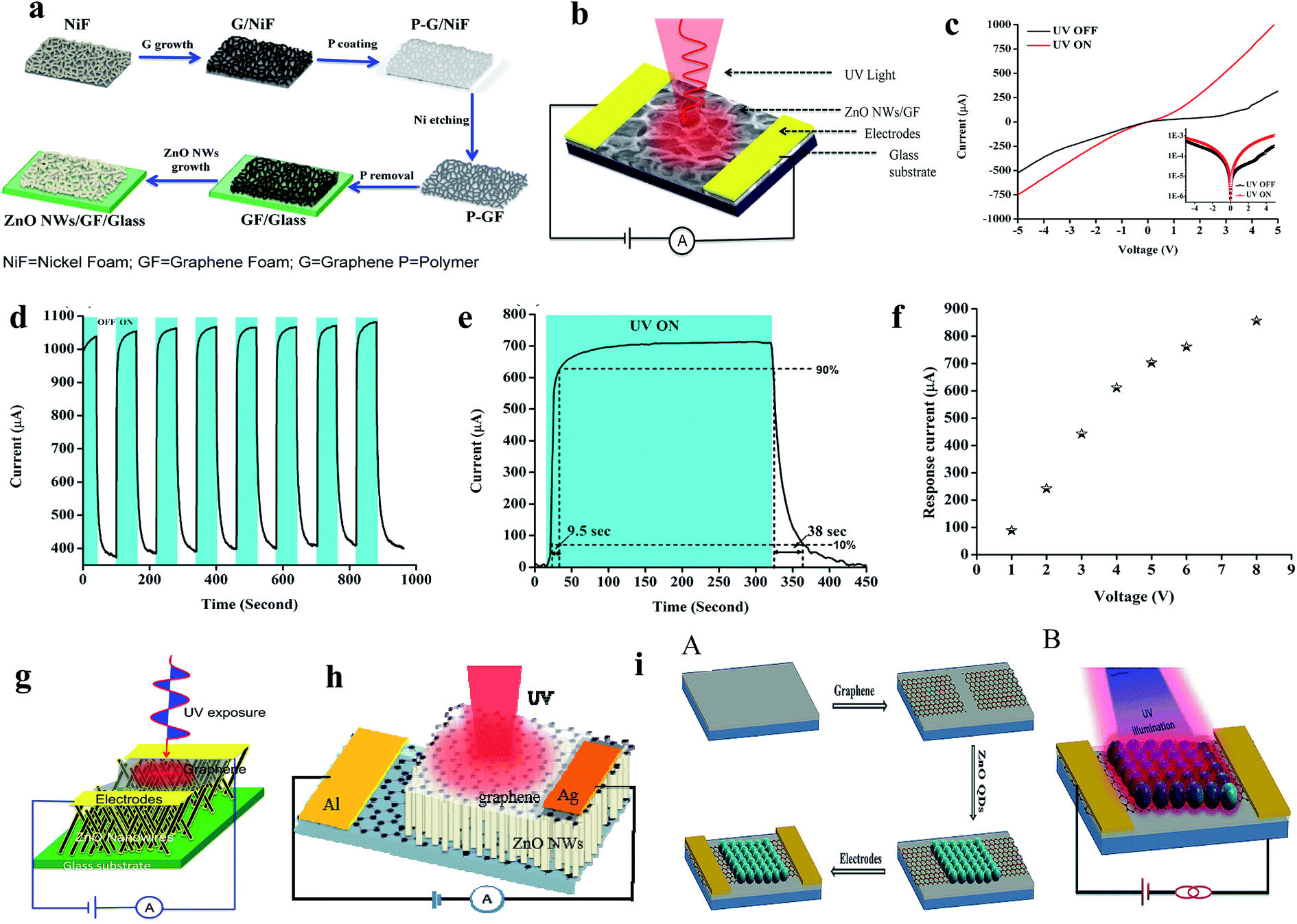 | ||
| Fig. 4 (a and b) Schematic representation of the steps involved in the fabrication of a UV PD and schematic diagram the as-fabricated PD, respectively. (c and d) I–V responses in both the absence and presence of UV (365 nm, 1.3 mW cm−2) and cyclic photoresponse of the PD at a bias voltage of 5 V, respectively. (e) Estimation of response time and recovery time of the PD. (f) Response current as a function of bias voltage plot. Reproduced with permission from ref. 114 Copyright 2015 American Chemical Society. (g) ZnO NWs/graphene heterostructure PD. Reproduced with permission from ref. 84 Copyright 2015 IOP. (h) Graphene/ZnO NWs/graphene PD. Reproduced with permission from ref. 115 Copyright 2016 IOP. (i) Graphene-ZnO QDs-graphene PD: (A and B) schematic diagram of the fabrication processes in the PD and schematic diagram of the PD, respectively. Reproduced with permission from ref. 80 Copyright 2015 Royal Society of Chemistry. | ||
| PD | Bias | UV light | Response current | Response time & recovery time | Sensitivity | Responsivity | Specific detectivity |
|---|---|---|---|---|---|---|---|
| ZnO NWs165 | 1 V | 360 nm | 34 nA | 2 s &100 s | 12.26 | 0.39 A W−1 | 1.9 × 10⁸ Jones |
| ZnO NWs166 | 3 V | 352 nm | — | 5 s & 100 s | — | — | — |
| ZnO NWs146 | 3 V | 310 nm | 5.13 μA | 229 s & 547 s | — | — | — |
| ZnO NRs167 | 325 nm | — | 3.7 s& 63.6 s | — | — | — | |
| ZnO NW/graphene foam114 | 5 V | 365 nm | ∼700 μA | 9.5 s & 38 s | 6 A W−1 | ||
| ZnO NR/graphene148 | 20 V | 370 nm | 22.7 A W−1 | ||||
| ZnS/ZnO bilayer film145 | 5 V | 350 nm | ∼180 μA | 50 s & 50 s | ∼1066 | 94 A W−1 | |
| ZnO-SnO2 nanofiber film151 | 10 V | 300 nm | ∼7.9 nA | 32.2 s & 7.8 s | ∼5000 | ||
| ZnO NP-graphene core–shell149 | 20 V | 375 nm | 9 ms & 11 ms | 600 | 640 A W−1 | ||
| Graphene/ZnO NWs84 | 5 V | 365 nm | 3.02 mA | 11.9 s & 240 s | 32000 A W−1 |
3.9 × 10¹³ Jones | |
| Graphene/ZnO NW/graphene115 | −5 V | 365 nm | ∼300 μA | 3 s & 0.47 s | 23 A W−1 | ||
| Co-ZnO NRs168 | 5 V | 365 nm | 80 μA | 1.2 s & 7.4 s | 760 A W−1 | ||
| Monolayer graphene/ZnO NRs124 | −1 V | 365 nm | 0.7 ms & 3.6 ms | 113 A W−1 | |||
| Graphene/ZnO NW/graphene169 | 3 V | 325 nm | 0.7 s & 0.5 s | 8 × 10² | 0.42 A W−1 | ||
| Graphene-ZnO QDs-graphene80 | 2 V | 365 nm | ∼720 nA | 0.29 s & 0.29 s | ∼109 Jones | ||
| ZnO granular NWs43 | 1 V | 365 nm | ∼1 μA | 0.56 s & 0.32 s | 7.5 × 10⁶ A W−1 | 3.3 × 10¹⁷ Jones | |
| ZnO NR network170 | 4 V | 365 nm | 2 s & — | 1.8 | |||
| ZnO NW array171 | 5 V | 370 nm | 0.1 ms & 0.4 ms | 1.4 | |||
| ZnO spatial tetrapod network172 | 1 V | 365 nm | 0.4 s & 0.3 s | 106 | |||
| ZnO nanotetrapod network173 | 2.4 V | 365 nm | 67 ms & 30 ms | 4.5 × 10³ | |||
| NiO/ZnO141 | −5 V | 310 nm | 100 | 21.8 A W−1 | 1.6 × 10¹² Jones | ||
| ZnO/Si138 | −2 V | 365 nm | — | — | — | 0.34 A W−1 | 2.11 × 10¹⁰ Jones |
| ZnS-coated ZnO array146 | 3 V | 310 nm | 162 μA | 229 s & 547 s | — | ||
| ZnS/ZnO biaxial nanobelt144 | 5 V | 320 nm | 3.97 μA | 0.3 s & 1.7 s | 6.9 | ||
| ZnS-ZnO bilayer film145 | 5 V | 370 nm | ∼16 μA | 50 s & 50 s | 1066 | ||
| ZnO-SnO2 nanofibers film151 | 10 V | 300 nm | ∼7.9 nA | 32.2 s & 7.8 s | 4600 | — | — |
| Electrospun ZnO NWs/PbS QDs174 | 10 V | 350 nm | — | — | — | 51 mA W−1 | 3.4 × 10⁸ |
| Ag@ZnO NWs120 | 5 V | 365 nm | ∼25000 μA |
1.02 s & 15.5 s | ∼11.2 | — | — |
| ZnO film with Ag NPs121 | 5 V | 380 nm | — | ∼15 s & ∼330 s | — | 2.86 A W−1 | — |
| p-CuSCN/n-ZnO NRs175 | −3 V | 365 nm | — | 3.2 s & 3.8 s | — | 22.5 mA W−1 | — |
| Al NPs-ZnO NRs122 | 5 V | 325 nm | ∼18 μA | 0.8 s & 0.85 s | — | 1.59 A W−1 | — |
| ZnO-PEDOT:PSS176 | 5 V | 252 nm | 674 μA | — & 15 s | 37.65 | 5.046 A W−1 | — |
| ZnO QD/graphene nanocomposite177 | 365 nm | 2 s & 1 s | 1.1 × 10⁴ | — | — | ||
| SnO2-coated ZnO NWs178 | 0.8 V | 325 nm | 109 nA | 1.5 s & 25.6 s | 4.516 | — | — |
| ZnO NPs film83 | 5 V | 350 nm | 2.55 μA | 0.467 ms & 0.94 ms | 52 | — | — |
| C-doped ZnO/rGO179 | 1 V | 334 nm | 0.1 nA | 120 ms & 80 ms | 1.3 | — | — |
| Sn-doped ZnO NRs180 | 5 V | UV lamp | 17.7 μA | — | 60 | — | — |
| La-doped ZnO NWs181 | 10 V | 365 nm | 481 nA | — | 2.6 | — | — |
| Al-doped ZnO NWs182 | 1 V | 365 nm | 62 μA | 0.1 s & 20 s | 6.2 × 10⁵ | 3.8 A W−1 | — |
| Cu-doped ZnO NRs183 | — | UV lamp | 23 μA | 2.7 s & 118 s | 5.6 × 10⁴ | — | — |
| Ga-doped ZnO nanopagodas184 | 1 V | 254 nm | 28.3 μA | 0.53 s & 14 s | 1.3 | — | — |
| Mg-doped ZnO NRs185 | 1 V | 365 nm | 8 μA | 24.5 s & 18.4 s | 5.2 | — | — |
| In-doped ZnO NRs186 | 1 V | UV lamp | 49.3 μA | — | 71.4 | 2.5 A W−1 | 1.44 × 10¹¹ Jones |
Moreover, ZnO nanostructures were directly grown on carbon nanotubes (CNTs) for direct charge conduction, where CNTs provide rapid charge carrier transportation, for instance, Hart's group fabricated ZnO NWs-coated aligned CNTs,116 where a faster photodetection performance of 0.25 s response time and 0.35 s recovery time was measured due to the direct transportation of photogenerated charges through aligned CNTs, which effectively reduced the recombination rate of the photogenerated electrons and holes under UV illumination. In addition, we fabricated ZnO QD-decorated CNTs for UV PD application,117 and nearly 275% enhancement in response current was measured at 1 V bias voltage compared to the pristine ZnO QD PD.
The localized surface plasmon resonance (LSPR) effect of nanomaterials results in unique light absorption capacity, which photoexcites electrons in contact with ZnO upon exposure to UV light, thereby modifying the photoconduction. Fundamentally, nanomaterials (preferably NPs) based on noble metals such as Au,118,119 Ag,120,121 Al,122 and Pt,123 have attracted special attraction due to their efficient LSPR effects and widely coupled with ZnO nanomaterials for photoconduction enhancement. Liu et al. reported Ag NPs-decorated ZnO NWs for application in UV PDs, as shown in Fig. 5a (device schematic).120 It can be seen from the I–V characteristics (Fig. 5b) that upon exposure to UV light, the Ag NP-decorated ZnO NWs showed a higher photoresponse compared to their bare counterpart due to the enhancement in light absorption, which is related to the LSPR effect of Ag NPs. Fig. 5c shows the energy band of the Ag and ZnO heterojunction (top schematic), where under exposure to UV light, electrons and holes are photogenerated and hot electrons transferred from the Ag NPs to the CB of ZnO (bottom schematic), thereby enhancing the photoconduction. Similar results were also reported by Wang and co-authors, where Ag NPs were decorated on top of a ZnO film for application in a UV PD, as shown in Fig. 5d (device schematic).121 As shown in Fig. 5e, the Ag NP-decorated ZnO PD displayed a higher photoresponse performance compared to the pristine ZnO PD due to the LSPR effect of the Ag NPs. Lu and co-authors demonstrated an Al NP-decorated ZnO NR UV PD, where a superior enhancement in responsivity from 0.12 to 1.59 A W−1 and nearly 6-fold enhancement in sensitivity were measured in the Al NP-decorated ZnO NR PD compared to the pristine ZnO NR PD due to the localized surface plasmons (LSPs) of the Al NPs.122 The authors also reported that the Al NP-decorated ZnO NR PD showed a faster photodetection speed of 0.030 s (response time) and 0.035 s (recovery time) compared to that of the bare PD of 0.80 s and 0.85 s, respectively, mainly due to the rapid resonant couplings between the LSPs of the Al NPs and excitons of the ZnO NRs. An Au NP-decorated ZnO NW UV PD was fabricated by Liu et al.,119 where ∼103 times enhancement in the sensitivity in Au NP-decorated ZnO NW PD was reported compared to that in the pristine ZnO NW PD due to the plasmonic enhancement in the light absorption efficiency of the Au NPs. In addition, an improvement in recovery time from ∼300 to ∼10 s was reported in the Au NP PD.
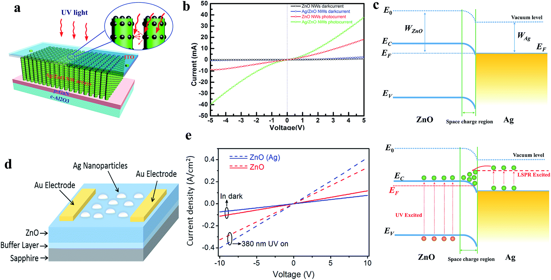 | ||
| Fig. 5 (a and b) Schematic representation of Ag NPs/ZnO NW-based plasmonic PD and the respective I–V profiles with and without UV illumination (365 nm, 0.24 mW cm−2), respectively. (c) Energy band diagrams of the Ag/ZnO heterojunction (top schematic) and LPSR excited electrons transfer from Ag to ZnO upon exposure to UV illumination (bottom schematic). Reproduced with permission from ref. 120 Copyright 2014 Optical Society of America. (d) Schematic diagram of Ag NPs decorated ZnO-based PD. (e) J–V characteristics of pristine ZnO and Ag NPs decorated ZnO based PDs in both the presence and absence of UV light. Reproduced with permission from ref. 121 Copyright 2017 American Chemical Society. | ||
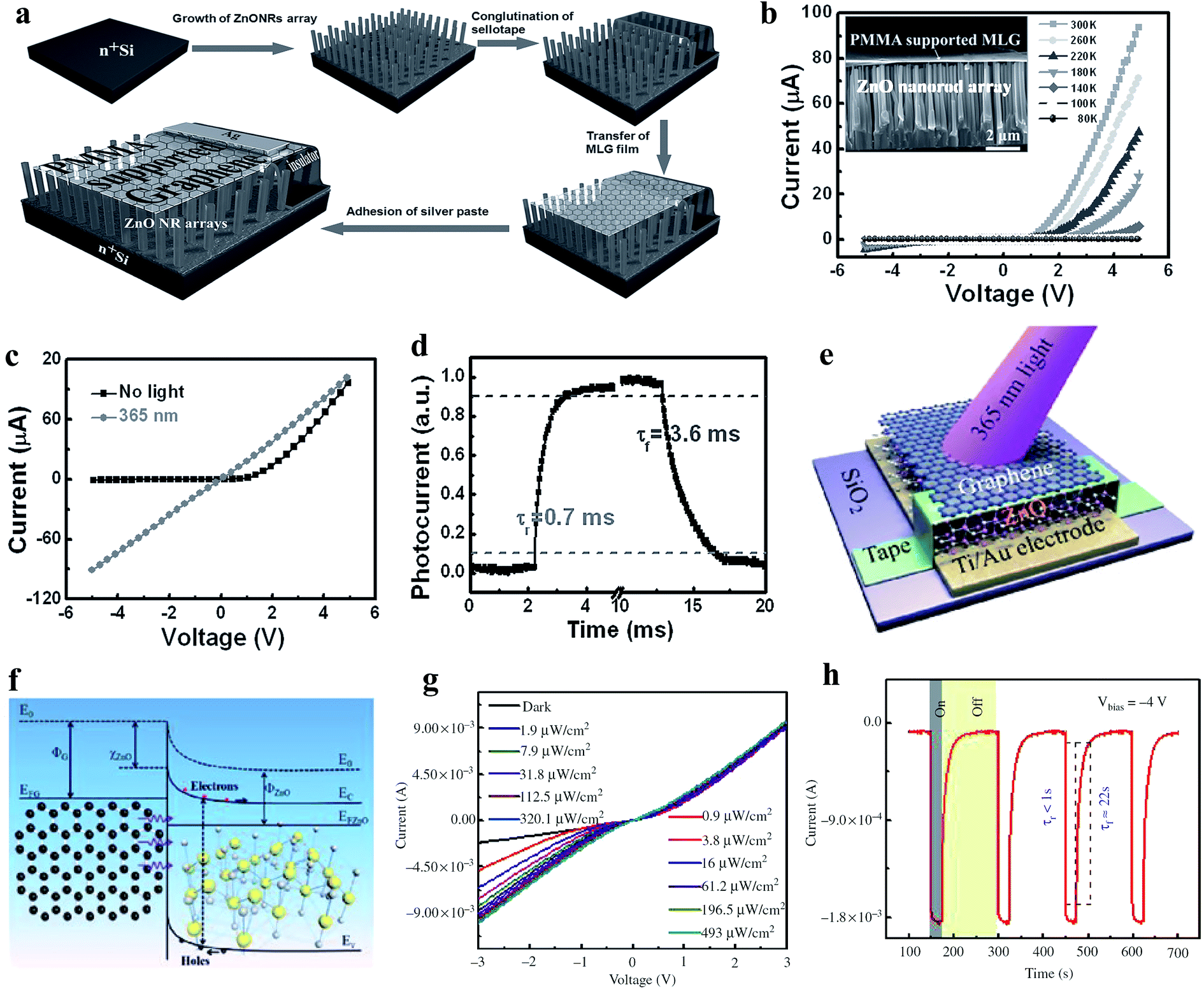 | ||
| Fig. 6 (a) Schematic illustration of the processes involved in the fabrication of MLG film/ZnO NR PD. (b) I–V characteristics at different operational temperatures (80 to 300 K) of the PD, inset depicts the typical cross-sectional SEM image of the PMMA-supported MLG film/ZnO NR junction. (c and d) I–V responses recorded with and without 365 nm UV illumination and estimation of response time/recovery time of the PD, respectively. Reproduced with permission from ref. 124 Copyright 2013 Wiley-VCH. (e and f) Schematic diagram of the graphene-ZnO Schottky junction-based PD and the respective energy band diagram of the PD under exposure to UV light illumination, respectively. (g and h) I–V responses at different UV illumination (365 nm) intensities and estimation of response time/recovery time of the PD, respectively. Reproduced with permission from ref. 125 Copyright 2016 De Gruyter. | ||
Likewise, Zhang et al. reported a graphene-ZnO Schottky junction-based PD, as shown in Fig. 6e, for high-performance photoconduction, where Fig. 6f depicts a schematic illustration of the respective energy band diagram of the graphene-ZnO Schottky junction under exposure to UV illumination.125 Under a reverse bias condition, the strength of the Schottky barrier height was enhanced to reduce the dark current. Upon exposure to UV light, the photogenerated electrons were transported from ZnO to graphene by crossing the barrier to generate a photocurrent. Fig. 6g shows the I–V characteristics both in the absence and presence of UV illumination at different intensities, where with an increase in UV illumination intensity, the current in the reverse bias direction increased due to the increase in the electron and hole generation efficiency. The asymmetric I–V profiles demonstrated Schottky junction formation between graphene and ZnO. The fabricated PD displayed a response time and recovery time of <1 s and 22 s (Fig. 6h), respectively. The authors noted that because of the existence of defect states such as O and Zn vacancies or excess Zn and O atoms in ZnO, the PD exhibited a relatively slow response under exposure to UV light. Moreover, the authors reported a high responsivity of 3 × 10⁴ A W−1 and specific detectivity of 4.33 × 10¹⁴ Jones in the reverse bias condition.
 | ||
| Fig. 7 Al, N-codoped p-type ZnO film and n-type ZnO NW-based homojunction: (a and b) schematic diagram and cross-sectional SEM image (scale bar is 500 nm) of the p–n homojunction PD, respectively. (c and d) I–V characteristics recorded with and without UV light and spectral photoresponses of the PD, respectively. Reproduced with permission from ref. 126 Copyright 2010 American Institute of Physics. Sb-doped p-type ZnO NWs and n-type ZnO film based homojunction: (e and f) schematic diagram of the homojunction PD and the respective I–V characteristics before and after exposure to UV, respectively. (g) Photocurrent spectra of the PD at different reversed bias voltages. Reproduced with permission from ref. 127 Copyright 2011 American Institute of Physics. | ||
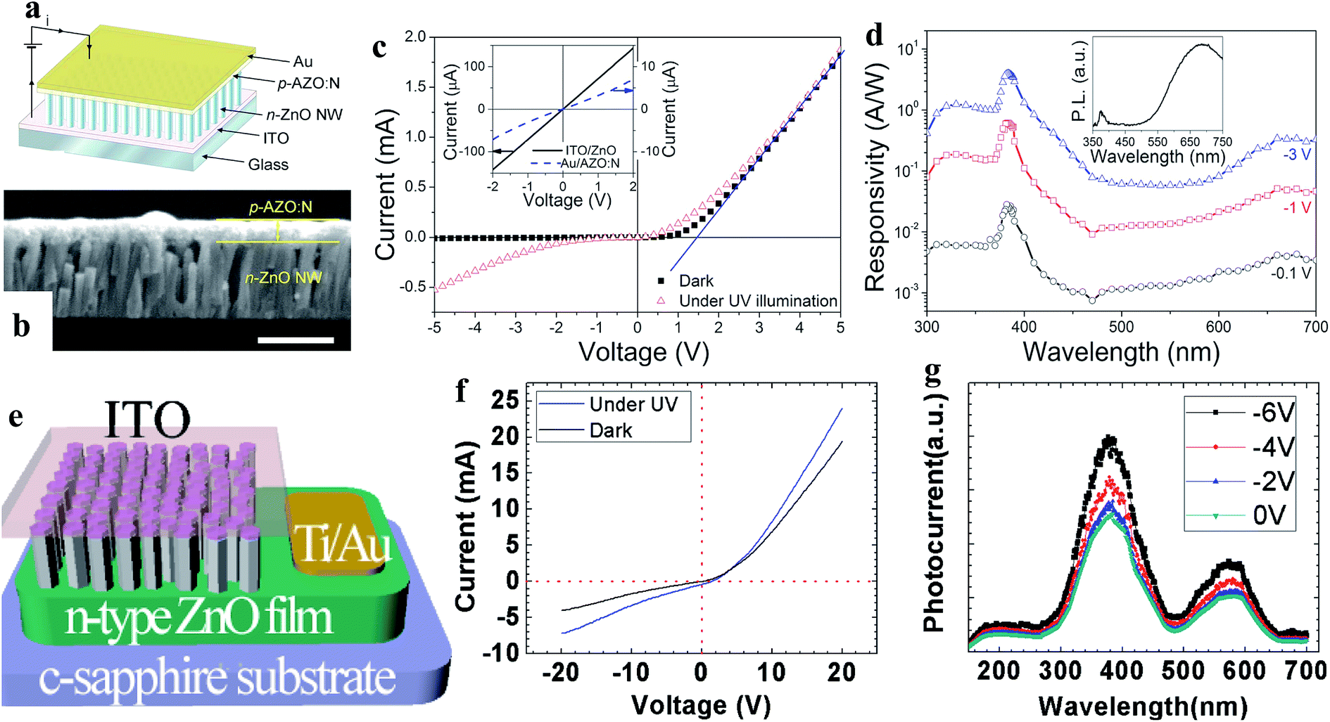
Heterojunctions of ZnO nanomaterials with other semiconductors have been introduced to form p–n junctions or n–n junctions depending on the photoactive materials for UV PDs, for example, ZnO/Si heterojunction,138 ZnO NWs/p-GaN heterojunction,139 n-Ga:ZnO NRs/p-GaN heterojunction,140 NiO/ZnO heterojunction,141 ZnO/GaN heterojunction,142 ZnS-ZnO heterojunction,143–146 p-GaN/n-ZnO NRs heterojunction,147 ZnO NR/graphene heterostructure,148 and ZnO NP-graphene core–shell heterostructure.149 Unlike homojunctions, photogenerated electrons and holes are separated by internally generated and externally applied electric fields under UV illumination. Hence, the selection of the semiconductor material to form heterojunctions with ZnO is important, which defines the strength of the internal electric field. As shown in Fig. 8a (device schematic), Tsai and co-authors reported p-type NiO with n-type ZnO for a p-NiO/n-ZnO heterojunction UV PD.150 The energy band diagram of the respective p-NiO/n-ZnO heterojunction is illustrated in Fig. 8b, confirming the generation of a built-in electric field due to the Fermi level alignment. Diode-like characteristics (Fig. 8c, I–V) with a leakage current of 6.64 × 10⁻⁸ A cm−2 were obtained in the PD. Upon UV illumination on the PD, the current increased in both the forward and reversed bias directions and the current sensitivity of 11.56 was measured at a reverse bias voltage of −1 V. No additional photodetection parameters for the heterojunction PD were reported by the authors. Tian and co-authors fabricated a ZnO and SnO2 (n–n) heterojunction (ZnO/SnO2) UV PD, as illustrated Fig. 8d (energy band diagram).151 It can be seen from the schematic (Fig. 8d) that the photogenerated holes move from SnO2 to ZnO and electrons from ZnO to SnO2 due to the internal built-in electric field, which facilitates the overall photoconduction process upon exposure to UV illumination. As shown in Fig. 8e, the typical I–V profiles recorded with and without light illumination (250 to 400 nm) showed photoconduction behavior. Under UV light illumination of 300 nm (0.45 mW cm−2 intensity) on the PD, the current increased from 1.7 pA to 7.9 nA (∼4600 times enhancement) at a bias voltage of 10 V. Likewise, effective increments in the current were reported when the PD was exposed to light sources of 250 nm, 280 nm, 320 nm and 350 nm. The highest sensitivity of ∼5 × 10³ was measured upon exposure to 300 nm wavelength on the PD due to the highest light power intensity. Moreover, the PD showed a sensitive response upon exposure to 400 nm light having energy below than the band gaps of ZnO and SnO2, which was mainly due to the possible transition of carriers from the defect states to the CB. As shown in Fig. 8f, the spectroscopic photoresponse and inset (absorption spectrum) of the PD confirmed its UV sensitive photoresponse with an exhibited threshold excitation energy of 3.6 eV, which is close to the bandgap energy of the ZnO/SnO2 heterojunction. The measured photodetection speed for the ZnO/SnO2 heterojunction PD was 32.2 s (response time) and 7.8 s (recovery time). Likewise, Fang's group fabricated a ZnS/ZnO biaxial NB based high-performance UV PD,152 where efficient photodetection performances were measured in the ZnS/ZnO heterostructure compared to the pure ZnS or ZnO nanostructures due to the internal built-in electric field. The authors reported the a wide-range UV-A light photoresponse in the wavelength range from around 200 to 380 nm, ultra-high responsivity of 5.0 × 10⁵ A W−1 at a bias voltage of 5 V, and response time of <0.3 s and recovery time of 1.5 s. Therefore, it can be concluded that junction-based UV PDs show a higher photodetection performance compared to their pristine counterparts due to synergistic effects and generated internal electric fields.
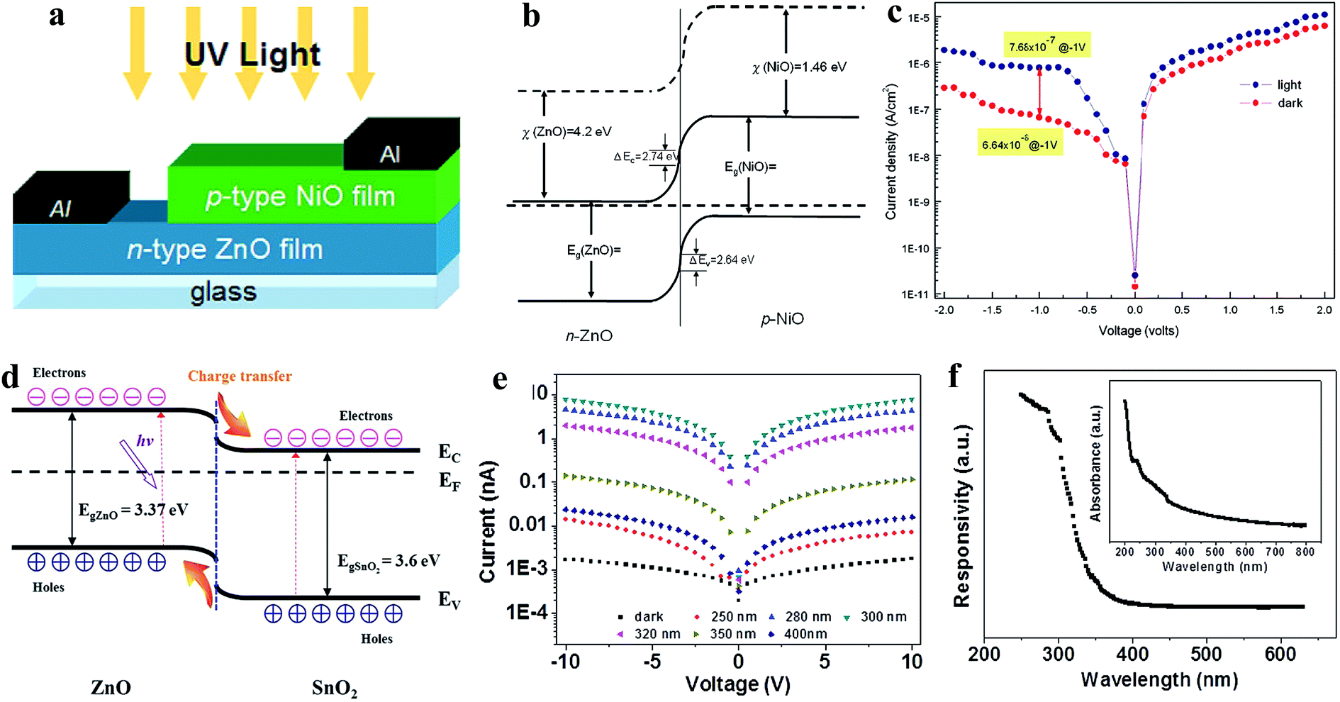 | ||
| Fig. 8 Transparent p-NiO/n-ZnO heterojunction PD: (a and b) schematic illustration of p-NiO/n-ZnO heterojunction PD and the respective energy band diagram, respectively. (c) J–V characteristics of the p-NiO/n-ZnO heterojunction PD recorded before and after exposure to UV illumination. Reproduced with permission from ref. 150 Copyright 2011 Elsevier. ZnO-SnO2 heterojunction PD: (d and e) energy band diagram and I–V profiles of the ZnO-SnO2 heterojunction PD in both the absence and presence of light illumination of different wavelengths (250 to 400 nm), respectively. (f) Spectroscopic photoresponse profile at a bias voltage of 5 V and inset depicts the absorption spectrum. Reproduced with permission from ref. 151 Copyright 2013 WILEY-VCH. | ||
As mentioned earlier, ZnO displays a piezoelectric effect due to its noncentral-symmetric crystal structure, where 1D ZnO nanomaterials show a higher piezoelectric response due to their c-axis orientation. Under external force/strain, piezoelectric potentials are generated across 1D nanomaterials, which can be considered to control photogenerated charge carrier separation, transportation, generation and recombination.153–155 Therefore, currently, the piezoelectric effect is considered an additional advantage of ZnO, which helps in tuning the photoconductivity of PDs. Wang's group developed a ZnO/ZnS heterojunction core/shell NW PD, where the piezo-phototronic effect was introduced for photoresponse enhancement.156 As illustrated in Fig. 9a, ZnO/ZnS core/shell NWs were directly grown on an ITO-coated glass substrate, then an Ag/polyester zigzag electrode was connected on top of the NWs and external compressive loads were applied from the Ag/polyester zigzag electrode, where UV illuminated the ITO substrate. The as-fabricated PD displayed a highly sensitive response to UV (385 nm), blue and green illumination, as depicted in Fig. 9b (I–V responses). It was concluded that under light illumination, with photon energy smaller than the band gaps of ZnO and ZnS, indirect type-II transitions of electrons from the VB (ZnO) to CB (ZnS) take place at the interface of the ZnO core and ZnS shell. Moreover, the authors enhanced the photoconduction performance of the PD by coupling the piezo-phototronic effect, which facilitated the lowering of the barrier height across the ZnO/ZnS interface for easy charge carrier transportation, and hence an increase in current with an increase in external load (Fig. 9c, I–V curves at different loads ranging from 0.05 to 0.4 kg force (kgf) under UV illumination of 1.32 mW cm−2 intensity). A large enhancement of ∼31 times in the peak photocurrent at 0.4 kgf was reported compared to that in the absence of a load under exposure to UV illumination. Similar responses of ∼18 times for blue (465 nm, 3 mW cm−2) and ∼19 times for green (520 nm, 3.2 mW cm−2) excitation were reported in the presence of an external load. The calculated responsivities at 0.4 kgf compressive load under exposure to 385 nm (1.32 mW cm−2), 465 nm (3 mW cm−2) and 520 nm (3.2 mW cm−2) illumination were 2.5 A W−1, 0.54 A W−1 and 0.13 A W−1, respectively at a bias voltage of 1.5 V, which are nearly an order of magnitude higher than that with no load. Fig. 9d shows the comparative change in the responsivity ((RLoad − Ro/Ro) × 100%, where RLoad and Ro are the responsivities with and without load, respectively) plots with respect to the applied compressive load, which increased with an increase in the external load due to the increase in the piezo-phototronic effect. The associated piezo-phototronic effect can be explained from the schematic diagrams in Fig. 9e, where (i) and (ii) are the band diagrams of the PD before and after bend alignment, respectively. The direct band to band and indirect type-II transitions of electrons under exposure to light in the absence of an external load are depicted in Fig. 9e(iii). As shown in Fig. 9e(iv), the generation of piezopotentials across the ZnO NRs led to band bending for efficient charge carrier transportation across the ZnO/ZnO interface under illumination in the presence of external compressive strain.
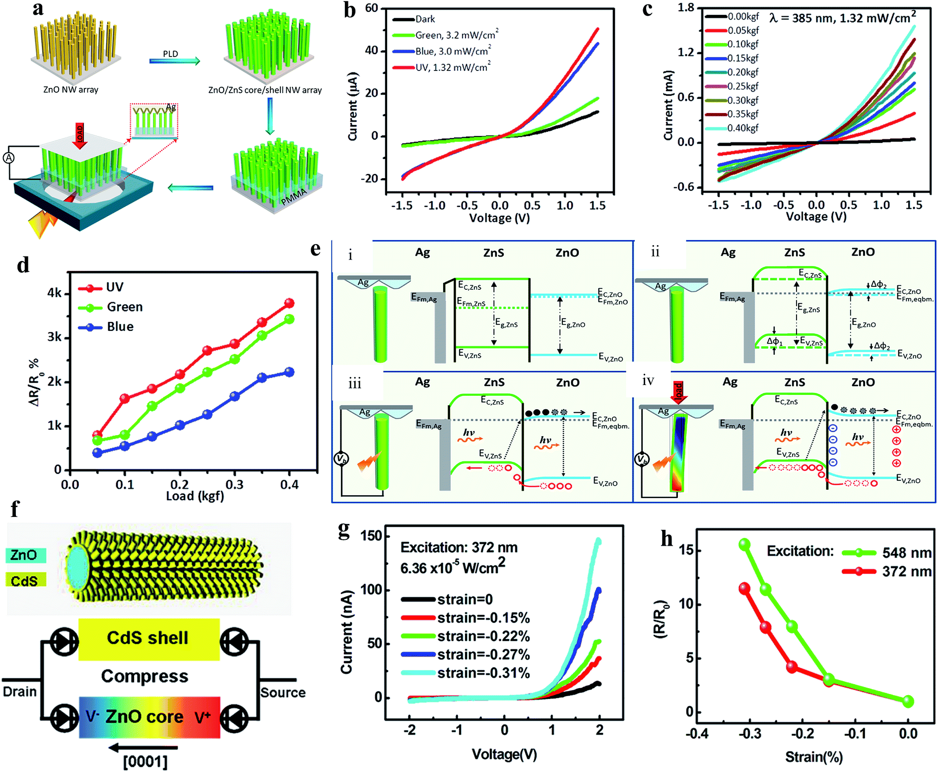 | ||
| Fig. 9 ZnO/ZnS heterojunction core/shell NWs PD: (a) schematic illustration of the processes involved in fabrication of the ZnO/ZnS core/shell NWs PD. (b) I–V responses measured before and after exposure to green, blue and UV light. (c) I–V profiles at a fixed exposure to UV light of intensity of 1.32 mW cm−2 at different compressive loads. (d) Change in responsivity with respect to compressive load under light illumination. (e) Photoconduction mechanism of the PD under compressive load: (i) and (ii) are the energy band diagrams of the Ag/ZnS/ZnO interface before and after the alignment of the Fermi levels, respectively. (iii) and (iv) are the schematics of the direct band-to-band and indirect type-II transitions of electrons from the VB to CB under light illumination in the absence and presence of compressive strain, respectively. In the presence of compressive strain together with light illumination, piezopotential-induced band bending occurs across the ZnO/ZnS interface. Reproduced with permission from ref. 156 Copyright 2015 American Chemical Society. ZnO/CdS core–shell micro/NWs: (f) 3D structure representation of a ZnO/CdS core–shell wire (top schematic) and the respective proposed sandwich model of the PD composed of two back-to-back Schottky diodes integrated into a ZnO core and CdS shell structure under compressive strain (bottom schematic). (g) I–V responses of the PD at different compressive strains in the presence of UV. (h) Change in responsivity with respect to compressive strain under exposure to green light (548 nm) and UV light (372 nm), where R and R0 are the responsivities with and without compressive strain, respectively. Reproduced with permission from ref. 157 Copyright 2012 American Chemical Society. | ||
Zhang and co-authors fabricated piezo-phototronically modulated a ZnO/CdS core–shell micro/NW-based PD, as illustrated in Fig. 9f (top schematic), and the bottom schematic shows the proposed model of the PD integrated with back-to-back Schottky diodes under compressive strain.157 Remarkably, the photoconduction of the PD increased with an increase in compressive strain under steady state UV illumination (372 nm, 6.36 × 10⁻⁵ W cm−2) (Fig. 9g). It was found that the photocurrent of the PD increased from 12.9 to 144 nA when the strain increased to −0.31% at a positive bias voltage of 2.0 V. A similar response was also noticed when the PD was illuminated by green light (548 nm, 1.43 × 10⁻³ W cm−2). As depicted in Fig. 9h, with the change in responsivity with compressive strain under both green and UV light illumination, nearly more than 10 times enhancement in the responsivity of the PD was measured under −0.31% strain compared to that in the unstrained condition. Moreover, Luo and coauthors fabricated a p-NiO/n-ZnO type piezo-phototronic-based UV PD, and the recovery time of the PD was notably improved through modulation of its piezopotentials.158 An Au-MgO-ZnO NW piezo-phototronic-based UV PD was reported by Zhang's group.159 They effectively enhanced the sensitivity of the PD by controlling the piezo-phototronic effect. Likewise, a number of piezo-phototronic-based UV PDs have been reported, for instance, ZnO-Ga2O3 core–shell heterojunction microwire,160 CuI/ZnO double-shell nanostructure,161 ZnO/NiO core/shell NRs,162 ZnO microwire,163 and ZnO/Cu2O heterojunction164 to enhance the overall photoconductivities.
It needs to be noted that in the last few years, incredible research progress has been made in conventional ZnO nanostructure UV PDs, and Table 2 summarizes some of the high-performance conventional UV PDs.
3.2 Self-powered UV photodetectors
In a conventional UV PD, an external driving force needs to be applied for the separation and transportation of photogenerated electrons and holes for photoconduction. Hence, conventional UV PDs sometimes consume a large amount of energy and reduced lifetime due to the generation of internal heat in the presence of an external bias voltage. It has been realized that junction-based PDs generate internal built-in electric fields, which effectively participate in e−–h+ pair separation and transportation without any external driving force (self-powered).9 Thus, significant research has been devoted towards the fabrication of self-powered UV PDs in the modern scientific community. Self-powered UV PDs have additional advantages such as extremely low power consumption, resolve unnecessary energy-related issues and reduce the overall size of PDs over conventional PDs. Moreover, self-powered PDs display a faster photoconduction performance due to the quick separation and transportation of photogenerated electrons and holes by their internal built-in electric field under UV illumination.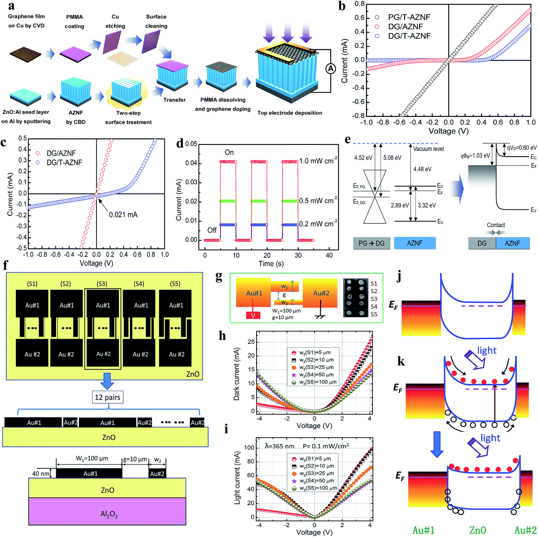 | ||
| Fig. 10 (a) Schematic representation of the processes involved in the fabrication of graphene/AZNF PD. (b and c) I–V characteristics of graphene/AZNF PDs in dark and UV conditions. (d) Cyclic photoresponses of the DG/T-AZNF PD at zero bias voltage under different UV illumination intensities (0.2 to 1 mW cm−2). (e) Schematic illustration of the energy band diagram of the DG/AZNF Schottky junction. Reproduced with permission from ref. 187 Copyright 2017 American Chemical Society. Asymmetric Schottky junctions: (f) schematic diagram of ZnO self-powered PDs having asymmetric electrodes. (g) Schematic demonstration of the photoresponse measurement configuration (left schematic) and the optical image of the PDs with different electrode dimensions (right image). (h and i) I–V characteristics in both the absence and presence of UV illumination (365 nm). (j and k) Energy band diagrams of the PD in dark and UV illumination conditions at zero bias voltage. Reproduced with permission from ref. 188 Copyright 2014 Royal Society of Chemistry. | ||
Likewise, asymmetric Schottky junction-based self-powered UV PDs were reported by Chen and co-authors, where Au asymmetric electrodes were introduced to control the charge carrier transportation.188Fig. 10f shows schematic diagrams of the fabricated devices having different asymmetric Au electrode width ratios (width of wide fingers:width of narrow fingers), including 20:1 (S1), 10:1 (S2), 4:1 (S3), 2:1 (S4) and 1:1 (S5). Fig. 10g shows the photoconduction measurement configuration (left schematic) and optical image of the respective PDs (right image). The I–V characteristics of the PDs with and without UV illumination are depicted in Fig. 10h and i, confirming their rectifying behaviors. It can be observed from the results that with an increase in asymmetric ratio from S5 to S1, the I–V asymmetricity between the positive and negative voltage increased due to the increase in the asymmetric Schottky barrier width in both the absence and presence of UV illumination. The authors reported efficient self-powered photoconduction responses in the S1 PD, which were ∼20 mA W−1 responsivity, ∼710 ns response time and ∼4 ms recovery time, where the S3–S5 PDs showed relatively negligible self-powered responses due to their nearly back-to-back symmetric Schottky barrier width. The self-powered working mechanism of S1 can be explained by the energy band diagrams before and after UV illumination (Fig. 10j and k, respectively). Upon exposure to UV illumination, electrons and holes are photogenerated (Fig. 10k, top schematic) and due to the asymmetrical width of the Au electrodes, an asymmetric electric potential distribution occurs, where the generated carriers become separated and transported by the potentials at zero bias voltage (Fig. 10k, bottom schematic).
Similar to that in piezo-phototronic-based conventional UV PDs, the piezo-phototronic effect of ZnO was coupled to enhance the performance of self-powered PDs. The generated piezopotentials across ZnO allow the separation and transportation of photogenerated electrons and holes, which boost the self-powered photoconduction of PDs. A ZnO/Au Schottky junction-based self-powered UV PD was explored by Zhang's group,189 where its self-powered photodetection performance was improved by applying an external strain. Fig. 11a depicts the optical image (top) and schematic representation of the fabricated ZnO/Au PD on a flexible polystyrene substrate. As shown in Fig. 11b, the typical I–V characteristics (in linear and log scales) confirmed the rectifying barrier between ZnO and Au, having an ideality factor of about 3.04. It was reported that with an increase in strain from 0 to 0.580%, the self-powered photoconduction of the PD increased due to the increase in piezopotential, as depicted in Fig. 11c (cyclic photoresponses at different tensile strains), where Fig. 11d illustrates the photocurrent versus strain plot. At an applied tensile strain of 0.580%, nearly 440% enhancement in the photocurrent and five times improvement in sensitivity were measured compared to that with zero strain (Fig. 11e). The enhanced photoconduction of the PD under external tensile strain can be explained from the schematic shown in Fig. 11f (device schematic and bend diagram under tensile strain). Under an external tensile strain, enhancement and expansion of the built-in field occur at the ZnO/Au interface, which directly participates in the photoexcited separation and extraction to increase the self-powered photoconduction.
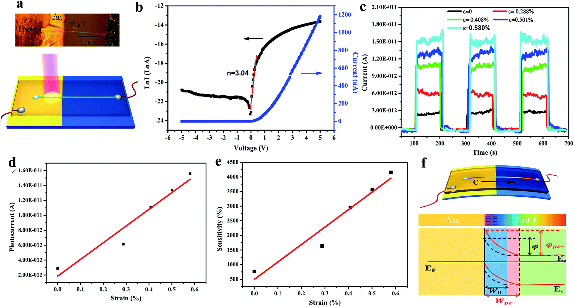 | ||
| Fig. 11 ZnO/Au Schottky junction: (a) optical image (top) and respective schematic of the ZnO/Au PD. (b and c) I–V characteristics (linear and log scales) and cyclic photoresponses at different tensile strains applied on the PD, respectively. (d and e) Photocurrent and sensitivity plots with respect to applied tensile strain, respectively. (f) Device schematic (top schematic) and the respective energy band diagram (bottom schematic) under tensile strain. Solid red and dotted black curves represent the energy band diagrams with and without tensile strain. W and φ represent the depletion region width and Schottky barrier height, respectively. Reproduced with permission from ref. 189 Copyright 2014 American Chemical Society. | ||
3.2.2.1 Inorganic homojunction/heterojunction-based self-powered UV photodetectors. In a p–n junction self-powered UV PDs, the generation of a built-in electric field occurs due to spontaneous electron and hole diffusion. The generated internal built-in electric field at the p–n junction interface is beneficial for the separation and transportation of photogenerated electrons and holes under UV illumination in the absence of an external driving force. Hence, the overall self-powered photoconduction is determined by the generated internal built-in electric field. Fig. 12a shows the SEM image of the n-ZnO NW/p-GaN junction self-powered UV PD reported by Bie and coauthors.190 The typical I–V profiles (Fig. 12b) of the PD in the dark and UV (325 nm) states confirm its rectifying behavior, having a threshold voltage of ∼3 V, open-circuit voltage of ∼2.7 V and short-circuit current of ∼2 μA. Upon exposure to UV illumination, the current of the PD increased from ∼1 pA to 2 μA at zero bias voltage due to the photovoltaic effect. Fig. 12c depicts the cyclic photoresponses of the PD measured with UV illumination turned on and off periodically at zero bias voltage, where an outstanding sensitivity ∼106 together with a much faster photodetection speed of ∼20 μs response time and ∼219 μs recovery time were reported by the authors. Zhang's group fabricated a p-NiO/n-ZnO NRs self-powered UV PD (Fig. 12d, device schematic).191 A significant enhancement in the current was observed upon exposure to UV illumination (355 nm) at zero bias voltage (Fig. 12e, I–V characteristics in both the dark and UV states) and Fig. 12f shows its photoresponses at different UV illumination intensities in the absence of a bias voltage. The authors measured a reasonable photodetection speed with a response time of 0.23 s and recovery time of 0.21 s, together with a maximum responsivity of 0.44 mA W−1 at the UV illumination intensity of 0.4 mW cm−2 in the absence of an external bias voltage. Likewise, different ZnO p–n junctions such as p-CuSCN/n-ZnO NWs,192 p-ZnO:(Li,N)/n-ZnO homojunction,193 p-Se/n-ZnO hybrid structure,194 Te/TiO2 and Te/ZnO heterojunctions195 devices have been explored for self-powered UV PD application.
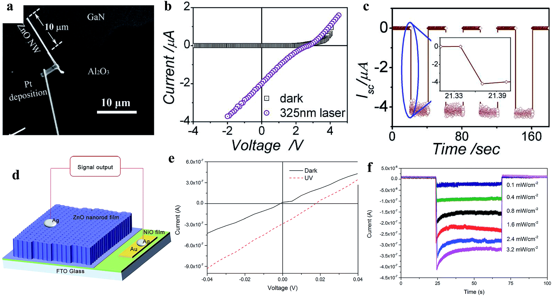 | ||
| Fig. 12 ZnO/GaN junction self-powered PD: (a and b) SEM image of n-ZnO NW/p-GaN junction and the respective I–V profiles under dark and UV illumination conditions, respectively. (c) Cyclic short circuit current–time response of the PD in the absence of a bias voltage with a 325 nm laser turned on and off repeatedly. Reproduced with permission from ref. 190 Copyright 2011 WILEY-VCH. p-NiO/n-ZnO NRs junction: (d and e) device schematic and I–V profiles before and after exposure to UV light. (f) Variation in current with respect to UV illumination intensity at zero bias condition. Reproduced with permission from ref. 191 Copyright 2015 Royal Society of Chemistry. | ||
Recently, the development of transparent and self-powered UV PDs has been given significant attention in the scientific community, where Fang group's has been focusing on the fabrication of transparent and self-powered UV PDs. For instance, a homojunction of n-type ZnO and Ag-doped p-type ZnO nanofibers was reported for application in transparent and self-powered UV PDs.196Fig. 13a shows the simulated electric field distribution around the three electrode collectors applied for the alignment of the as-prepared nanofibers (left image) and the electrospinning system for nanofiber synthesis (right image). The optical images of the aligned nanofibers and as-fabricated transparent and self-powered UV PDs are depicted in Fig. 13b and c, respectively. The authors observed that the doping of Ag on ZnO not only reduced the photoresponse time but also transformed the n-type ZnO to p-type conductivity for the direct fabrication of homojunction-based self-powered PDs, where Fig. 13d shows the p–n junction type I–V characteristics in both the absence and presence of UV illumination (360 nm, 2.5 mW cm−2). It can be observed from the I–V characteristics that the fabricated PD exhibited a clear rectification nature and photovoltaic effect with an open circuit voltage of 0.55 V, short circuit current of 5.0 × 10⁻¹⁰ A, and sensitivity of nearly 2.5 × 10⁴ at zero bias voltage condition, which imply that the fabricated PD can be operated in the absence of an external bias voltage (Fig. 13e depicts the cyclic photoresponse at zero bias). Moreover, the authors reported a response time and recovery time of 3.90 s and 4.71 s, respectively, and responsivity of nearly 1 mA W−1 in the absence of an external bias voltage.
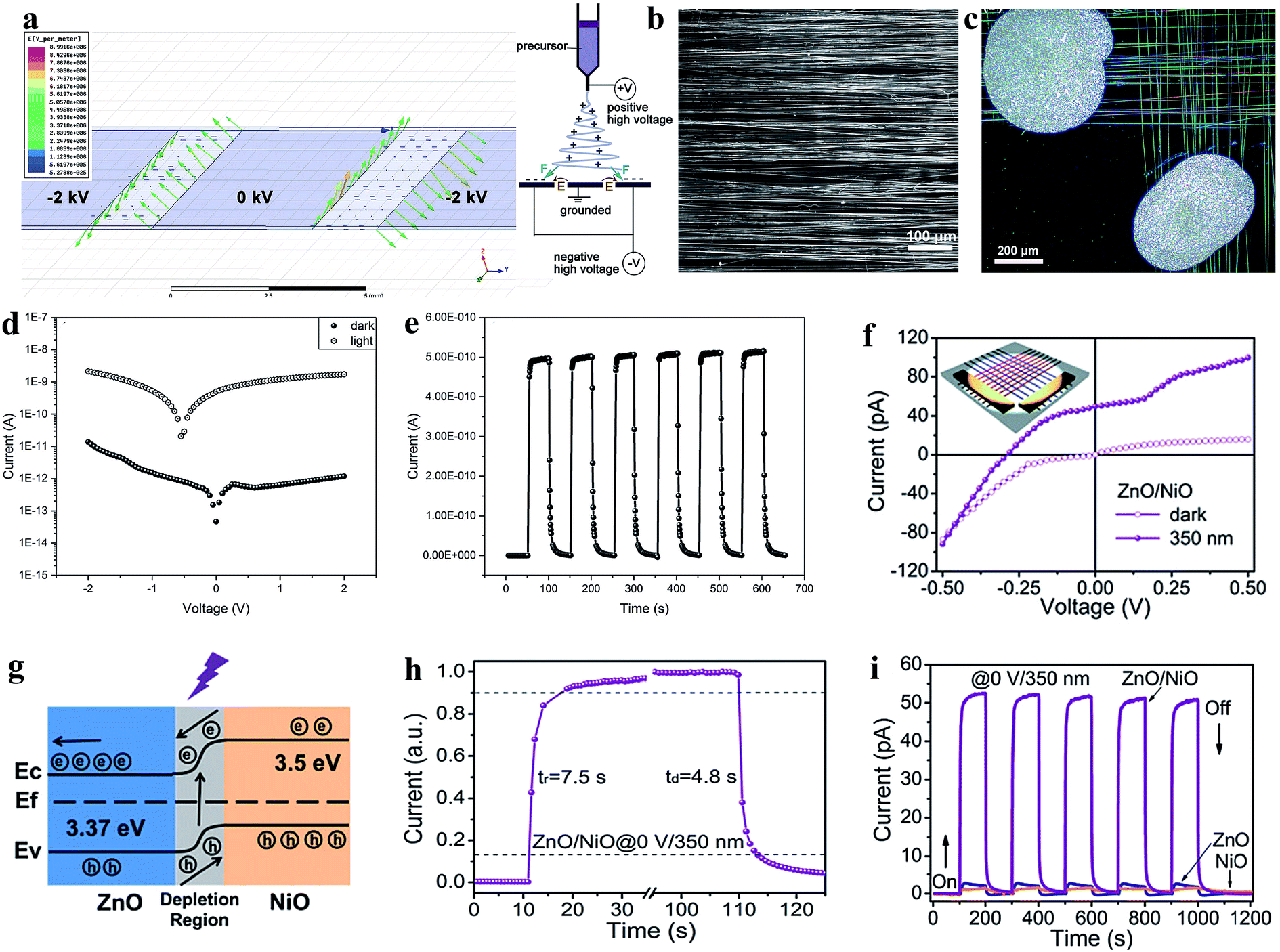 | ||
| Fig. 13 Transparent and self-powered UV PDs: (a) left image shows the electric field distribution around the three electrode collector applied for nanofiber alignment and schematic diagram of electrospinning setup (right schematic). (b and c) Optical images of aligned nanofibers and the as-fabricated transparent p–n homojunction (n-type ZnO nanofibers and Ag-doped p-type ZnO) based UV PD. (d) I–V responses in both the absence and presence of UV light (360 nm, 2.5 mW cm−2). (e) Cyclic photoresponses in the absence of a bias voltage. Reproduced with permission from ref. 196 Copyright 2018 WILEY-VCH. (f) I–V characteristics both in the absence and presence of UV light and inset depicts a schematic representation of the respective ZnO/NiO heterojunction-based PD. (g and h) Energy band diagram of the PD with exposure to UV light and estimation of its response time and recovery time. (i) Cyclic photoresponses of the UV PDs: pristine ZnO, pristine NiO and ZnO/NiO heterojunction in the absence of a bias voltage. Reproduced with permission from ref. 197 Copyright 2019 The Royal Society of Chemistry. | ||
Likewise, the same group extended their study to the fabrication of transparent and self-powered UV PDs based on ZnO/NiO heterojunction nanofiber arrays.197 As shown in Fig. 13f, the I–V profiles of the ZnO/NiO heterojunction PD (inset image) in the dark and UV states imply rectification p–n junction behavior with a photovoltaic effect, where the respective energy band diagram is depicted in Fig. 13g. Under exposure to UV illumination (350 nm, 0.753 mW cm−2), the photogenerated electrons are driven towards ZnO; whereas, the holes move to NiO due to the internal built-in electric field at the interface to generate a photocurrent of 50 pA in the absence of an external bias. Fig. 13h shows the estimation of response time and recovery time of the transparent and self-powered UV PDs, which are around 7.5 s and 4.8 s, respectively. In addition, the PD showed a maximum responsivity of 0.415 mA W−1 at 0 V bias voltage condition. However, negligible photoresponses of pristine ZnO and NiO were observed when the photoresponses were measured in absence of an external bias voltage (Fig. 13i), which implies that the internal built-in electric field needs to drive the photogenerated electrons and holes internally for self-powered photoconduction.
3.2.2.2 Inorganic–organic heterostructure-based self-powered UV photodetectors. Similar to inorganic homojunctions/heterojunction p–n type self-powered PDs, the organic–inorganic heterojunctions that form p–n junctions can also be operated without an external bias, where the generated internal electric field due to Fermi energy level alignments separate and drive the photogeneration of charges. This type of PD mainly comprises organic and inorganic semiconductors, where the inorganic semiconductor acts as the light sensitive material, while the organic semiconductor provides the direct charge conduction channel. Therefore, organic semiconductors can be used for either electron or hole transportation, depending on the type of inorganic semiconductor. Due to the n-type semiconducting behavior of ZnO, p-type organic semiconductors such as PEDOT:PSS, Spiro-MeOTAD, and P3HT are preferable for the generation of an internal built-in electric field.
As illustrated in Fig. 14a (device schematic), we fabricated a ZnO NR and PEDOT:PSS-based self-powered UV PD,198 where properties of the ZnO were altered by doping chlorine (Cl) (Cl:ZnO) for better light trapping probability and PEDOT:PSS for efficient hole transportation efficiency by introducing dimethyl sulfoxide (DMSO-PEDOT:PSS). A much better self-powered photoresponse was observed in the Cl-ZnO NRs/DMSO-PEDOT:PSS PD (#4) as compared to that of ZnO NRs/PEDOT:PSS (#1), Cl-ZnO NRs/PEDOT:PSS (#2) and ZnO NRs/DMSO-PEDOT:PSS (#3) (Fig. 14b, cyclic photoresponses). Fig. 14c depicts the energy band diagram of Cl-ZnO NRs/PEDOT:PSS upon exposure to UV illumination, where the photogenerated electrons migrate to the ITO electrode and holes to PEDOT:PSS and then Ag electrode for self-powered photoconduction due to the built-in potentials. Cl doping in the ZnO NRs not only enhanced the charge carrier density, but also enhanced the surface roughness of the NRs, and hence increased the light trapping probability upon UV illumination (Fig. 14d and e shows the simulated electric field distributions on the smooth ZnO NR surface and rough Cl-ZnO NR surface, respectively). Fig. 14f shows the light harvesting efficiency (LHE = 100% − transmission% − reflection%) plots with respect to light wavelength (350 to 800 nm) of the ZnO NRs and Cl-ZnO NRs, which confirmed the capture of more photons on the rough surfaces of the Cl-ZnO NRs. At the UV illumination intensity of 3 mW cm−2 (365 nm), the measured self-generated photoresponses of the Cl-ZnO NRs/DMSO-PEDOT:PSS PDs were 300 nA (response current), 0.80 mA W−1 (responsivity), 1.12 × 10¹⁰ Jones (specific detectivity), 30 ms (response time) and 32 ms (recovery time).
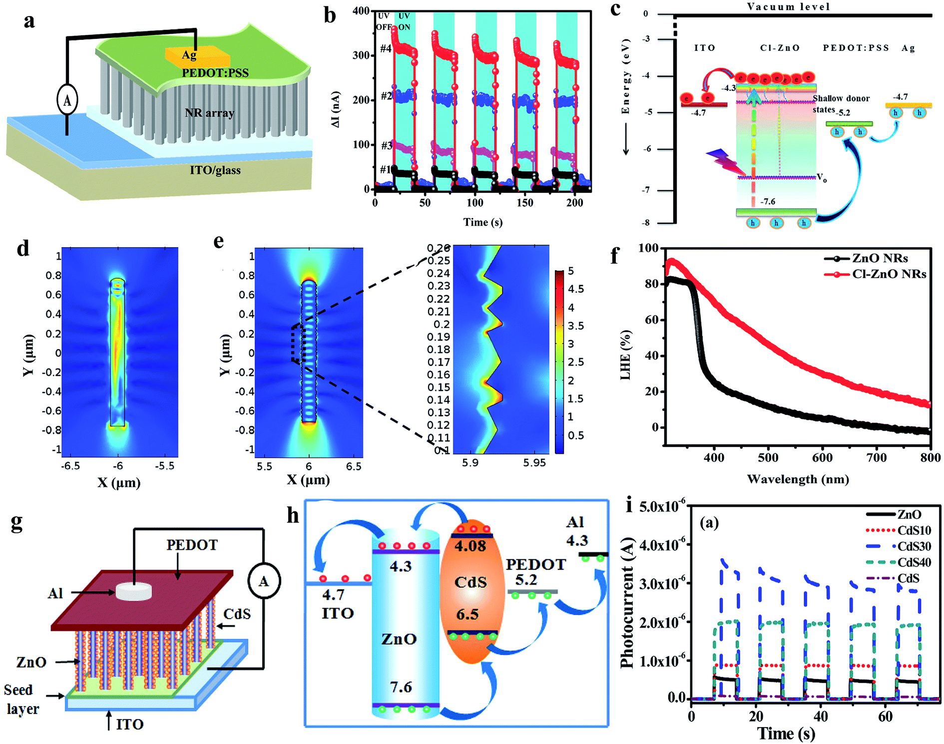 | ||
| Fig. 14 ZnO NRs and PEDOT:PSS heterostructure: (a) schematic illustration of the self-powered UV PD. (b) Cyclic photoresponses of the PDs (#1: ZnO NRs/PEDOT:PSS, #2: Cl-ZnO NRs/PEDOT:PSS, #3: ZnO NRs/DMSO-PEDOT:PSS and #4: Cl-ZnO NRs/DMSO-PEDOT:PSS PDs) under UV turned off and on repeatedly at zero bias voltage. (c) Schematic illustration of energy band diagram of Cl-ZnO NRs/PEDOT:PSS PD. (d and e) 2D simulated electric field distribution in ZnO NRs and Cl-doped ZnO NR, respectively. (f) LHE of pristine ZnO NRs and Cl-ZnO NRs. Reproduced with permission from ref. 198 Copyright 2017 Royal Society of Chemistry. ZnO@CdS/PEDOT:PSS heterostructure: (g and h) device schematic and energy band diagram upon exposure to light. (i) Cyclic photoresponses under UV off and on states at zero bias voltage. Reproduced with permission from ref. 199 Copyright 2015 American Chemical Society. | ||
Likewise, Basak's group fabricated a ZnO@CdS core–shell NR and PEDOT:PSS-based self-powered PD, as depicted in Fig. 14g (device schematic).199 The energy band diagram of the respective PD is shown in Fig. 14h, illustrating the migration of photogenerated electrons from ZnO to ITO and holes to CdS then PEDOT:PSS and finally to the Al electrode upon exposure to UV illumination. The authors optimized the self-powered photoresponse by controlling the CdS coating times from 0 (ZnO NRs) to 40 times (CdS40), and it was found that the 30-times CdS (CdS30) coated ZnO NRs showed the maximum self-powered response due to the optimum UV absorption efficiency in the CdS@ZnO core–shell structure, and thereby increased sensitivity of 2.8 × 10³ compared to the pristine ZnO NRs of sensitivity of 90 at 1 mW cm−2 UV illumination intensity. Moreover, the as-reported PD displayed a faster photodetection speed of ∼20 ms response time and ∼40 ms recovery time. Furthermore, the authors extended the self-powered photoconduction measurement of the ZnO@CdS/PEDOT:PSS PD to visible light.
Moreover, we fabricated hydrogenated ZnO (H:ZnO) NFs and PEDOT:PSS heterostructure for application in self-powered UV PDs.47 It was found that the H:ZnO NFs PD showed much higher photoresponse (1000 nA of response current) compared to that of the hydrogenated ZnO NR- (400 nA response current) and pristine ZnO NR- (40 nA response current) based PDs due to the abundant charge carrier density after hydrogenation and efficient light capturing in NFs. A higher LHE (98%) in the NF structure at 300 nm wavelength was measured due to the higher light adsorption capacity in the cavity of the NFs compared to that in the NRs or planar seed layer, which was 84% and 30%, respectively. Thereby, the fabricated H:ZnO NFs/PEDOT:PSS PD displayed efficient photodetection performances, including responsivity of 2.65 mA W−1 and 5.25 × 10¹⁰ Jones specific detectivity at 3 mW cm−2 UV (365 nm) illumination intensity in the absence of any external driving force. In addition, a faster photodetection speed of 23 ms response time and 26 ms recovery time was measured in the self-powered PD.
To explore the piezo-phototronic effect of ZnO for self-powered photoresponse application, Zhang's group fabricated a ZnO and Spiro-MeOTAD (p–n) heterojunction-based self-powered UV PD and enhanced its self-powered photoresponse performance by applying an external strain.200 As expected, the photoconduction of the PD increased with an increase in tensile strain due to the increase in the barrier height of ZnO and Spiro-MeOTAD (positive piezopotential at the interface), resulting in the effective separation of photogenerated charges upon exposure to UV, thereby improving the self-generated photoconduction. Nearly a one-fold enhancement in photocurrent (1.64 × 10⁻⁷ A), responsivity (0.8 mA W−1) and specific detectivity (4.2 × 10⁹ Jones) was reported by the authors when a tensile strain of 0.753% was applied on the PD in the absence of an external bias voltage.
With the rapid development of ZnO-based self-powered UV PDs, it has been realized that under light illumination, a transient increase in temperature across the ZnO nanostructures occurs to generate a potential known as pyro-potential. The induced pyro-charges under UV introduce an additional current, which enhances the overall self-powered photodetection performance of ZnO PDs. The pyro-phototronic effect is a very fast and rapid phenomenon, which can be utilized for ultrafast photon detection applications.201,202 Recently, several reports on pyro-phototronic-based ZnO self-powered UV PDs have been published by various research groups. Among them, Wang's group widely applied this effect for ultrafast self-powered photodetection applications.203Fig. 15a and b show a schematic representation of the ZnO NWs/PEDOT:PSS self-powered PD and its respective cyclic photoresponse upon exposure to UV illumination (325 nm, 2.30 mW cm−2) in the on and off states repeatedly at zero bias voltage. The current–time profile of the PD was completely different from the conventional UV PDs, where four stages (I, II, III and IV) of photocurrent dynamic behavior were measured, as shown in the magnified graph of Fig. 15b. In stage I: under UV illumination, the photogenerated electrons and holes migrated to the respective electrodes (ITO and Ag) for photocurrent generation (Iphoto), and simultaneously, a rapid increase in temperature in the ZnO NWs occurred to generate pyroelectric polarization potentials, i.e. pyro-potentials across the ZnO NWs. The positive pyro-potentials appeared at the PEDOT:PSS side; whereas, negative at the ITO electrode side according to the c-axis alignment of ZnO NWs, which resulted in the generation of an additional spike current known as pyro-current (Ipyro). Therefore, the overall current of the PD in stage I can be expressed as I = Iphoto + Ipyro (Fig. 15c(i), schematic illustration of photoconduction at stage I). While the PD is under constant UV illumination, the temperature generation of the ZnO NWs remained almost unchanged and the pyroelectric effect disappeared in stage II (Fig. 15c(ii), I = Iphoto). When UV light is switched off, the photocurrent of the PD goes to zero (Iphoto = 0), but a rapid decrease in temperature takes place across ZnO NWs, which generates opposite distribution of pyro-potentials across the ZnO NWs for a reverse spike pyro-current (I = −Ipyro) in stage III (Fig. 15c(iii)). While the PD is under maintained in dark condition, the generated temperature under UV keeps constant and finally, pyro-current of the PD transforms to its original condition (I = Idark) as depicted in Fig. 15c(iv). This pyro-phototronic effect in ZnO increased with an increase in the UV radiation temperature (illumination intensity). Fig. 15d shows the variation in Ipyro+photo and Iphoto with UV illumination intensity, where nearly 350% enhancement (E = (Ipyro+photo − Iphoto)/Iphoto) in the photoresponse at 2.30 mW cm−2 was reported due to the photo-phototronic effect (inset in Fig. 15d). Likewise, Fig. 15e shows the corresponding responsivities of the Rpyro+photo and Rphoto of the PD, where 500% enhancement in these parameters was reported after considering the pyro-phototronic effect (inset in Fig. 15e).
 | ||
| Fig. 15 (a) Schematic diagram of PEDOT:PSS/ZnO heterojunction PD. (b) Cyclic responses of the PD upon exposure to UV light (325 nm, 2.30 mW cm−2) at zero bias voltage and magnified plot shows four-stage (I, II, III and IV) current response profile. (c) Schematic illustration of photoconduction of the PD at the stages of I, II, III and IV. (d and e) Pyro-phototronic effect-induced current, Ipyro+photo, and photocurrent, Iphoto, plots and corresponding responsivity (Rpyro+photo and Rphoto) plots with respect to UV illumination (325 nm) intensity. Inset plots depict calculated corresponding enhancements at different UV illumination intensities. Reproduced with permission from ref. 203 Copyright 2017 WILEY-VCH. Cl:ZnO NRs/PEDOT:PSS PD: (f and g) device schematic and current response of the Cl:ZnO NRs PD under UV illumination (365 nm, 3 mW cm−2) at zero bias voltage. (h) Photocurrent (Iph) and pyrocurrent (Ipy) profiles with respect to the charge carrier density of ZnO NRs. Reproduced with permission from ref. 204 Copyright 2018 Royal Society of Chemistry. | ||
Moreover, we tuned the pyro-phototronic effect of ZnO NRs by tuning the charge carrier density by doping halogen elements,204 and Fig. 15f and g depict the device schematic and photoresponse profile of the Cl:ZnO NRs/PEDOT:PSS-based self-powered PD, respectively. Interestingly, it was found that the pyro-phototronic response of the ZnO NRs increased with the charge carrier density, where an efficient photoresponse was observed in the Cl-doped ZnO (Cl:ZnO) NRs due to the highest charge carrier density, and Fig. 15h shows the similar transient current profile of the PD upon exposure to UV illumination in the absence of a bias voltage, where four stages in the current profile were observed due to the pyro-phototronic effect. The photocurrent (Iph) and pyrocurrent (Ipy) plots with respect to the charge carrier density of the ZnO NRs confirm the enhancement in the photoresponse behavior. At the carrier density of 3.23 × 109 cm−2 (pristine ZnO NRs) the observed photocurrent and pyrocurrent were ∼40 nA and ∼90 nA, which increased to 220 nA and 344 nA when the charge carriers density was 7 × 1010 cm−2 for the Cl:ZnO NRs, respectively. Likewise, various pyro-phototronic-based self-powered UV PDs have been reported by many groups, for instance, ZnO/perovskite heterostructures,205,206 ZnO/Ag Schottky junction,207 and ZnO NWs/SnS PD.208
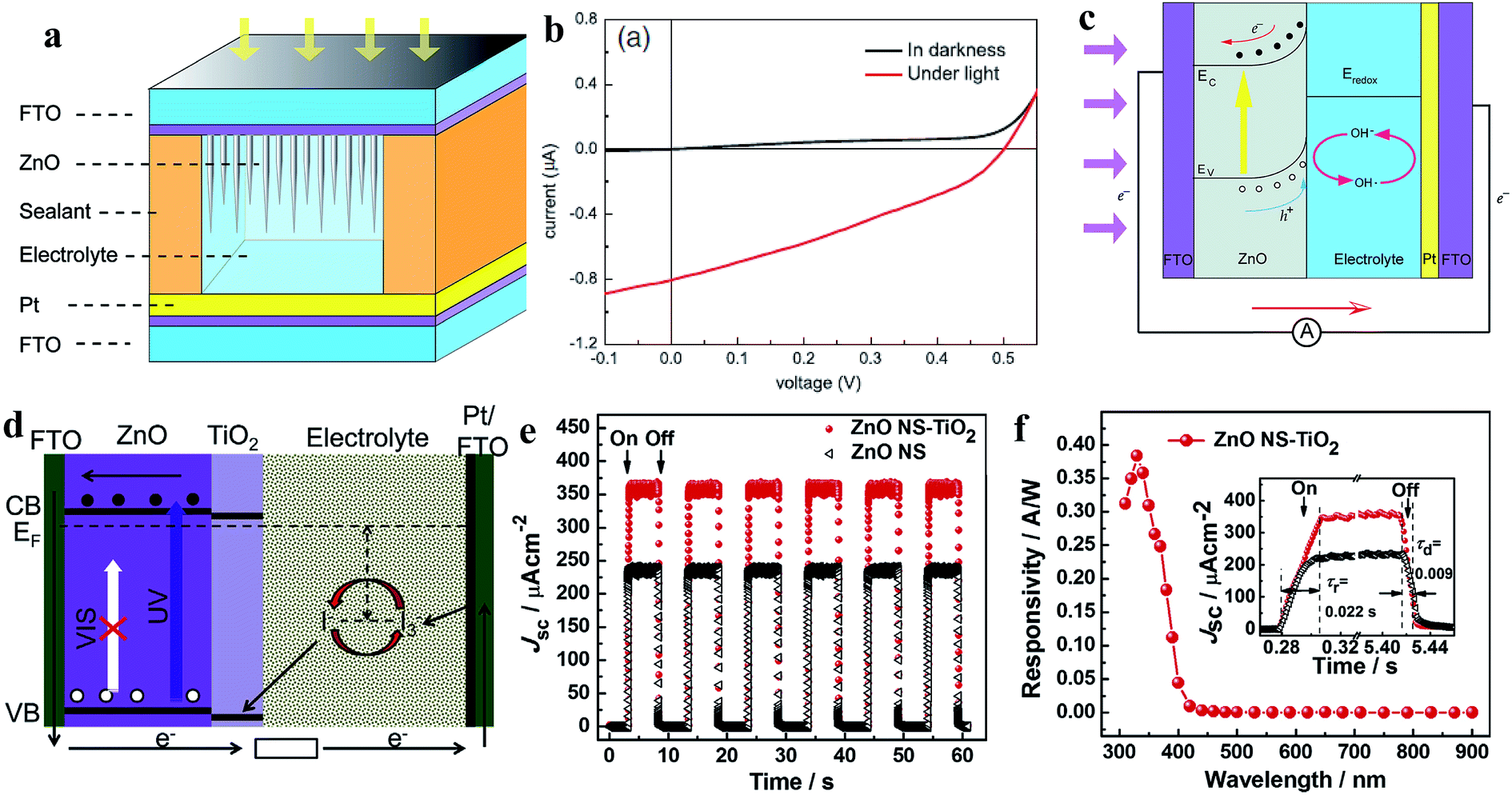 | ||
| Fig. 16 ZnO NN photoanode: (a) device schematic of ZnO NN photoanode-based PECC-type PD. (b and c) I–V profiles in dark and UV (365 nm, 1.25 mW cm−2) conditions and self-powered working mechanism under exposure to UV, respectively. Reproduced with permission from ref. 209 Copyright 2013 Springer. ZnO NSs-TiO2 core–shell photoanodes: (d) energy band diagram and working principle of the PD under exposure to UV irradiation. (e) Cyclic photoresponses of ZnO NSs-TiO2 core–shell photoanode- and ZnO NSs photoanode-based PDs upon exposure to UV light (365 nm, 20 mW cm−2) in the off and on states. (f) Spectral photoresponse and inset response/recovery time calculation of the PECC PD. Reproduced with permission from ref. 210 Copyright 2013 Elsevier. | ||
Xie's group fabricated TiO2-coated ZnO nanostrawberry (NS) (ZnO NS-TiO2) core–shell photoanodes for application in PECC-type self-powered UV PDs, as depicted in Fig. 16d (schematic of the energy band diagram under self-powered photoconduction).210 The photogenerated holes under UV illumination migrated to the TiO2/electrolyte interface for the reaction of h+ + I− → I3− due to the internal built-in electric field, while the photogenerated electrons were transported to the counter electrode through ZnO and the external circuit. Finally, the oxidized redox species were reduced at the counter electrode by electrons (I3− + e− → I−). The authors reported higher self-biased photoresponse behavior in the ZnO NS-TiO2 core–shell photoanode (357 mA cm−2) compared to the pristine ZnO NS photoanode (234 mA cm−2) due to the obvious generated built-in electric field at the ZnO and TiO2 interface (Fig. 16e, cyclic photoresponses at 365 nm and 20 mW cm−2 intensity). The ZnO NS-TiO2 core–shell photoanode-based PECC PD showed a sensitivity of ∼37900, maximum responsivity of ∼0.38 A W−1 at ∼330 nm together with a faster photodetection speed of ∼22 ms (response time) and ∼9 ms (recovery time) (Fig. 16f). Likewise, a ZnO NR photoanode, [Co(bpy)3]3+/2+ electrolyte, PEDOT/ITO counter electrode-based PECC,211 ZnO NR photoanode, iodine-free quasi solid-state electrolyte and Pt/FTO counter-based PECC212 were reported for self-powered photodetection. However, due to the involvement of liquid electrolytes, PECC PDs may have restricted applications.
With the constant efforts and research dedication by researchers, various ZnO nanostructure-based self-powered UV PDs have been reported, and Table 3 summarizes the photoresponse performances of the various reported ZnO nanostructures/heterostructure-based self-powered PDs.
| PD | UV light | Response current | Response time & recovery time | Sensitivity | Responsivity | Specific detectivity |
|---|---|---|---|---|---|---|
| H:VZnO NFs/PEDOT:PSS47 | 365 nm | 100 nA | 23 ms & 26 ms | — | 2.65 mA W−1 | 5.25 × 10¹⁰ Jones |
| Cl-ZnO NRs/DMSO-PEDOT:PSS198 | 365 nm | 300 nA | 30 ms & 32 ms | — | 0.80 mA W−1 | 1.12 × 10¹⁰ Jones |
| rGO-ZnO nanostructure213 | 334 nm | 20 nA | 0.2 s & 0.2 s | |||
| PEDOT:PSS/ZnO micro/NW214 | 325 nm | 1.2 nA | 1 s & 1 s | — | — | — |
| p-NiO/ZnO-NRs191 | 355 nm | 300 nA | 0.23 s & 0.21 s | ∼105 | 0.44 mA W−1 | — |
| Ag-ZnO NWs215 | 365 nm | 71 × 103 nA | 0.14 s & 0.52 s | |||
| Cl:ZnO NRs/PEDOT:PSS204 | 365 nm | 564 nA | 28 ms & 23 ms | — | 2.33 mA W−1 | 1.54 × 10¹⁰ Jones |
| n-Ga:ZnO/p-GaN140 | — | — | — | 3.2 × 10⁵ | 230 mA W−1 | 2.32 × 10¹² Jones |
| n-ZnO/i-MgO/p-GaN216 | 365 nm | — | 3.2 s & 3.84 s | — | 320 mA W−1 | 8.0 × 10¹² Jones |
| ZnO/GaN190 | 0.02 ms & 0.22 ms | ∼132 mA W−1 | — | |||
| n-ZnO/p-CuSCN217 | 325 nm | — | 0.5 μs & 6.7 μs | — | 7.5 mA W−1 | — |
| n-ZnO/p-NiO191 | 355 nm | — | 0.23 s & 0.21 s | — | 0.44 mA W−1 | — |
| Au#1-ZnO-Au#2 (ref. 218) | 365 nm | — | 710 ns & 4 μs | — | 20 mA W−1 | — |
| p-ZnO(Li,N)/n-ZnO193 | — | — | — | — | 0.018 mA W−1 | — |
| p-GaN/n-ZnO219 | 374 nm | — | — | — | 0.001 mA W−1 | 1.41 × 10⁸ Jones |
| Au/MgZnO220 | — | — | — | — | 0.059 mA W−1 | — |
| Au-ZnO(I)/ZnO(n)/In221 | — | — | — | — | 0.03 mA W−1 | — |
| Au/MgO/MgZnO222 | 366 nm | — | — | — | 11 mA W−1 | — |
| Pt/ZnO NWs/Al223 | 355 nm | — | 81 ms & 95 ms | 3.1 × 10⁴ | — | — |
| ZnO NWs/CuSCN192 | 370 nm | — | — | — | 0.02 A W−1 | — |
| n-ZnO/p-GaN190 | 325 nm | ∼2 μA | 20 μs & 219 μs | — | — | — |
| Sb-doped ZnO nanobelt/Au46 | 325 nm | 22 nA | 100 ms & 100 ms | 23 | — | — |
| ZnO/Spiro-MeOTAD200 | 365 nm | ∼0.2 μA | 0.16 s & 0.20 s | — | 0.8 mA W−1 | 4.2 × 10⁹ Jones |
| n-ZnO/CdS/p-GaN224 | 365 nm | — | 0.35 s & 0.35 s | — | 176 mA W−1 | 2.5 × 10¹² Jones |
| Graphene/ZnO:Al NRs187 | 365 nm | — | 37 μs & 330 μs | 100 | 39 mA W−1 | — |
| p-CuSCN/n-ZnO NRs175 | 365 nm | — | 3.20 s & 3.84 s | — | 22.5 mA W−1 | — |
| ZnO/Ga2O3 (ref. 225) | 251 nm | ∼6 nA | 100 μs & 900 μs | — | 9.7 mA W−1 | 6.29 × 10¹² Jones |
| CuSCN/ZnO217 | 350 nm | — | 500 ns & 6.7 μs | — | 7.5 mA W−1 | — |
| Polyaniline/MgZnO226 | 250 nm | — | 0.3 s & 0.3 s | ∼104 | 0.16 mA W−1 | 1.5 × 10¹¹ Jones |
| ZnO(N)-Spiro-MeOTAD227 | 390 nm | — | 200 μs & 950 μs | 300 | 17 mA W−1 | — |
| ZnO & PEDOT/ITO PECC211 | 365 nm | — | 0.2 s & 0.2 s | — | — | — |
| ZnO & Pt/FTO PECC228 | 365 nm | ∼30 nA | 0.06 s & 0.06 s | — | — | — |
| ZnO & Pt/FTO PECC229 | — | — | 0.07 s & 0.07 s | 102 | — | — |
| ZnO & Pt/FTO PECC215 | 365 nm | 21.61 μA cm−2 | 0.15 s & 0.5 s | 32.32 | 370 mA W−1 | — |
| ZnO NRs & Pt/FTO PECC212 | 365 nm | ∼140 μA | 0.09 s & 0.31 s | ∼534 | 2.33 A W−1 | — |
| ZnO NSe-TiO2 & Pt/FTO PECC210 | 365 nm | — | 0.022 s & 0.009 s | 37900 |
∼0.38 A W−1 | — |
| ZnO NNs & Pt/FTO PECC209 | 365 nm | — | 0.1 s & 0.1 s | — | 0.022 A W−1 | — |
| ZnO/Au189 | 325 nm | — | 0.1 s & 0.1 s | ∼4000 | — | — |
| ZnO/Ag207 | 325 nm | — | 4.5 ms & 3.5 ms | — | — | 2.7 × 10⁹ Jones |
| ZnO/perovskite-heterostructure206 | 325 nm | — | 53 μs & 63 μs | — | 26.7 mA W−1 | 4.0 × 10¹⁰ Jones |
| ZnO/perovskite205 | 325 nm | ∼1 μA | — | — | — | — |
| p-ZnO:(As)/n-ZnO137 | 370 nm | — | 30 ms & 50 ms | 106 | — | — |
| p-CuSCN/n-ZnO192 | 370 nm | — | — | 20 mA W−1 | — | |
| p-GaN/n-ZnO230 | 358 nm | — | — | — | 0.68 mA W−1 | — |
| n-ZnO/p-PANI/n-ZnO231 | 365 nm | 0.5 μA | — | 1.68 × 10⁵ | — | — |
| Graphene/ZnO187 | 380 nm | — | 37 μs & 330 μs | 100 | ∼40 mA W−1 | — |
4. Conclusions and perspectives
This article reviewed the recent development in ZnO nanostructure/heterostructure-based UV PDs from the conventional to self-powered device designs. The intrinsic ZnO photoresponse mechanism and various potential nanostructures ranging from 0D to 3D were briefly introduced. Both the conventional and self-powered ZnO-based UV PDs were precisely categorized based on device structure and working mechanism, where recently introduced novel phenomena such as piezo-electric, pyro-electric and plasmonic effects for efficient photoconduction were discussed carefully. Moreover, there are still a couple of that issues need to be investigated in the development of next-generation conventional and self-powered UV PDs as follows:4.1 Improvement of photodetection speed of UV photodetectors
It can be observed from the literature (Table 2) that the photodetection speed (response time and recovery time) of conventional ZnO-based UV PDs varies from a few hundred seconds to milliseconds. It is important to note that the existence of native defects such as O and Zn vacancies and the excess of Zn and O atoms in ZnO behave like trapping centers for charge careers to extend the recombination and charge carrier generation time under exposure to UV illumination. Therefore, it is very important to reduce the native defects in ZnO nanostructures for efficient photoconduction.4.2 Reduction of lattice mismatch of heterostructures
It is well known that homojunction/heterojunction-based ZnO PDs show a higher-photoresponse performance than their bare counterparts due to the internal built-in electric at their interface. Sometimes, heterojunction-based ZnO PDs show a slower response time and recovery time during photoconduction, which is mainly due to the defect states present at the junction interface originating mainly due to lattice mismatch at the interface of heterostructures. Therefore, to achieve a desirable photoresponse in homojunction- or heterojunction-based UV PDs, the lattice mismatch at the interface needs to be reduced.4.3 Improvement of responsivities of self-powered photodetectors
It is necessary to highlight that even though there has been significant research effort in the development of ZnO self-powered PDs with rapid photodetection speed and superior sensitivity, the responsivities of the reported self-powered ZnO PDs are still limited, which are relatively lower than that of conventional ZnO UV PDs (Tables 2 and 3). As discussed earlier, the built-in electric fields at the junctions/interfaces of self-powered UV PDs define their photoresponse performance in terms of both response current and responsivity. Thus, to enhance the responsivity of self-powered PDs, the strength of the built-in electric field and the photoconductivity of photoactive materials for faster conduction need to increase for the realization of their direct practical applications.4.4 Optimization of surface roughness of nanomaterials
ZnO nanostructure morphologies play a crucial role in the light trapping effect, which determines the electron and hole pair generation efficiency. Therefore, the optimum surface roughness on ZnO nanostructures needs to be considered to increase the surface-induced photocharge effects. In addition, the carrier concentration of ZnO nanomaterials needs to be improved for optimum charge conduction.4.5 Development of on-chip and planar wearable UV photodetectors
Nowadays, the rapid increase in the demands of portable modern electronic devices have made it necessary for on-chip, small size, lightweight with high-performance miniaturized UV PDs. Therefore, to fulfill these requirements, wearable high-performance UV PDs232 and silicon-compatible-based conventional/self-powered UV PDs for on-chip and planar technology233,234 need to be focused on in upcoming research.Conflicts of interest
There are no conflicts to declare.Acknowledgements
BDB would like to acknowledge the support from the Royal Society, grant number of NIF\R1\181656.References
- F. Teng, K. Hu, W. Ouyang and X. Fang, Adv. Mater., 2018, 30, 1706262 CrossRef PubMed.
- S. Bhandari, D. Mondal, S. K. Nataraj and R. G. Balakrishna, Nanoscale Adv., 2019, 1, 913 RSC.
- W. Ouyang, F. Teng, J. -H. He and X. Fang, Adv. Funct. Mater., 2019, 29, 1807672 CrossRef.
- H. Chen, L. Su, M. Jiang and X. Fang, Adv. Funct. Mater., 2017, 27, 1704181 CrossRef.
- J. Zhou, L. Chen, Y. Wang, Y. He, X. Pan and E. Xie, Nanoscale, 2016, 8, 50 RSC.
- Y. Zhang, W. Xu, X. Xu, J. Cai, W. Yang and X. Fang, J. Phys. Chem. Lett., 2019, 10, 836 CrossRef CAS PubMed.
- T. Tong, S. Wang, J. Zhao, B. Cheng, Y. Xiao and S. Lei, Nanoscale Horiz., 2019, 4, 138 RSC.
- L. Peng, L. Hu and X. Fang, Adv. Mater., 2013, 25, 5321 CrossRef CAS PubMed.
- L. Su, W. Yang, J. Cai, H. Chen and X. Fang, Small, 2017, 13, 1701687 CrossRef PubMed.
- H. Chen, K. Liu, L. Hu, A. A. Al-Ghamdi and X. Fang, Mater. Today, 2015, 18, 493 CrossRef CAS.
- T. Zhai, X. Fang, M. Liao, X. Xu, H. Zeng, B. Yoshio and D. Golberg, Sensors, 2009, 9, 6504 CrossRef CAS PubMed.
- http://en.wikipedia.org/wiki/Sunlight# .
- E. Monroy, F. Omnès and F. Calle, Semicond. Sci. Technol., 2003, 18, R33 CrossRef CAS.
- X. Li, M. Rui, J. Song, Z. Shen and H. Zeng, Adv. Funct. Mater., 2015, 25, 4929 CrossRef CAS.
- K. Thorkelsson, P. Bai and T. Xu, Nano Today, 2015, 10, 48 CrossRef CAS.
- Y. Guo, K. Xu, C. Wu, J. Zhao and Y. Xie, Chem. Soc. Rev., 2015, 44, 637 RSC.
- J. Lahnemann, M. D. Hertog, P. Hille, M. d. l. Mata, T. Fournier, J. Schörmann, J. Arbiol, M. Eickhoff and E. Monroy, Nano Lett., 2016, 16, 3260 CrossRef CAS PubMed.
- X. Fang, Y. Bando, M. Liao, U. K. Gautam, C. Zhi, B. Dierre, B. Liu, T. Zhai, T. Sekiguchi, Y. Koide and D. Golberg, Adv. Mater., 2009, 21, 2034 CrossRef CAS.
- C. Zhang, Y. Xie, H. Deng, T. Tumlin, C. Zhang, J. -W. Su, P. Yu and J. Lin, Small, 2017, 13, 1604197 CrossRef PubMed.
- A. Aldalbahi, E. Li, M. Rivera, R. Velazquez, T. Altalhi, X. Peng and P. X. Feng, Sci. Rep., 2016, 6, 23457 CrossRef CAS PubMed.
- E. Oksenberg, R. Popovitz-Biro, K. Rechav and E. Joselevich, Adv. Mater., 2015, 27, 3999 CrossRef CAS PubMed.
- M. Shaygan, K. Davami, B. Jin, T. Gemming, J.-S. Lee and M. Meyyappan, J. Mater. Chem. C, 2016, 4, 2040 RSC.
- J. Yao, Z. Deng, Z. Zheng and G. Yang, ACS Appl. Mater. Interfaces, 2016, 8, 20872 CrossRef CAS PubMed.
- P. Zhou, C. Chen, X. Wang, B. Hu and H. San, Sens. Actuators, A, 2018, 271, 389 CrossRef CAS.
- X. Fang, L. Hu, K. Huo, B. Gao, L. Zhao, M. Liao, P. K. Chu, Y. Bando and D. Golberg, Adv. Funct. Mater., 2011, 21, 3907 CrossRef CAS.
- R. A. Rani, A. S. Zoolfakar, N. S. Khairir, M. H. Mamat, S. Alrokayan, H. A. Khan and M. R. Mahmood, J. Mater. Sci.: Mater. Electron., 2018, 29, 16765 CrossRef.
- W. -Y. Kong, G. -A. Wu, K. -Y. Wang, T. -F. Zhang, Y. -F. Zou, D. -D. Wang and L. -B. Luo, Adv. Mater., 2016, 28, 10725 CrossRef CAS PubMed.
- X. Zhou, Q. Zhang, L. Gan, X. Li, H. Li, Y. Zhang, D. Golberg and T. Zhai, Adv. Funct. Mater., 2016, 26, 704 CrossRef CAS.
- L. Li, L. Gu, Z. Lou, Z. Fan and G. Shen, ACS Nano, 2017, 11, 4067 CrossRef CAS PubMed.
- Z. Wang, H. Wang, B. Liu, W. Qiu, J. Zhang, S. Ran, H. Huang, J. Xu, H. Han, D. Chen and G. Shen, ACS Nano, 2011, 5, 8412 CrossRef CAS PubMed.
- K. Liu, M. Sakurai and M. Aono, Sensors, 2010, 10, 8604 CrossRef CAS PubMed.
- L. Zheng, F. Teng, Z. Zhang, B. Zhao and X. Fang, J. Mater. Chem. C, 2016, 4, 10032 RSC.
- L. Hu, J. Yan, M. Liao, L. Wu and X. Fang, Small, 2011, 7, 1012 CrossRef CAS PubMed.
- H. Liu, Z. Zhang, L. Hu, N. Gao, L. Sang, M. Liao, R. Ma, F. Xu and X. Fang, Adv. Opt. Mater., 2014, 771 CrossRef CAS.
- Ü. Özgür, Y. I. Alivov, C. Liu, A. Teke, M. A. Reshchikov, S. Doğan, V. C. S. J. Avrutin, S.-J. Cho and H. Morkoç, J. Appl. Phys., 2005, 98, 11 CrossRef.
- Z. L. Wang, Mater. Sci. Eng., R, 2009, 64, 33 CrossRef.
- Z. L. Wang, J. Phys.: Condens. Matter, 2004, 16, R829 CrossRef CAS.
- Z. L. Wang, Adv. Mater., 2012, 24, 4632 CrossRef CAS PubMed.
- Z. Gao, J. Zhou, Y. Gu, P. Fei, Y. Hao, G. Bao and Z. L. Wang, J. Appl. Phys., 2009, 105, 113707 CrossRef PubMed.
- Y. Yang, W. Guo, K. C. Pradel, G. Zhu, Y. Zhou, Y. Zhang, Y. Hu, L. Lin and Z. L. Wang, Nano Lett., 2012, 12, 2833 CrossRef CAS PubMed.
- H. Kind, H. Yan, B. Messer, M. Law and P. Yang, Adv. Mater., 2002, 14, 158 CrossRef CAS.
- C. Soci, A. Zhang, B. Xiang, S. A. Dayeh, D. P. R. Aplin, J. Park, X. Y. Bao, Y.-H. Lo and D. Wang, Nano Lett., 2007, 7, 1003 CrossRef CAS PubMed.
- X. Liu, L. Gu, Q. Zhang, J. Wu, Y. Long and Z. Fan, Nat. Commun., 2014, 5, 4007 CrossRef CAS PubMed.
- G. Chai, O. Lupan, L. Chow and H. Heinrich, Sens. Actuators, A, 2009, 150, 184 CrossRef CAS.
- N. Chantarat, Y.-W. Chen, S.-Y. Chen and C.-C. Lin, Nanotechnology, 2009, 20, 395201 CrossRef CAS PubMed.
- Y. Yang, W. Guo, J. Qi, J. Zhao and Y. Zhang, Appl. Phys. Lett., 2010, 97, 223113 CrossRef.
- B. D. Boruah and A. Misra, ACS Appl. Mater. Interfaces, 2016, 8, 18182 CrossRef PubMed.
- Y. Jin, J. Wang, B. Sun, J. C. Blakesley and N. C. Greenham, Nano Lett., 2008, 8, 1649 CrossRef CAS PubMed.
- H. Y. Yang, D. I. Son, T. W. Kim, J. M. Lee and W. I. Park, Org. Electron., 2010, 11, 1313 CrossRef CAS.
- C. He, T. Sasaki, Y. Shimizu and N. Koshizaki, Appl. Surf. Sci., 2008, 254, 2196 CrossRef CAS.
- X. H. Zhang, Y. C. Liu, X. H. Wang, S. J. Chen, G. R. Wang, J. Y. Zhang, Y. M. Lu, D. Z. Shen and X. W. Fan, J. Phys.: Condens. Matter, 2005, 17, 3035 CrossRef CAS.
- M. H. Huang, Y. Wu, H. Feick, N. Tran, E. Weber and P. Yang, Adv. Mater., 2001, 13, 113 CrossRef CAS.
- L. Li, S. Pan, X. Dou, Y. Zhu, X. Huang, Y. Yang, G. Li and L. Zhang, J. Phys. Chem. C, 2007, 111, 7288 CrossRef CAS.
- J. L. Yang, S. J. An, W. I. Park, G. -C. Yi and W. Choi, Adv. Mater., 2004, 16, 1661 CrossRef CAS.
- L. Wang, X. Zhang, S. Zhao, G. Zhou, Y. Zhou and J. Qi, Appl. Phys. Lett., 2005, 86, 024108 CrossRef.
- J. -J. Wu and S. -C. Liu, Adv. Mater., 2002, 14, 215 CrossRef CAS.
- K.-F. Lin, H.-M. Cheng, H.-C. Hsu, L.-J. Lin and W.-F. Hsieh, Chem. Phys. Lett., 2005, 409, 208 CrossRef CAS.
- B. Liu and H. C. Zeng, J. Am. Chem. Soc., 2003, 125, 4430 CrossRef CAS PubMed.
- F. Lu, W. Cai and Y. Zhang, Adv. Funct. Mater., 2008, 18, 1047 CrossRef CAS.
- K. Raagulan, M. M. M. G. P. G. Mantilaka, G. T. D. Chandrakumara, U. G. M. Ekanayake, W. P. S. L. Wijesinghe, S. Ehanathan, R. M. G. Rajapakse, R. Braveenth and K. Y. Chai, Nanoscale Adv., 2019, 1, 481 RSC.
- M. K. Choudhary, J. Kataria, V. K. Bhardwaj and S. Sharma, Nanoscale Adv., 2019, 1, 1035 RSC.
- Y. Sun, N. G. Ndifor-Angwafor, D. J. Riley and M. N. R. Ashfold, Chem. Phys. Lett., 2006, 431, 352 CrossRef CAS.
- H. Lu, S. Wang, L. Zhao, J. Li, B. Dong and Z. Xu, J. Mater. Chem., 2011, 21, 4228 RSC.
- J. Liang, J. Liu, Q. Xie, S. Bai, W. Yu and Y. Qian, J. Phys. Chem. B, 2005, 109, 9463 CrossRef CAS PubMed.
- J. Joo, B. Y. Chow, M. Prakash, E. S. Boyden and J. M. Jacobson, Nat. Mater., 2011, 10, 596 CrossRef CAS PubMed.
- A. Manekkathodi, M. -Y. Lu, C. W. Wang and L. -J. Chen, Adv. Mater., 2010, 22, 4059 CrossRef CAS PubMed.
- S. Zhang, Y. Shen, H. Fang, S. Xu, J. Song and Z. L. Wang, J. Mater. Chem., 2010, 20, 10606 RSC.
- Y. Liang, N. Guo, L. Li, R. Li, G. Ji and S. Gan, RSC Adv., 2015, 5, 59887 RSC.
- T. Zhang, W. Dong, M. Keeter-Brewer, S. Konar, R. N. Njabon and Z. R. Tian, J. Am. Chem. Soc., 2006, 128, 10960 CrossRef CAS PubMed.
- X. Wang, W. Liu, J. Liu, F. Wang, J. Kong, S. Qiu, C. He and L. Luan, ACS Appl. Mater. Interfaces, 2012, 4, 817 CrossRef CAS PubMed.
- Y. Shi, C. Zhu, L. Wang, C. Zhao, W. Li, K. K. Fung, T. Ma, A. Hagfeldt and N. Wang, Chem. Mater., 2013, 25, 1000 CrossRef CAS.
- M. K. Gupta, J.-H. Lee, K. Y. Lee and S.-W. Kim, ACS Nano, 2013, 7, 8932 CrossRef CAS PubMed.
- H. V. Ngoc and D. J. Kang, Nanoscale, 2016, 8, 5059 RSC.
- M. R. Alenezi, S. J. Henley, N. G. Emerson and S. R. P. Silva, Nanoscale, 2014, 6, 235 RSC.
- T. Shinagawa, M. Watanabe, J.-I. Tani and M. Chigane, Cryst. Growth Des., 2017, 17, 3826 CrossRef CAS.
- N. Jalali, J. Briscoe, P. Woolliams, M. Stewart, P. M. Weaver, M. Cain and S. Dunn, J. Phys.: Conf. Ser., 2013, 476, 012131 CrossRef CAS.
- L. Zhang, Y. Ruan, Y. Liu and Y. Zhai, Cryst. Res. Technol., 2013, 48, 11 CrossRef CAS.
- Q. Yu, C. Yu, J. Wang, F. Guo, S. Gao, S. Jiao, H. Li, X. Zhang, X. Wang, H. Gao, H. Yang and L. Zhao, RSC Adv., 2013, 3, 16619 RSC.
- C. Lu, L. Qi, J. Yang, L. Tang, D. Zhang and J. Ma, Chem. Commun., 2006, 33, 3551 RSC.
- B. D. Boruah and A. Misra, RSC Adv., 2015, 5, 90838 RSC.
- W. Wu, X. Xiao, T. Peng and C. Jiang, Chem.–Asian J., 2010, 5, 315 CrossRef CAS PubMed.
- S. M. Majhi, P. Rai and Y.-T. Yu, ACS Appl. Mater. Interfaces, 2015, 7, 9462 CrossRef CAS PubMed.
- M. Chen, L. Hu, J. Xu, M. Liao, L. Wu and X. Fang, Small, 2011, 7, 2449 CAS.
- B. D. Boruah, D. B. Ferry, A. Mukherjee and A. Misra, Nanotechnology, 2015, 26, 235703 CrossRef PubMed.
- M. R. Alenezi, S. J. Henley and S. R. P. Silva, Sci. Rep., 2015, 5, 8516 CrossRef PubMed.
- X. H. Huang, Z. Y. Zhan, K. P. Pramoda, C. Zhang, L. X. Zheng and S. J. Chua, CrystEngComm, 2012, 14, 5163 RSC.
- L. W. Chang, Y. C. Sung, J. W. Yeh and H. C. Shih, J. Appl. Phys., 2011, 109, 074318 CrossRef.
- L. J. Luo, W. Tao, X. Y. Hu, T. Xiao, B. J. Heng, W. Huang, H. Wang, H. W. Han, Q. Jiang, J. B. Wang and Y. W. Tang, J. Power Sources, 2011, 196, 10518 CrossRef CAS.
- J. B. Cui, Y. C. Soo, T. P. Chen and U. J. Gibson, J. Phys. Chem. C, 2008, 112, 4475 CrossRef CAS.
- J. H. Lee, C. Y. Chou, Z. X. Bi, C. F. Tsai and H. Y. Wang, Nanotechnology, 2009, 20, 395704 CrossRef PubMed.
- A. Escobedo-Morales and U. Pal, Appl. Phys. Lett., 2008, 93, 193120 CrossRef.
- K. Mahmood, S. B. Park and H. J. Sung, J. Mater. Chem. C, 2013, 1, 3138 RSC.
- D. D. Wang, G. Z. Xing, M. Gao, L. L. Yang, J. H. Yang and T. Wu, J. Phys. Chem. C, 2011, 115, 22729 CrossRef CAS.
- N. Kouklin, Adv. Mater., 2008, 20, 2190 CrossRef CAS.
- H. M. Chiu and J. M. Wu, J. Mater. Chem. A, 2013, 1, 5524 RSC.
- C. L. Hsu, H. H. Li and T. J. Hsueh, ACS Appl. Mater. Interfaces, 2013, 5, 11142 CrossRef CAS PubMed.
- T.-H. Kao, J.-Y. Chen, C.-H. Chiu, C.-W. Huang and W.-W. Wu, Appl. Phys. Lett., 2014, 104, 111909 CrossRef.
- C.-L. Hsu and S.-J. Chang, Small, 2014, 10, 4562 CrossRef CAS PubMed.
- X. Y. Yang, A. Wolcott, G. M. Wang, A. Sobo, R. C. Fitzmorris, F. Qian, J. Z. Zhang and Y. Li, Nano Lett., 2009, 9, 2331 CrossRef CAS PubMed.
- M. P. Lu, J. Song, M. Y. Lu, M. T. Chen, Y. Gao, L. J. Chen and Z. L. Wang, Nano Lett., 2009, 9, 1223 CrossRef CAS PubMed.
- J. Y. Zhang, P. J. Li, H. Sun, X. Shen, T. S. Deng, K. T. Zhu, Q. F. Zhang and J. L. Wu, Appl. Phys. Lett., 2008, 93, 021116 CrossRef.
- M. Ahmad, C. F. Pan and J. Zhu, J. Mater. Chem., 2010, 20, 7169 RSC.
- W. T. Wan, J. Huang, L. P. Zhu, L. Hu, Z. Wen, L. W. Sun and Z. Z. Ye, CrystEngComm, 2013, 15, 7887 RSC.
- Y. W. Song, K. Kim, J. P. Ahn, G. E. Jang and S. Y. Lee, Nanotechnology, 2009, 20, 275606 CrossRef PubMed.
- N. Hongsith, C. Viriyaworasakul, P. Mangkomtong, N. Mangkorntong and S. Choopun, Ceram. Int., 2008, 34, 823 CrossRef CAS.
- O. D. Jayakumar, I. K. Gopalakrishnan and S. K. Kulshreshtha, Adv. Mater., 2006, 18, 1857 CrossRef CAS.
- H. N. Zhang, Z. Y. Li, W. Wang, C. Wang and L. Liu, J. Am. Ceram. Soc., 2010, 93, 142 CrossRef CAS.
- S. Ghosh, G. G. Khan, B. Das and K. Mandal, J. Appl. Phys., 2011, 109, 123927 CrossRef.
- S. Liang, H. Sheng, Y. Liu, Z. Huo, Y. Lu and H. Shen, J. Cryst. Growth, 2001, 225, 110 CrossRef CAS.
- D. Y. Guo, Z. P. Wu, Y. H. An, X. C. Guo, X. L. Chu, C. L. Sun, L. H. Li, P. G. Li and W. H. Tang, Appl. Phys. Lett., 2014, 105, 023507 CrossRef.
- R. Tang, S. Han, F. Teng, K. Hu, Z. Zhang, M. Hu and X. Fang, Adv. Sci., 2018, 5, 1700334 CrossRef PubMed.
- F. Teng, L. Zheng, K. Hu, H. Chen, Y. Li, Z. Zhang and X. Fang, J. Mater. Chem. C, 2016, 4, 8416 RSC.
- V. Q. Dang, T. Q. Trung, D. -I. Kim, L. T. Duy, B. -U. Hwang, D. -W. Lee, B. -Y. Kim, L. D. Toan and N. -E. Lee, Small, 2015, 11, 3054 CrossRef CAS PubMed.
- B. D. Boruah, A. Mukherjee, S. Sridhar and A. Misra, ACS Appl. Mater. Interfaces, 2015, 7, 10606 CrossRef CAS PubMed.
- B. D. Boruah, A. Mukherjee and A. Misra, Nanotechnology, 2016, 27, 095205 CrossRef PubMed.
- J. G. Ok, J. Y. Lee, H. W. Baac, S. H. Tawfick, L. J. Guo and A. J. Hart, ACS Appl. Mater. Interfaces, 2014, 6, 874 CrossRef CAS PubMed.
- B. D. Boruah and A. Misra, Nanotechnology, 2016, 27, 355204 CrossRef PubMed.
- N. Gogurla, A. K. Sinha, S. Santra, S. Manna and S. K. Ray, Sci. Rep., 2014, 4, 6483 CrossRef CAS PubMed.
- K. Liu, M. Sakurai, M. Liao and M. Aono, J. Phys. Chem. C, 2010, 114, 19835 CrossRef CAS.
- Y. Liu, X. Zhang, J. Su, H. Li, Q. Zhang and Y. Gao, Opt. Express, 2014, 22, 30148 CrossRef CAS PubMed.
- X. Wang, K. Liu, X. Chen, B. Li, M. Jiang, Z. Zhang, H. Zhao and D. Shen, ACS Appl. Mater. Interfaces, 2017, 9, 5574 CrossRef CAS PubMed.
- J. Lu, C. Xu, J. Dai, J. Li, Y. Wang, Y. Lin and P. Li, Nanoscale, 2015, 7, 3396 RSC.
- C. Tian, D. Jiang, B. Li, J. Lin, Y. Zhao, W. Yuan, J. Zhao, Q. Liang, S. Gao, J. Hou and J. Qin, ACS Appl. Mater. Interfaces, 2014, 6, 2162 CrossRef CAS PubMed.
- B. Nie, J. -G. Hu, L. -B. Luo, C. Xie, L. -H. Zeng, P. Lv, F. -Z. Li, J. S. Jie, M. Feng, C. Y. Wu and Y. Q. Yu, Small, 2013, 9, 2872 CrossRef CAS PubMed.
- T.-F. Zhang, G.-A. Wu, J.-Z. Wang, Y.-Q. Yu, D.-Y. Zhang, D.-D. Wang, J.-B. Jiang, J.-M. Wang and L.-B. Luo, Nanophotonics, 2017, 6, 1073 CAS.
- Y. H. Leung, Z. B. He, L. B. Luo, C. H. A. Tsang, N. B. Wong, W. J. Zhang and S. T. Lee, Appl. Phys. Lett., 2010, 96, 053102 CrossRef.
- G. Wang, S. Chu, N. Zhan, Y. Lin, L. Chernyak and J. Liu, Appl. Phys. Lett., 2011, 98, 041107 CrossRef.
- P.-J. Li, Z.-M. Liao, X.-Z. Zhang, X.-J. Zhang, H.-C. Zhu, J.-Y. Gao, K. Laurent, Y. Leprince-Wang, N. Wang and D.-P. Yu, Nano Lett., 2009, 9, 2513 CrossRef CAS PubMed.
- L. Duan, P. Wang, W. Zhang, X. Yu, J. Fan and F. Wei, Chem. Phys. Lett., 2015, 618, 123 CrossRef CAS.
- C.-L. Hsu, Y.-D. Gao, Y.-S. Chen and T.-J. Hsueh, ACS Appl. Mater. Interfaces, 2014, 6, 4277 CrossRef CAS PubMed.
- Y. Zhu, H. Zhou, G. Fang and M. Li, Semicond. Sci. Technol., 2012, 27, 065003 CrossRef.
- W. Ouyang, F. Teng, M. Jiang and X. Fang, Small, 2017, 13, 1702177 CrossRef PubMed.
- F. Teng, W. Ouyang, Y. Li, L. Zheng and X. Fang, Small, 2017, 13, 1700156 CrossRef PubMed.
- Y. F. Li, B. Yao, R. Deng, B. H. Li, J. Y. Zhang, Y. M. Zhao, D. Y. Jiang, Z. Z. Zhang, C. X. Shan, D. Z. Shen and X. W. Fan, J. Phys. D: Appl. Phys., 2009, 42, 105102 CrossRef.
- W. B. Ko, S. H. Lee, N. S. Myoung and J. P. Hong, J. Mater. Chem. C, 2016, 4, 142 RSC.
- L. Shi, F. Wang, B. Li, X. Chen, B. Yao, D. Zhao and D. Shen, J. Mater. Chem. C, 2014, 2, 5005 RSC.
- H. D. Cho, A. S. Zakirov, S. U. Yuldashev, C. W. Ahn, Y. K. Yeo and T. W. Kang, Nanotechnology, 2012, 23, 115401 CrossRef PubMed.
- S. K. Singh, P. Hazra, S. Tripathi and P. Chakrabart, Superlattices Microstruct., 2016, 91, 62 CrossRef CAS.
- C.-H. Chen, S.-J. Chang, S.-P. Chang, M.-J. Li, I. C. Chen, T.-J. Hsueh and C.-L. Hsu, Chem. Phys. Lett., 2009, 476, 69 CrossRef CAS.
- L. Yang, H. Zhou, M. Xue, Z. Song and H. Wang, Sens. Actuators, A, 2017, 267, 76 CrossRef CAS.
- N. Park, K. Sun, Z. Sun, Y. Jing and D. Wang, J. Mater. Chem. C, 2013, 1, 7333 RSC.
- H. Zhu, C. X. Shan, B. Yao, B. H. Li, J. Y. Zhang, D. X. Zhao, D. Z. Shen and X. W. Fan, J. Phys. Chem. C, 2008, 112, 20546 CrossRef CAS.
- W. Tian, C. Zhang, T. Zhai, S. -L. Li, X. Wang, J. Liu, X. Jie, D. Liu, M. Liao, Y. Koide and D. Golberg, Adv. Mater., 2014, 26, 3088 CrossRef CAS PubMed.
- L. Hu, J. Yan, M. Liao, H. Xiang, X. Gong, L. Zhang and X. Fang, Adv. Mater., 2012, 24, 2305 CrossRef CAS PubMed.
- L. Hu, M. Chen, W. Shan, T. Zhan, M. Liao, X. Fang, X. Hu and L. Wu, Adv. Mater., 2012, 24, 5872 CrossRef CAS PubMed.
- A. Bera and D. Basak, ACS Appl. Mater. Interfaces, 2010, 2, 408 CrossRef CAS PubMed.
- L. S. Vikas, K. A. Vanaja, P. P. Subha and M. K. Jayaraj, Sens. Actuators, A, 2016, 242, 116 CrossRef CAS.
- H. Chang, Z. Sun, K. Y.-F. Ho, X. Tao, F. Yan, W.-M. Kwok and Z. Zheng, Nanoscale, 2011, 3, 258 RSC.
- D. Shao, M. Yu, H. Sun, T. Hu and S. Sawyer, Nanoscale, 2013, 5, 3664 RSC.
- S. Y. Tsai, M. H. Hon and Y. M. Lu, Solid-State Electron., 2011, 63, 37 CrossRef CAS.
- W. Tian, T. Zhai, C. Zhang, S. L. Li, X. Wang, F. Liu, D. Liu, X. Cai, K. Tsukagoshi, D. Golberg and Y. Bando, Adv. Mater., 2013, 25, 4625 CrossRef CAS PubMed.
- L. Hu, J. Yan, M. Liao, H. Xiang, X. Gong, L. Zhang and X. Fang, Adv. Mater., 2012, 24, 2305 CrossRef CAS PubMed.
- Z. Wang, R. Yu, C. Pan, Y. Liu, Y. Ding and Z. L. Wang, Adv. Mater., 2015, 27, 1553 CrossRef CAS PubMed.
- R. Yu, W. Wu, C. Pan, Z. Wang, Y. Ding and Z. L. Wang, Adv. Mater., 2015, 27, 940 CrossRef CAS PubMed.
- Z. Wang, R. Yu, X. Wen, Y. Liu, C. Pan, W. Wu and Z. L. Wang, ACS Nano, 2014, 8, 12866 CrossRef CAS PubMed.
- S. C. Rai, K. Wang, Y. Ding, J. K. Marmon, M. Bhatt, Y. Zhang, W. Zhou and Z. L. Wang, ACS Nano, 2015, 9, 6419 CrossRef CAS PubMed.
- F. Zhang, Y. Ding, Y. Zhang, X. Zhang and Z. L. Wang, ACS Nano, 2012, 6, 9229 CrossRef CAS PubMed.
- Y. Luo, B. Yin, H. Zhang, Y. Qiu, J. Lei, Y. Chang, Y. Zhao, J. Ji and L. Hu, Appl. Surf. Sci., 2016, 361, 157 CrossRef CAS.
- Q. Liao, M. Liang, Z. Zhang, G. Zhang and Y. Zhang, Nano Res., 2015, 8, 3772 CrossRef CAS.
- M. Chen, B. Zhao, G. Hu, X. Fang, H. Wang, L. Wang, J. Luo, X. Han, X. Wang, C. Pan and Z. L. Wang, Adv. Funct. Mater., 2018, 28, 1706379 CrossRef.
- J. Liu, Y. Zhang, C. Liu, M. Peng, A. Yu, J. Kou, W. Liu, J. Zhai and J. Liu, Nanoscale Res. Lett., 2016, 11, 281 CrossRef PubMed.
- B. Yin, Y. Qiu, H. Zhang, Y. Chang, D. Yang and L. Hu, RSC Adv., 2016, 6, 48319 RSC.
- H. Li, X. Zhang, N. Liu, L. Ding, J. Tao, S. Wang, J. Su, L. Li and Y. Gao, Opt. Express, 2015, 23, 21204 CrossRef CAS PubMed.
- D. Xiong, W. Deng, G. Tian, Y. Gao, X. Chu, C. Yan, L. Jin, Y. Su, W. Yan and W. Yang, Nanoscale, 2019, 11, 3021 RSC.
- W. Y. Weng, S. J. Chang, C. L. Hsu, T. J. Hsueh and S. P. Chang, J. Electrochem. Soc., 2010, 157, K30 CrossRef CAS.
- J. P. Kar, S. N. Das, J. H. Choi, Y. A. Lee, T. Y. Lee and J. M. Myoung, J. Cryst. Growth, 2009, 311, 3305 CrossRef CAS.
- S. E. Ahn, J. S. Lee, H. Kim, S. Kim, B. H. Kang, K. H. Kim and G. T. Kim, Appl. Phys. Lett., 2004, 84, 5022 CrossRef CAS.
- B. D. Boruah and A. Misra, ACS Appl. Mater. Interfaces, 2016, 8, 4771 CrossRef PubMed.
- X.-W. Fu, Z.-M. Liao, Y.-B. Zhou, H.-C. Wu, Y.-Q. Bie, J. Xu and D.-P. Yu, Appl. Phys. Lett., 2012, 100, 223114 CrossRef.
- L. Yingying, C. Chuanwei, D. Xiang, G. Junshan and Z. Haiqian, J. Semicond., 2009, 30, 063004 CrossRef.
- J. B. Law and J. T. Thong, Appl. Phys. Lett., 2006, 88, 133114 CrossRef.
- Y. Hao, J. Zhao, L. Qin, Q. Guo, X. Feng and P. Wang, Micro Nano Lett., 2012, 7, 200 CrossRef.
- D. Gedamu, I. Paulowicz, S. Kaps, O. Lupan, S. Wille, G. Haidarschin, Y. K. Mishra and R. Adelung, Adv. Mater., 2014, 26, 1541 CrossRef CAS PubMed.
- Z. Zheng, L. Gan, J. Zhang, F. Zhuge and T. Zhai, Adv. Sci., 2017, 4, 1600316 CrossRef PubMed.
- Y. Z. Zhang, J. P. Xu, S. B. Shi, Y. Y. Gao, C. Wang, X. S. Zhang, S. G. Yin and L. Li, ACS Appl. Mater. Interfaces, 2016, 8, 22647 CrossRef CAS PubMed.
- K. S. Ranjith and R. T. R. Kumar, Nanotechnology, 2016, 27, 095304 CrossRef CAS PubMed.
- D. I. Son, H. Y. Yang, T. W. Kim and W. I. Park, Appl. Phys. Lett., 2013, 102, 021105 CrossRef.
- C. C. Lin, Y. W. Chen, M. C. Chiang, C. H. Lee, Y. L. Tung and S. Y. Chen, J. Electrochem. Soc., 2010, 157, H227 CrossRef CAS.
- X. B. Liu, H. J. Du and X. W. Sun, RSC Adv., 2014, 4, 5136 RSC.
- Q. Ayun, M. Kashif and U. Hashim, J. Nanomater., 2013, 792930 Search PubMed.
- C. L. Hsu, H. H. Li and T. J. Hsueh, ACS Appl. Mater. Interfaces, 2013, 5, 11142 CrossRef CAS PubMed.
- R. C. Wang, H. Y. Lin, C. H. Wang and C. P. Liu, Adv. Funct. Mater., 2012, 22, 3875 CrossRef CAS.
- S. Sarkar and D. Basak, Appl. Phys. Lett., 2013, 103, 041112 CrossRef.
- H. M. Chiu and J. M. Wu, J. Mater. Chem. A, 2013, 1, 5524 RSC.
- Y. H. Liu, S. J. Young, C. H. Hsiao, L. W. Ji, T. H. Meen, W. Water and S. J. Chang, IEEE Photonics Technol. Lett., 2014, 26, 645 CAS.
- S. J. Chang, B. G. Duan, C. H. Hsiao, S. J. Young, B. C. Wang, T. H. Kao, K. S. Tsai and S. L. Wu, IEEE Photonics Technol. Lett., 2013, 25, 2043 CAS.
- L. Duan, F. He, Y. Tian, B. Sun, J. Fan, X. Yu, L. Ni, Y. Zhang, Y. Chen and W. Zhang, ACS Appl. Mater. Interfaces, 2017, 9, 8161 CrossRef CAS PubMed.
- H.-Y. Chen, K.-W. Liu, X. Chen, Z.-Z. Zhang, M.-M. Fan, M.-M. Jiang, X.-H. Xie, H.-F. Zhao and D.-Z. Shen, J. Mater. Chem. C, 2014, 2, 9689 RSC.
- S. Lu, J. Qi, S. Liu, Z. Zhang, Z. Wang, P. Lin, Q. Liao, Q. Liang and Y. Zhang, ACS Appl. Mater. Interfaces, 2014, 6, 14116 CrossRef CAS PubMed.
- Y. -Q. Bie, Z. -M. Liao, H. -Z. Zhang, G. -R. Li, Y. Ye, Y. -B. Zhou, J. Xu, Z. -X. Qin, L. Dai and D. -P. Yu, Adv. Mater., 2011, 23, 649 CrossRef CAS PubMed.
- Y. Shen, X. Yan, Z. Bai, X. Zheng, Y. Sun, Y. Liu, P. Lin, X. Chen and Y. Zhang, RSC Adv., 2015, 5, 5976 RSC.
- J. Garnier, R. Parize, E. Appert, O. Chaix-Pluchery, A. Kaminski-Cachopo and V. Consonni, ACS Appl. Mater. Interfaces, 2015, 7, 5820 CrossRef CAS PubMed.
- H. Shen, C. X. Shan, B. H. Li, B. Xuan and D. Z. Shen, Appl. Phys. Lett., 2013, 103, 232112 CrossRef.
- K. Hu, F. Teng, L. Zheng, P. Yu, Z. Zhang, H. Chen and X. Fang, Laser Photonics Rev., 2017, 11, 1600257 CrossRef.
- Y. Zhang, W. Xu, X. Xu, W. Yang, S. Li, J. Chen and X. Fang, Nanoscale Horiz., 2019, 4, 452 RSC.
- Y. Ning, Z. Zhang, F. Teng and X. Fang, Small, 2018, 14, 1703754 CrossRef PubMed.
- Z. Zhang, Y. Ning and X. Fang, J. Mater. Chem. C, 2019, 7, 223 RSC.
- B. D. Boruah, S. N. Majji and A. Misra, Nanoscale, 2017, 9, 4536 RSC.
- S. Sarkar and D. Basak, ACS Appl. Mater. Interfaces, 2015, 7, 16322 CrossRef CAS PubMed.
- Y. Shen, X. Yan, H. Si, P. Lin, Y. Liu, Y. Sun and Y. Zhang, ACS Appl. Mater. Interfaces, 2016, 8, 6137 CrossRef CAS PubMed.
- Z. Wang, R. Yu, X. Wang, W. Wu and Z. L. Wang, Adv. Mater., 2016, 28, 6880 CrossRef CAS PubMed.
- Y. Feng, Y. Zhang, Y. Wang and Z. Wang, Nano Energy, 2018, 54, 429 CrossRef CAS.
- W. Peng, X. Wang, R. Yu, Y. Dai, H. Zou, A. C. Wang, Y. He and Z. L. Wang, Adv. Mater., 2017, 29, 1606698 CrossRef PubMed.
- B. D. Boruah, S. N. Majji, S. Nandi and A. Misra, Nanoscale, 2018, 10, 3451 RSC.
- W. Peng, R. Yu, X. Wang, Z. Wang, H. Zou, Y. He and Z. L. Wang, Nano Res., 2016, 9, 3695 CrossRef CAS.
- Z. Wang, R. Yu, C. Pan, Z. Li, J. Yang, F. Yi and Z. L. Wang, Nat. Commun., 2015, 6, 8401 CrossRef CAS PubMed.
- Y. Wang, L. Zhu, Y. Feng, Z. Wang and Z. L. Wang, Adv. Funct. Mater., 2018, 1807111 Search PubMed.
- B. Ouyang, K. Zhang and Y. Yang, iScience, 2018, 1, 16 CrossRef CAS PubMed.
- Q. Li, L. Wei, Y. Xie, K. Zhang, L. Liu, D. Zhu, J. Jiao, Y. Chen, S. Yan, G. Liu and L. Mei, Nanoscale Res. Lett., 2013, 8, 415 CrossRef PubMed.
- C. Gao, X. Li, Y. Wang, L. Chen, X. Pan, Z. Zhang and E. Xie, J. Power Sources, 2013, 239, 458 CrossRef CAS.
- J. Li, X. Wu, M. M. Shirolkar, M. Li, C. Xu and H. Wang, RSC Adv., 2017, 7, 18987 RSC.
- X. Peng, Y. Zeng, X. Pan, W. Wang, Y. Zhou, F. Wang, Q. Lu and Z. Ye, RSC Adv., 2017, 7, 29440 RSC.
- Z. Zhan, L. Zheng, Y. Pan, G. Sun and L. Li, J. Mater. Chem., 2012, 22, 2589 RSC.
- P. Lin, X. Yan, Z. Zhang, Y. Shen, Y. Zhao, Z. Bai and Y. Zhang, ACS Appl. Mater. Interfaces, 2013, 5, 3671 CrossRef CAS PubMed.
- Y. Zeng, X. Pan, W. Dai, Y. Chen and Z. Ye, RSC Adv., 2015, 5, 66738 RSC.
- H. Zhou, P. Gui, Q. Yu, J. Mei, H. Wang and G. Fang, J. Mater. Chem. C, 2015, 3, 990 RSC.
- S. M. Hatch, J. Briscoe and S. Dunn, Adv. Mater., 2013, 25, 867 CrossRef CAS PubMed.
- X. L. Wang, C. Y. Luan, Q. Shao, A. Pruna and C. W. Leung, Appl. Phys. Lett., 2013, 102, 102112 CrossRef.
- H. Zhu, C. Shan, B. Yao, B. Li, J. Zhang, D. Zhao, D. Shen and X. Fan, J. Phys. Chem. C, 2008, 112, 20546 CrossRef CAS.
- G. Tabares, A. Hierro, J. Ulloa, A. Guzman, E. Munoz, A. Nakamura, T. Hayashi and J. Temmyo, Appl. Phys. Lett., 2010, 96, 101112 CrossRef.
- P.-N. Ni, C.-X. Shan, S.-P. Wang, B.-H. Li, Z.-Z. Zhang, D.-X. Zhao, L. Liu and D.-Z. Shen, J. Phys. Chem. C, 2011, 116, 1350 CrossRef.
- H. Zhu, C. Shan, L. Wang, J. Zheng, J. Zhang, B. Yao and D. Shen, J. Phys. Chem. C, 2010, 114, 7169 CrossRef CAS.
- Z. Bai, X. Chen, X. Yan, X. Zheng, Z. Kang and Y. Zhang, Phys. Chem. Chem. Phys., 2014, 16, 9525 RSC.
- H. Zhou, P. Gui, L. Yang, C. Ye, M. Xue, J. Mei, Z. Song and H. Wang, New J. Chem., 2017, 41, 4901 RSC.
- B. Zhao, F. Wang, H. Chen, L. Zheng, L. Su, D. Zhao and X. Fang, Adv. Funct. Mater., 2017, 27, 1700264 CrossRef.
- H. Y. Chen, P. P. Yu, Z. M. Zhang, F. Teng, L. X. Zheng, K. Hu and X. S. Fang, Small, 2016, 42, 5809 CrossRef PubMed.
- O. Game, U. Singh, T. Kumari, A. Banpurkar and S. Ogale, Nanoscale, 2014, 6, 503 RSC.
- Q. Li, L. Wei, Y. Xie, K. Zhang, L. Liu, D. Zhu, J. Jiao, Y. Chen, S. Yan, G. Liu and L. Mei, Nanoscale Res. Lett., 2013, 8, 7 CrossRef PubMed.
- P. Lin, X. Yan, Y. Liu, P. Li, S. Lu and Y. Zhang, Phys. Chem. Chem. Phys., 2014, 16, 26697 RSC.
- L. Su, Q. Zhang, T. Wu, M. Chen, Y. Su, Y. Zhu, R. Xiang, X. Gui and Z. Tang, Appl. Phys. Lett., 2014, 105, 072106 CrossRef.
- S. Yang, J. Gong and Y. Deng, J. Mater. Chem., 2012, 22, 13899 RSC.
- S. Cai, X. Xu, W. Yang, J. Chen and X. Fang, Adv. Mater., 2019, 31, 1808138 CrossRef PubMed.
- W. Yang, J. Chen, Y. Zhang, Y. Zhang, J. -H. He and X. Fang, Adv. Funct. Mater., 2019, 29, 1808182 CrossRef.
- W. Yang, K. Hu, F. Teng, J. Weng, Y. Zhang and X. Fang, Nano Lett., 2018, 18, 4697 CrossRef CAS PubMed.
| This journal is © The Royal Society of Chemistry 2019 |