DOI:
10.1039/C9NA00116F
(Paper)
Nanoscale Adv., 2019,
1, 2435-2443
Negative photoresponse in ZnO–PEDOT:PSS nanocomposites and photogating effects†
Received
23rd February 2019
, Accepted 3rd May 2019
First published on 6th May 2019
Abstract
We report negative photoresponse or increase of resistance in nanocomposites of n-type ZnO nanoparticles dispersed in a p-type polymer (PEDOT:PSS) under UV and visible light excitation, contrary to that of planar heterojunctions of the constituents. The underlying mechanism of charge transport, specifically negative photoresponse, is explored using spectroscopic and opto-electrical characterisation. Systemic variability in conductance, photoresponse sensitivity and rate with fractional nanoparticle loading in the nanocomposite is demonstrated. Here, photogenerated electrons in ZnO nanoparticles, trapped by the unbiased interfacial barrier, are understood to localize holes in the PEDOT:PSS conduction channel thereby increasing the overall nanocomposite resistance. Reversibility of the negative PR although with a slow decay rate bears testament to the proposed photogating mechanism as opposed to photocatalytic activity. Replacement of the p-type polymer with an electron transport matrix turns the negative photoresponse positive accentuating the role of the interfacial barrier in tuning the optoelectronic response of the composites. These hybrid materials and their unusual behaviour provide alternative strategies for building devices with novel photogating effects, exploiting the properties of their nanostructured forms.
Introduction
Wide band gap semiconductors such as ZnO,1,2 TiO2,3,4 ITO5,6 and GaN7 receive significant attention due to their optoelectronic properties with immense potential for use in optical detection, light harvesting, storage, memory devices and other photovoltaic applications, especially in their nanostructured forms.8,9 Interestingly, the efficiency of the ensuing devices and their response can be significantly tailored and tuned by incorporating these semiconductors as Schottky or pn junction components and focussing on the optoelectronics of the junction,10–12 rather than that of the bulk. Further, nanocomposites (NCs) fabricated by encapsulating their nanostructured forms in suitable materials have been shown to offer greater flexibility and scope e.g. TiO2 nanoparticles in poly(9,9-dihexylfluorene) have shown enhanced UV detection efficiency3 originating from the increased surface charge separation. Similarly, ZnO-based NCs with various polymers have been investigated for efficient charge injection,13 UV shielding,14,15 enhanced green emission16 and tunable luminescence17,18 applications. By contrast the photoresponse (PR) of NCs has largely remained unexplored, in spite of the obvious advantages i.e. ease of processing and integration, scalability and flexibility of the polymer matrix, compared to conventional inorganic semiconducting platforms.19 Recently, a NC of Bi2O3 in P3HT/PC70BM has been shown to yield a highly sensitive and broadband detector of X-rays.20 Here we report an interesting yet scarcely21 investigated effect, strong negative PR (increase in resistance) of a NC of n-type ZnO nanoparticles (ZNP) in p-type poly(3,4-ethylene-dioxythiophene):poly(styrenesulfonate) (PEDOT:PSS),22–25 under UV and visible light illumination. PEDOT:PSS is a hole transporter, transparent in the visible region with well-established conduction properties and widespread use.22 In general, n-ZnO based devices are expected to show robust and positive PR upon super band-gap UV illumination due to the large number of photogenerated charge carriers both in bulk and junction formats, contrary to the observations reported in the present study. Spectral dependence of the negative PR also indicates its persistence under visible light excitation though subdued compared to that under UV illumination. Detailed morphological, spectroscopic and opto-electronic characterisation of these NC devices is presented to explore the underlying mechanism of negative PR along with temperature dependent resistance measurements probing transport across the NCs. Our results indicate that the negative PR originates from localised trapping of holes in the PEDOT:PSS conduction channel by photogenerated electrons in the ZNPs, thereby decreasing the conductance of the device. The high interfacial barrier between the ZNPs and polymer and the absence of any external bias across the barrier result in negative charging of the ZNP surface which effectively photo-gates the PEDOT:PSS. These hybrid materials and their unusual PR behaviour can furnish alternative strategies for energy harvesting, memory and switching devices all coupled onto incident radiation.
Experimental details
Preparation of NCs of ZNPs in PEDOT:PSS has been reported earlier employing techniques ranging from laser ablation and electrodeposition to mechanical mixing.23–26 Here we have used ultrasonication induced mechanical mixing of the as prepared ZNPs in commercial PEDOT:PSS (Sigma Aldrich, conductivity 1 S cm−1) to prepare the NCs. The ZNPs were prepared following Uthirakumar et al.,27 using chemicals as received from Sigma Aldrich. 50 mg of zinc acetate dihydrate was dissolved in 25 mL of methyl alcohol (MeOH) with subsequent addition of 25 mL of p-xylene. The mixture was then refluxed at 70 °C for 10 h in a 500 mL round bottom flask. Finally, the obtained white precipitate was thoroughly washed with MeOH and vacuum dried prior to characterization. Morphological and elemental analysis was performed using a Nova Nano SEM 450 field-emission scanning electron microscope (SEM) coupled with an Apollo X energy dispersive X-ray analysis (EDS) system and a 300 kV FEI TECHNAI G2-TF-30 transmission electron microscope (TEM). X-ray diffraction (XRD) data were collected using a powder X-ray diffractometer (Empyrean, PANalytical) with Cu Kα radiation of 1.540 Å, at an operating voltage of 45 kV and analysed using the ICDD PDF4+ database. Raman spectra were obtained by using a Horiba confocal micro Raman Xploraplus spectrometer using 532 nm excitation. NC solutions of graded concentrations of ZNPs (10–90 wt%) were prepared by mixing appropriate amounts of ZNPs in 1 mL of PEDOT:PSS solution. All solutions were thoroughly mixed for 60 minutes by bath sonication. 6–8 μL of the prepared solutions were then spin-coated onto glass coverslips. [See the ESI† for further details.] The coatings were allowed to dry for one day in the dark at room temperature, resulting in NC thin films of thickness ∼1.5 μm. Later, pseudo four-probe contacts were made with silver paint (Pelco Ted Pella, Inc.) with an active device area of 0.21 ± 0.03 cm2 for conducting the electrical (resistance and IV characteristics) and PR measurements. All electrical measurements were performed using a Keithley 2400 sourcemeter, with the sample mounted on a closed cycle cryostat (ARS Inc.), connected to a Lake Shore 336 temperature controller. The IV characteristics were recorded by sourcing voltage and measuring current across the NC thin film devices. PR measurements were carried out by illuminating samples with a 355 nm UV laser (CNI lasers), with neutral density (ND) filters added for varying intensity between 10 and 100%. A Xe lamp and a set of long pass filters were used to record spectral dependence of PR. A conducting atomic force microscope (CAFM, MultiMode 8™ Bruker Inc.) was used to obtain the topography and current maps of the NC films using a platinum coated cantilever tip (MikroMasch, HQ:XSC11/Pt, k = 0.2 N m−1) in the dark and under UV illumination. A CAFM current amplifier with a variable gain of 109 to 107 V Å−1 was used to record the current maps. Further details of the CAFM based measurement setup are available elsewhere.11 Finally, the PR of NCs of ZNPs in the electron transporting material i.e. Ag paint (Ted Pella) and PC60BM (American Dye Source, Inc.) was also analysed for comparison with that in PEDOT:PSS.
Results and discussion
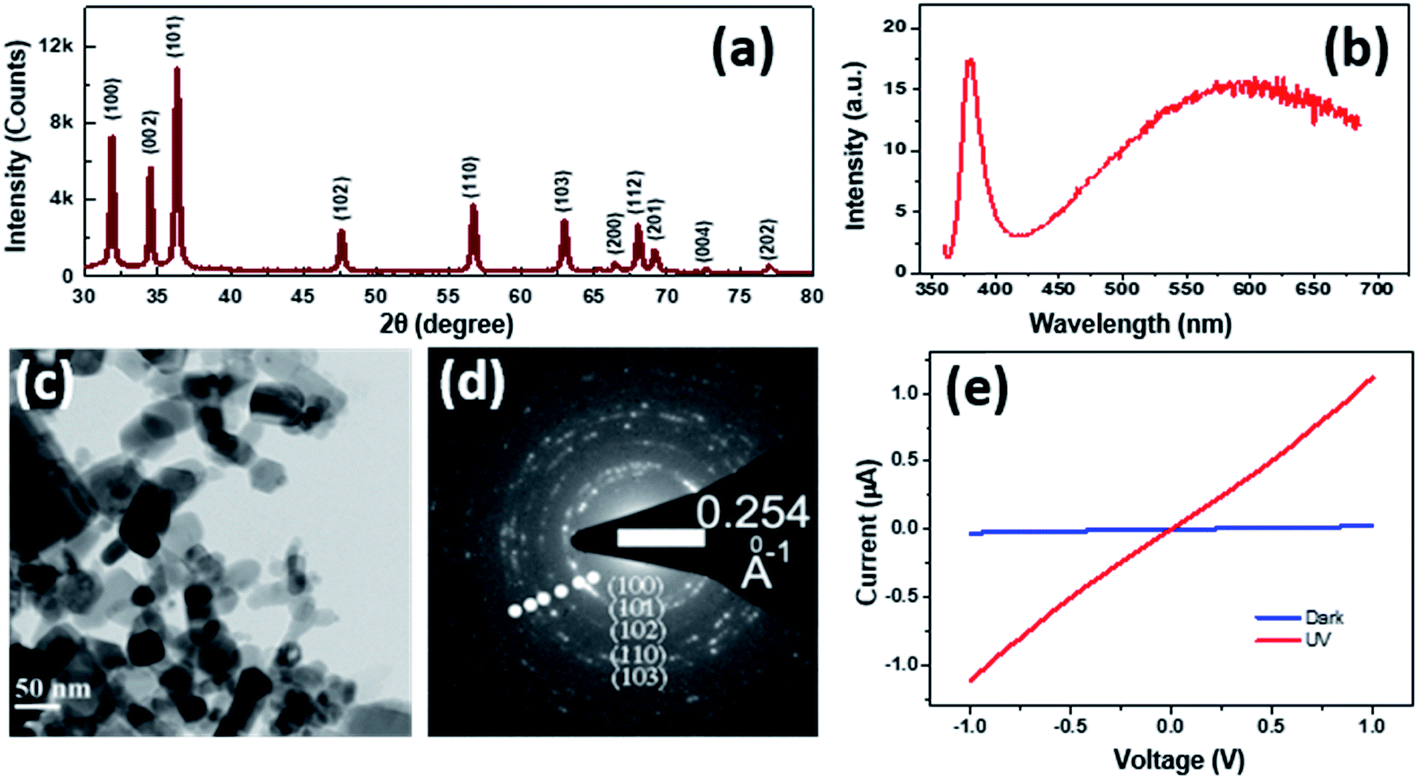
The powder XRD pattern (Fig. 1(a)) recorded on the as prepared ZNPs and peak indexing confirm the wurtzite structure of ZnO, evidencing the various crystal facets. The (101) peak shows the highest intensity followed by those from (100) and (002) planes. The TEM micrograph in Fig. 1(c) evidences an average ZNP dimension of ∼50 nm and the intense dots in the SAED pattern in Fig. 1(d) are indicative of the crystallinity of the ZNPs. Fig. 1(b) shows a typical photoluminescence spectrum from the nanocrystals, under 355 nm laser illumination. The sharp peak around 380 nm and the broad profile centred at 580 nm correspond to the near band edge and oxygen vacancy related emissions, as reported earlier.28Fig. 1(e) shows the IV characteristics of an assembly of ZNPs drop cast between 2 gold electrodes (100 microns apart). While the dark IV shows negligible conductance, that recorded under 355 nm illumination shows substantial increase in conductivity, with the zero bias conductance (dI/dV) increasing from 2.42 × 10⁻⁸ S in the dark to 1.06 × 10⁻⁶ S under illumination, conforming to the expected positive PR in ZnO. Prior to discussing the PR of the NC it’s worth benchmarking the morphology and energetics of the NC vis-à-vis those of its constituents. Fig. S1 (ESI†) shows the SEM image of the 50% NC film along with EDS elemental mapping for sulphur, zinc and silicon corresponding to their Kα emission. The bright regions in the SEM image show the clusters of ZNPs, which correlate with the brighter regions in the Zn Kα map and the darker regions of Si Kα. The S Kα map is expectedly devoid of contrast, originating homogeneously from the polymer matrix. Earlier reports of Raman spectroscopy on similar NCs have shown distinct changes to the Raman spectrum of PEDOT:PSS upon incorporation of ZNPs.23 Fig. S2(a) in the ESI† shows the Raman spectra of the bare polymer and the 50% NC. Apart from the various PEDOT:PSS related modes, the 50% NC also shows the 2LO mode of the ZNPs at 1128 cm−1. Importantly, the peak around 1440 cm−1, corresponding to the symmetric Cα = Cβ(−O) stretching mode of PEDOT:PSS, shows distinct differences when recorded on bare PEDOT:PSS and on the NC, as shown in Fig. S2(b) (ESI†). In bare PEDOT:PSS, de-convolution of this peak results in two peaks at 1435 cm−1 and 1453 cm−1, which have been attributed to the quinoid and benzoid structure of the PEDOT thiophene ring, respectively. In the NC, the higher wavenumber mode is not resolved i.e. the benzoid peak is quenched, which has been interpreted to indicate a more stretched (linear) configuration of the PEDOT chain,23 thereby increasing the ease of hole transport across the PEDOT chain and thus the conductivity of the NC compared to that of bare PEDOT:PSS. Further theoretical calculations show29 that the thiophene ring undergoes a benzoid to quinoid transformation when PEDOT0 is doped to PEDOT+ by removal of π conjugated electrons thus nucleating the hole carrier in PEDOT:PSS. A decrease in the abundance of the benzoid state (PEDOT0) with respect to the quinoid (PEDOT+) would thus aid electrical transport.
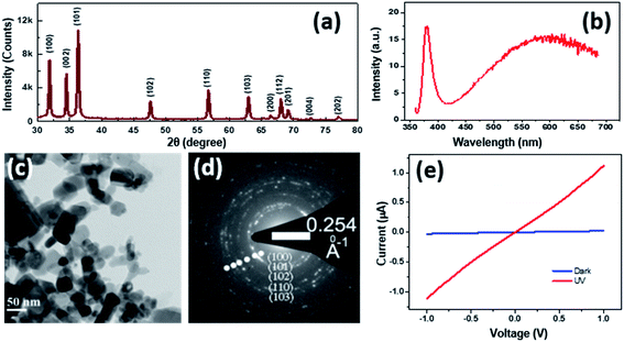 |
| | Fig. 1 Structural, luminescence and photoconducting properties of ZnO nanoparticles. (a) XRD pattern, (b) photoluminescence spectrum with 355 nm excitation, (c) TEM micrograph, (d) selected area electron diffraction, the assigned planes (white dots) read the planes away from the center and (e) IV characteristics of ZnO nanoparticles in the dark and with 355 nm UV excitation. | |
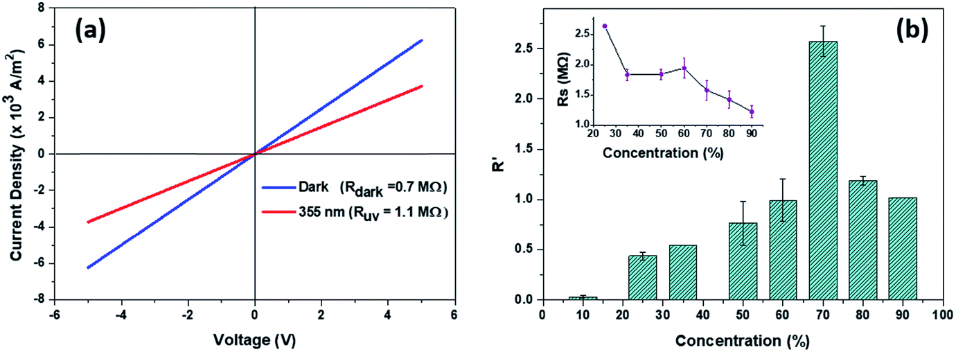
Fig. 2(a) shows the IV characteristics for a ZNP 50 wt% NC device in the dark and under UV illumination, between ±5 V. The linear IV curves indicate non-rectifying behaviour with a fractional resistance (R′ = (Rhν − Rdark)/Rdark) increase of 0.6 under UV illumination. R′ values for various concentrations of ZNPs in the polymer are obtained from the corresponding IV characteristics. Fig. 2(b) shows the variation of average R′ with ZNP wt%, varying between 10 and 90% for multiple measurements across 5 samples. The plot shows that the negative PR increases monotonically with ZNP concentration, reaching a maximum of 250% for 70 wt%. At higher ZNP wt%, R′ decreases rapidly, finally exhibiting positive PR for a pure ZNP system, as shown in Fig. 1(d). The inset of Fig. 2(b) shows the variation of dark resistance of the NC films for various concentrations of ZNPs. The positive PR of ZnO, especially in its nanostructured form with a large surface to volume ratio, is understood to originate from two sources, first, photogeneration of electrons excited across its band gap,10,11 which also affects the PR of n-ZnO based pn heterojunctions i.e. with PEDOT:PSS10 or p–Si30 and Schottky junctions with Au or Pt31etc. Second, the release of trapped free electrons from the surface adsorbed O2 molecules, via interaction with photogenerated holes, is also understood to increase the conduction band electron density.32,33 These freed electrons along with their photogenerated counterparts then contribute to the increase in conductance upon super band-gap (UV) illumination. It's relevant to note that the presence of the second mechanism significantly alters the overall temporal response of ZnO's photoconductivity,34,35 where the typical response time ranges from a few ms to tens of seconds or more. Time resolved photoexcitation experiments conducted in the absence of O2 show long response times, ∼tens of ms, whereas the presence of O2 (or indeed other oxidizing species) greatly reduces the response time to values between a few ms to seconds.32,33,36 Interestingly, the associated kinetics of these conduction electrons, strongly influenced by the oxygen vacancies in ZnO and surface adsorbed O2, leads to the observance of resistive switching in ZnO–PEDOT:PSS nanoscale heterojunctions.12
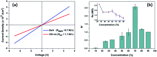 |
| | Fig. 2 (a) IV characteristics under dark conditions and UV illumination of the device with ZNP-50 wt%. (b) Histogram showing the variation of fractional PR [R′ = (Rhν − Rdark)/Rdark] with the concentration of ZnO nanoparticles. Error bars indicate the variation in measurements across 5 samples. The inset shows the sheet resistance in the dark of the NC with different ZNP concentrations. | |
Fig. 3(a) shows the plot of the time response of NC device resistance (scaled as R′) for various wt% of ZNPs under 355 nm excitation. The response curves were obtained by measuring the change in device resistance for a constant bias voltage of 5 V. Turning on UV illumination led to saturation at a higher resistance, which subsequently recovered to the original state once excitation was turned off. Analysis of the response time, following that discussed in ref. 11, yields a rise time constant (τr) and two distinct fast and slow decay time scales τd1 and τd2. The time constants vary with the wt% of ZNPs, though τr and τd1 are approximately an order of magnitude smaller than τd2. The inset of Fig. 3(a) shows the plot of the variation of τd2 with ZNP wt%. It increases from around 15 min at low concentrations to 30 min for 35% and then decreases to around 5 min for ZNP wt% > 50%. Fig. S3 (ESI†) shows the time response of one 50% sample for multiple UV illumination on–off cycles indicating the repeatability of the negative PR. Such large time constants likely arise due to the presence of trap states at the ZNP surface which presents a unique platform for optical control and storage. Fig. 3(b) shows the plot of the variation of average R′ with UV laser power measured across three 50% ZNP NC samples, indicating that the response saturates above 1 mW. The half-filled green circles correspond to spectrally resolved PR (top axis) of a 50% NC film when excited with a bare Xe lamp, having a significant UV component, and subsequently filtered through various long pass filters, with the cut-in wavelengths as indicated (in nm) in the top axis. It shows that even visible light excitation elicits negative PR from these samples though much subdued compared to that in the presence of UV. Yoo et al.21 have reported similar negative PR from ZnO–PEDOT:PSS NC nanowires under UV with comparable τd2. However the PR of the nanowires turned positive under visible light excitation, contrary to the present observations. Positive PR under UV and visible light excitation has been reported earlier by the authors for macroscale heterojunctions of ZnO–PEDOT:PSS10 and on the nanoscale for ZnO–Pt11,12 though the negative PR reported here is only observed for the nanocomposite configuration presented here.
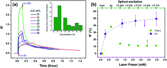 |
| | Fig. 3 (a) Temporal response of the different samples to UV illumination. The inset shows the variation of the decay time constant with ZNP wt%. (b) Device (50% NC) PR plotted for various intensities of UV illumination (bottom axis) and spectral response at various wavelengths (top axis). | |
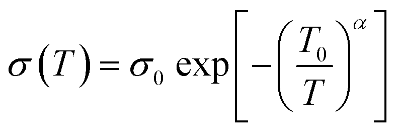
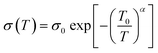
Electrical transport in hole doped organic systems like PEDOT:PSS is generally understood within the framework of variable range hopping (VRH).37–39 In the present case, temperature variation of resistance (ESI Fig. S5†) of a bare PEDOT:PSS thin film follows the 3 dimensional VRH model given by,
| |  | (1) |
where
σ is the film conductivity,
σ0 is the conductivity at infinite temperature,
T0 is a characteristic temperature and
α = 1/(1 +
D), with
D being the dimensionality of the system. The best-fit values of
σ0 and
T0 are 5 × 10
3 S cm
−1 and 6.4 × 10
6 K, respectively, with
D = 3, which are comparable with the reported values.
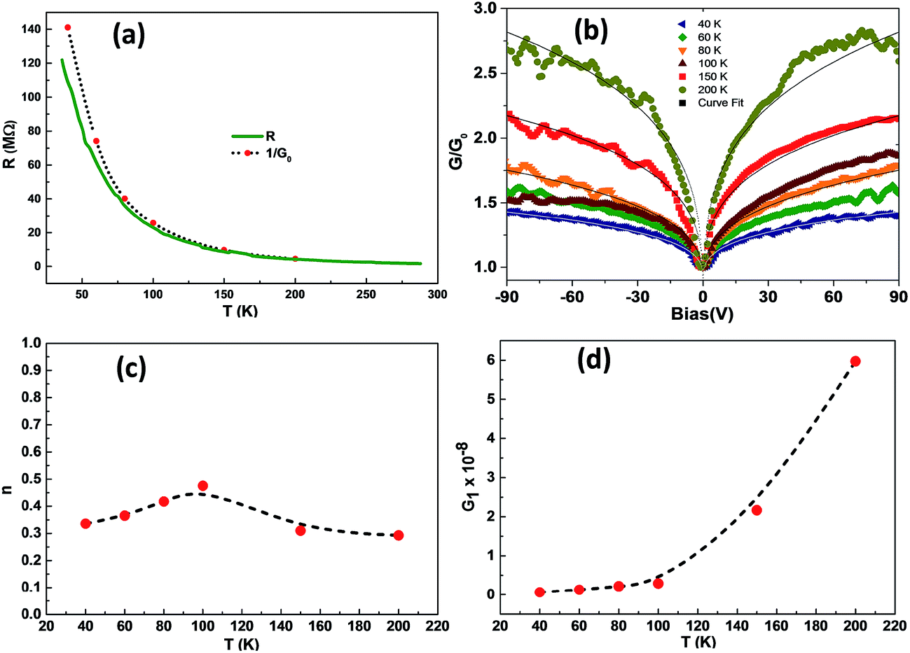
40Fig. 4(a) shows the measured resistance
vs. temperature data for the 50% NC film device depicting generic insulating behaviour (d
R/d
T < 0). Fit to
eqn (1) yields modified
σ0 = 0.2 × 10
3 S cm
−1 and
T0 = 3.6 × 10
6 K around 300 K, indicating that the VRH model adequately describes electrical transport in the ZnO/PEDOT:PSS NC around room temperature. In order to further comprehend the nature of electrical transport in the NC films, temperature dependent
IV characteristics, between ±100 V, were recorded as a function of temperature for the 50% thin film device. Though the low bias
IV data (shown in
Fig. 2(a)) indicate linear transport, it is non-linear at higher biases, with the systemic non-linearity accentuated in the observed temperature dependence.
Fig. 4(b) shows the normalized dynamic conductance (
G/
G0) data obtained by numerical differentiation of the
IV data at specific temperatures, where
G0 is the zero-bias conductance. Bias dependence of
G/
G0 data indicates symmetric, non-linear transport at all temperatures, interestingly, with the non-linearity decreasing with decreasing temperature. Temperature variation of the parameter 1/
G0, scatter plotted in
Fig. 4(a), follows that of the directly measured temperature dependence of the NC resistance. The nonlinearity in the conductance spectra is quantified by fitting the
G vs. V data to an empirical formula
41 of the form,
where
G0,
G1 and
n are temperature dependent parameters, the latter two quantifying the measure of non-linear transport. Temperature dependence of the three parameters, obtained by fitting the conductance data, is plotted in
Fig. 4(a), (c) and (d). While
G0 and
G1 show a significant decrease with decreasing temperature,
n (∼0.4) appears to be weakly dependent on temperature. Comprehending the observed decrease in nonlinearity (
G1) with decreasing temperature is non-trivial though the value of the exponent
n < 1 alludes to carrier localisation effects on electrical transport across the NC film. The typical localization energy (Δ
E) estimated from the parameters
G0,
G1 and
n gave Δ
E ∼ 1.07 eV above 200 K.
 |
| | Fig. 4 (a) Comparison of the resistance R of the ZNP-50 wt% device and 1/G0 as a function of temperature. (b) Normalized dynamic conductance G/G0 as a function of applied bias voltage at different temperatures. Solid lines indicate fits to eqn (2). Temperature dependence of fit parameters (c) n and (d) G1. | |
In the dark, conduction in the NC samples occurs dominantly through the PEDOT:PSS background since the dispersed ZNPs have significantly lower conductivity, which changes dramatically upon UV illumination. The observed increase in resistance (negative PR) upon UV illumination cannot be attributed to resistance change due to illumination induced heating of either PEDOT:PSS37 or ZnO as both systems exhibit a negative temperature coefficient of resistance. Neither can it be attributed to the PR of PEDOT:PSS, which has negligible absorption and PR between 300 and 800 nm (see the supplementary information of ref. 10), leading us to conclude that the negative PR effect originates from that of ZNPs. PEDOT:PSS is a complex formed by PEDOT grains embedded in the PSS matrix.42 The p-type doping of PEDOT:PSS i.e. the PEDOT+ state is stabilised by the presence of the sulfonate group in PSS,43 which also makes the complex water soluble. Fig. S3(b) shows a schematic of PEDOT+:PSS, indicating the presence of a hole that transports along the PEDOT backbone guided by the applied electric field. The presence of PSS around the PEDOT grains further inhibits charge transport between the PEDOT grains, which likely happens by the interplay of the tunnelling and percolating PEDOT network. Overall it results in a VRH type transport across the polymer as discussed earlier.40 Any mechanism that results in localization of carriers (holes) in PEDOT:PSS would thus increase its resistance. Bare ZnO's n-type conductivity (free electron density) originates from intrinsic defect donors and perhaps incorporated hydrogen.28,44,45 These electrons are understood to form complexes with the electronegative atmospheric oxygen molecules – that are adsorbed onto the surface. In the NC, each ZNP embedded in the PEDOT:PSS matrix forms an extended Schottky junction along its surface, with a barrier height of 0.8 eV.46 Since the polymer completely encapsulates individual ZNPs, so does the interfacial barrier. It's worth noting that in measuring the electrical properties of the NC device, a bias is applied to the polymer matrix and the voltage drops primarily along the polymer conduction channel and not explicitly across the Schottky junctions formed at the individual ZNP surfaces47 – in contrast to the case of standard planar heterojunction devices. Further any bias (either positive or negative) applied across the NC film results in negligible i.e. practically zero, voltage drop at the dimension of individual ZNPs (50 nm). Thus the application of device bias, and subsequent ramping, does not dynamically induce band bending in ZNPs either close to or away from their surface, again in contrast to the case of planar junction devices.10 Consequently this collection of encapsulated Schottky junctions displays non-rectifying, symmetric IV characteristics (Fig. 4(b)) that are dominantly linear up to ±5 V bias (Fig. 2(a)). In the absence of any explicit bias appearing across the junction free electrons in ZNPs are trapped via the barrier. The free electrons at the surface of ZNPs would still interact with the holes or their associated electronegative charge centres in PEDOT:PSS, establishing an equilibrium, a Fermi level alignment across the interface. Thus even in the dark the conductivity of the NC i.e. ZNP incorporated PEDOT:PSS should be lower than that of bare PEDOT:PSS. This is corroborated by the decrease in the value of σ0 (eqn (1)) corresponding to the bare polymer and 50% NC. Earlier reports23,48 on similar NCs, however, have shown the opposite behaviour, i.e. increase in PEDOT:PSS conductivity with 10–20% ZNP incorporation. The effect has been attributed to improved transport in the NC due to linearization of the PEDOT:PSS chains – evidenced by the disappearance of the benzoid peak in the Raman spectra, as discussed earlier. Though we observe the reported change in the Raman spectra the conductivity of the film did not increase upon ZNP incorporation. The inset of Fig. 2(b) indicates a decreasing trend in NC resistance (in the dark) with increasing ZNP percentage, which needs to be probed more intensively for obtaining any conclusive inferences.
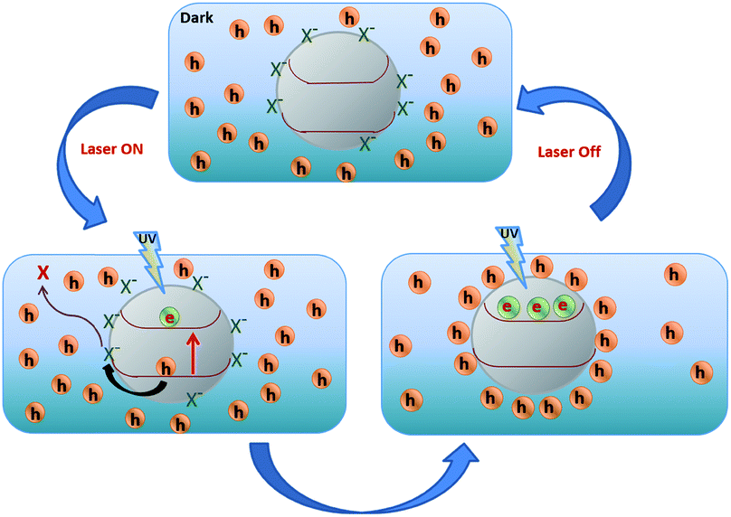
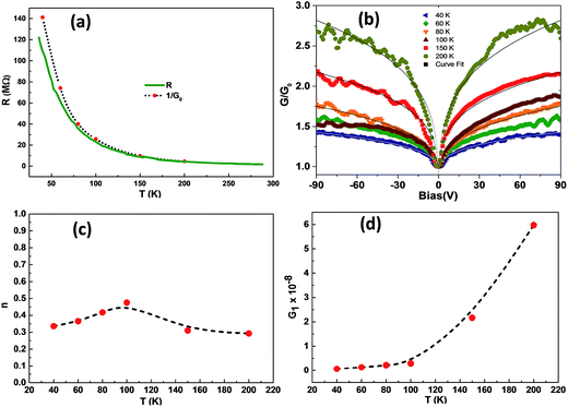
Fig. 5 shows a schematic of the interaction between the free electrons in ZNPs and X−, which denotes the electronegative centres or holes that passivate the surface electron density of ZNPs. Once the NC is illuminated with UV excitation free electrons are generated in the conduction band of ZnO, making the ZNPs electron rich, which remain trapped in the ZNPs due to the interfacial barrier, inducing strong interaction with the PEDOT holes with two distinct consequences. First, it creates an interfacial capacitive charge double layer along the ZNP surface accompanied by a strong interfacial electric field and a large junction capacitance (CJ). Second, localisation of holes in the polymer (Fig. 5) or local reduction of PEDOT+ increases the device resistance. The effect is similar to traditional voltage gating in electronic devices where an applied dc field changes the accumulated carrier density in an active channel. Here the photogenerated carriers trap the holes and inhibit transport in the polymer. Charge accumulation at the capacitive junction upon UV illumination is effectively a case of photo-gating of the PEDOT conduction pathway where the effective density of available holes is tuned by the UV illumination, evidenced via the negative PR (Fig. 3(a)) and its spectral dependence (Fig. 3(b)). The strong electric field induced at the ZNP surface inhibits carrier recombination therein with the large CJ and is reflected in the slow PR of the system, especially in the large decay time constant (τ = RJCJ, where RJ is the junction resistance) of several minutes. The effect arises due to the quasi-zero bias across any of the ZnO–PEDOT:PSS interfaces, eliminating any significant charge transport across the junction. The absence of explicit bias across the junction also precludes investigation of bias dependence of the time constants and thus CJ. However, planar junctions of n-ZnO–PEDOT:PSS show a distinct bias dependence of positive PR τdecay, as shown in Fig. S6 (ESI†). τdecay shows an appreciable increase with decreasing reverse bias current (−50, −40 and −30 μA) with τdecay = 31 s, 47 s and 120 s corresponding to CJ = 0.5 μF, 0.8 μF and 2.3 μF (calculated using dynamic RJ of the dark IV), respectively. Constant current mode detection of PR allows us to directly monitor variation in accumulated charge (QJ) with junction potential (VJ) following QJ = CJVJ.11 Note that even for the planar junctions the decay time constants are in minutes which are longer than that of bare ZnO, and the trend of increasing CJ with decreasing reverse bias extrapolates to still longer τ at zero bias, which is the case in the NC investigated here.
 |
| | Fig. 5 Schematic of the negative PR mechanism under on–off UV excitation (X− is an electronegative species e.g. adsorbed oxygen). | |
Energy level comparison of the HOMO LUMO states of the polymer and conduction and valence bands of ZnO vis-à-vis PEDOT:PSS indicates that electron injection from ZnO into the LUMO states of the polymer i.e. reduction of PEDOT+ to PEDOT0 increases the band gap of the polymer. It's worth noting that permanent neutralization of the hole space charge in PEDOT:PSS for planar junctions with Au and ITO, by injection of electrons into PEDOT, above critical junction biases (∼2 V) has been reported before49 with clear signatures in the IV characteristics. The zero junction bias in the present case and the time response data shown in Fig. 3(a) and S3 (ESI†), evidencing the reversible nature of the negative PR, indicate that photoexcitation does not result in photocatalytic degradation of the polymer due to the photoactivity of ZNPs. This also reinforces the assumed absence of photogenerated electron ejection from ZNPs out to the polymer, as discussed above. The negative PR effect is expected to be a function of ZNP loading in PEDOT:PSS since it would be a function of the overall ZNP surface area i.e. effective area of the junctions, thus it increases with an increase in the percentage of ZNPs, as shown in Fig. 2(b). The physical understanding presented above tacitly assumes that the ZNPs are well dispersed in the polymer and there are no percolating agglomerates of ZNPs across the NC, which might form a transport pathway between the source and drain electrodes in parallel to that through the polymer. Above a critical loading of ZNPs this assumption would break down. Once large continuous domains of ZNPs form, a significant fraction of the applied bias will drop along the domains allowing transport through them thus reducing the fractional resistance change of the NC device. Experimentally this was evidenced by a drop in R′ for ZNP wt% > 70% (Fig. 2(b)). A final confirmation of the negative PR of the NC was obtained from spatially resolved photocurrent maps. Fig. 6 shows four sets of AFM topography images and the corresponding current maps of a 50% NC film, acquired sequentially in the dark and with 0.5 h and 3 h of UV illumination and finally again in the dark i.e. after UV illumination was turned off, at 3.5 h. The current map recorded in the dark shows contrast likely arising out of topographical features (see blue arrow) with a large average current of 10 nA. Upon UV illumination the current map becomes devoid of contrast and the average current decreases to 165 pA and 16 pA after 0.5 h and 3 h of continued illumination. The corresponding topography retains the topographic features although with a finite drift in the investigated area (blue arrows indicate progressive drift of the elliptical feature to the left of the image). It is worth noting that the simultaneously conducted dI/dV mapping of the NC film surface, under UV illumination, also evidenced a homogeneous decrease in surface conductance indicating that as prepared the present samples do not allow spatial discrimination of charge localisation via the electrical scanning probe techniques employed. We are in the process of tailoring suitable samples with n-type nanoparticles in a p-type matrix with strong photogating effects that may provide sufficient resolution to discriminate between charges that are migrated to/from the surface due to embedded nanoparticles and those localised around the nanoparticles at the surface, under UV illumination.
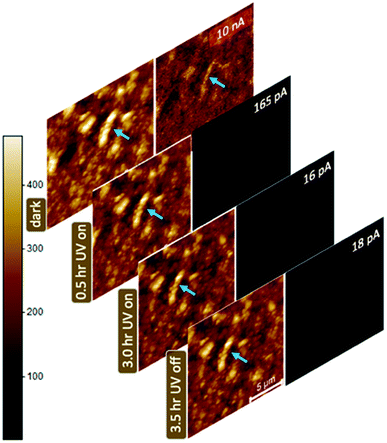 |
| | Fig. 6 Series of AFM topography and current maps acquired on a 50% NC sample in the dark and at different durations of UV illumination and after UV was turned off, as indicated. The lateral scale bar is 5 μm, and the topographic z range is shown in the colour bar in nm. The current map colour range is 120 nA and was recorded under 2 V sample bias. The average current is recorded in each current map. | |
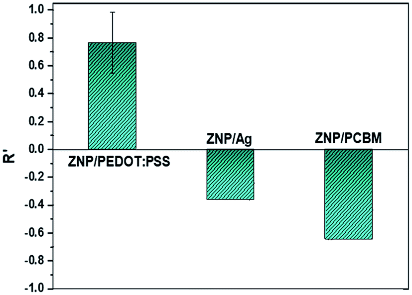
Finally, to test the hypothesis that the negative PR arises out of an effective decrease in mobile holes in PEDOT:PSS due to photogenerated electrons trapped in the ZNPs and elucidate the role of the surface barrier vis-à-vis the n and p type nature of the ZNPs and the polymer, the above experiments were repeated with NCs of ZNPs in materials that transport electrons rather than holes. Ag paste and a C60 fullerene based n-type organic semiconductor (PCBM) were chosen as the electron transport materials for various reasons. First, the energy difference between the Fermi level of Ag and the conduction band minimum of ZnO is less than 100 meV indicating that the Schottky barrier height of the ZNP–Ag nanocomposite will be small such that electrons will be effectively transported out across the interfacial barrier. Second, the PCBM–ZnO interface is well researched in the domain of solar cells where ZnO is routinely used as an electron-extracting layer. The PRs of both these NCs for ZNP-50 wt% devices are shown in Fig. 7, exhibiting the expected positive PR under UV illumination, as photogenerated electrons in ZnO increase the ZNP carrier density decreasing the overall resistance of the devices.
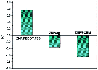 |
| | Fig. 7 Histogram showing device response for a ZNP-50 wt% device of ZNPs in Ag paint and ZNPs in PCBM. In comparison to the negative PR in the ZNP/PEDOT:PSS NC, ZNP/Ag and ZNP/PCBM show positive PR under UV (355 nm) illumination. | |
Conclusion
The optoelectronics of nanocomposites of inorganic semiconductors in a p-type organic polymer show various performance improvements compared to those of their planar counterparts – exhibiting novel effects not observed otherwise. Here we have investigated one such effect, negative PR (increase in resistance) upon UV illumination in nanocomposites of ZnO nanoparticles in PEDOT:PSS. The nanocomposite comprises nanoscale junctions of ZnO and PEDOT:PSS dispersed uniformly across the fabricated thin films. The results indicate that the negative PR increases with wt% of ZNPs in PEDOT:PSS and arises due to charge interaction at the junctions. Photogenerated electrons in the ZnO nanoparticles, trapped at the junction due to the surface barrier, localise the carriers (holes) in the primary conduction channel (PEDOT), thus decreasing the net carrier density and increasing the overall resistance. The absence of any net bias across the interfacial junction is understood to be central to negative PR and the large response times, originating from the charge double layer trapped at the nanoparticle surface inducing a large junction capacitance. The negative PR persists until a critical loading of nanoparticles beyond which the device PR starts decreasing with the formation of extended nanoparticle agglomerates. Temperature dependent transport studies and temporal response showing large decay timescales provide further information regarding the optoelectronic properties and charge transport in these nanocomposites especially in the presence of dispersed nanoscale junctions. From a fundamental perspective, this investigation provides new insights into transport in heterogeneous nanostructured media in which photoexcitation induced carrier trapping and localisation offers a versatile control parameter. Applications of photogating to energy harvesting and optical signal manipulation are envisaged.
Conflicts of interest
There are no conflicts to declare.
Acknowledgements
J. M. acknowledges financial support from the University Grants Commission and Department of Science and Technology, Government of India; UKIERI; the Royal Academy of Engineering; and the Newton Bhabha Fund, UK. H. G. acknowledges the DST for an INSPIRE fellowship. K. N. P. acknowledges a studentship from the IISER, Thiruvananthapuram.
References
- Y. Jin,
et al., Solution-processed ultraviolet photodetectors based on colloidal ZnO nanoparticles, Nano Lett., 2008, 8(6), 1649–1653 CrossRef CAS PubMed.
- Y. Li,
et al., High-performance UV detector made of ultra-long ZnO bridging nanowires, Nanotechnology, 2008, 20(4), 045501 CrossRef PubMed.
- Y. Han,
et al., Highly efficient ultraviolet photodetectors based on TiO2 nanocrystal–polymer composites via wet processing, Nanotechnology, 2010, 21, 185708 CrossRef PubMed.
- H. Xue,
et al., TiO2 based metal-semiconductor–metal ultraviolet photodetectors, Appl. Phys. Lett., 2007, 90(20), 201118 CrossRef.
- H. Kim,
et al., Effect of film thickness on the properties of indium tin oxide thin films, J. Appl. Phys., 2000, 88(10), 6021–6025 CrossRef CAS.
- C. G. Granqvist and A. Hultåker, Transparent and conducting ITO films: new developments and applications, Thin Solid Films, 2002, 411(1), 1–5 CrossRef CAS.
- H. M. Kim, T. W. Kang and K. S. Chung, Nanoscale Ultraviolet-Light-Emitting Diodes Using Wide-Bandgap Gallium Nitride Nanorods, Adv. Mater., 2003, 15(7–8), 567–569 CrossRef CAS.
- V. A. Fonoberov and A. A. Balandin, Origin of ultraviolet photoluminescence in ZnO quantum dots: Confined excitons versus surface-bound impurity exciton complexes, Appl. Phys. Lett., 2004, 85(24), 5971 CrossRef CAS.
- I. Shalish, H. Temkin and V. Narayanamurti, Size-dependent surface luminescence in ZnO nanowires, Phys. Rev. B: Condens. Matter Mater. Phys., 2004, 69, 245401 CrossRef.
- S. Vempati,
et al., Unusual photoresponse of indium doped ZnO/organic thin film heterojunction, Appl. Phys. Lett., 2012, 100(16), 162104 CrossRef.
- K. Bandopadhyay and J. Mitra, Spatially resolved photoresponse on individual ZnO nanorods: correlating morphology, defects and conductivity, Sci. Rep., 2016, 6, 28468 CrossRef CAS PubMed.
- K. Bandopadhyay, K. N. Prajapati and J. Mitra, Resistive switching in individual ZnO nanorods: delineating the ionic current by photo-stimulation, Nanotechnology, 2018, 29, 105701 CrossRef CAS PubMed.
- O. F. Yilmaz, S. Chaudhary and M. Ozkan, A hybrid organic–inorganic electrode for enhanced charge injection or collection in organic optoelectronic devices, Nanotechnology, 2006, 17, 3662–3667 CrossRef CAS.
- Y. Tu,
et al., Transparent and flexible thin films of ZnO-polystyrene nanocomposite for UV-shielding applications, J. Mater. Chem., 2010, 20(8), 1594–1599 RSC.
- P. P. Jeeju and S. Jayalekshmi, On the Interesting Optical Properties of Highly Transparent, Thermally Stable, Spin-Coated Polystyrene/Zinc Oxide Nanocomposite Films, J. Appl. Polym. Sci., 2011, 120(3), 1361–1366 CrossRef CAS.
- A. Somwangthanaroj,
et al., Effect of zinc precursor on thermal and light emission properties of ZnO nanoparticles embedded in polyimide films, Mater. Chem. Phys., 2009, 114(2–3), 751–755 CrossRef CAS.
- H.-M. Xiong,
et al., Stable Aqueous ZnO@Polymer Core–Shell Nanoparticles with Tunable Photoluminescence and Their Application in Cell Imaging, J. Am. Chem. Soc., 2008, 130, 7522–7523 CrossRef CAS PubMed.
- L. Zhang,
et al., Stably dispersible P3HT/ZnO nanocomposites with tunable luminescence by in situ hydrolysis and copolymerization of zinc methacrylate, J. Lumin., 2010, 130(12), 2332–2338 CrossRef CAS.
- S. R. Forrest, The path to ubiquitous and low-cost organic electronic appliances on plastic, Nature, 2004, 428, 911–918 CrossRef CAS PubMed.
- H. M. Thirimanne,
et al., High sensitivity organic inorganic hybrid X-ray detectors with direct transduction and broadband response, Nat. Commun., 2018, 9(1), 2926 CrossRef CAS PubMed.
- J. Yoo, J. Pyo and J. H. Je, Single inorganic–organic hybrid nanowires with ambipolar photoresponse, Nanoscale, 2014, 6(7), 3557–3560 RSC.
-
A. Elschner, et al., PEDOT: principles and applications of an intrinsically conductive polymer, CRC Press, 2010 Search PubMed.
- N. G. Semaltianos,
et al., Modification of the electrical properties of PEDOT:PSS by the incorporation of ZnO nanoparticles synthesized by laser ablation, Chem. Phys. Lett., 2010, 484(4–6), 283–289 CrossRef CAS.
- A. A. Tursun Abdiryim, R. Jamal, Y. Osman and Y. Zhang, A facile solid-state heating method for preparation of poly(3,4-ethelenedioxythiophene)/ZnO nanocomposite and photocatalytic activity, Nanoscale Res. Lett., 2014, 9, 89 CrossRef PubMed.
- C. Leow,
et al., Light-soaking effects on ZnO-nanorods/polymer hybrid photovoltaics, RSC Adv., 2015, 5(29), 22647–22653 RSC.
- N. Gupta,
et al., A simple technique for the fabrication of zinc oxide-PEDOT:PSS nanocomposite thin film for OLED application, Synth. Met., 2016, 221, 261–267 CrossRef CAS.
- P. Uthirakumar, H. G. Kim and C.-H. Hong, Zinc oxide nanostructures derived from a simple solution method for solar cells and LEDs, Chem. Eng. J., 2009, 155(3), 910–915 CrossRef CAS.
- K. Bandopadhyay and J. Mitra, Zn interstitials and O vacancies responsible for n-type ZnO: what do the emission spectra reveal?, RSC Adv., 2015, 5(30), 23540–23547 RSC.
- A. Lenz,
et al., The electronic structure and reflectivity of PEDOT:PSS from density functional theory, Chem. Phys., 2011, 384(1–3), 44–51 CrossRef CAS.
- S. Mridha and D. Basak, Ultraviolet and visible photoresponse properties of n-ZnO/p–Si heterojunction, J. Appl. Phys., 2007, 101(8), 083102 CrossRef.
- K. Ul Hasan,
et al., Single nanowire-based UV photodetectors for fast switching, Nanoscale Res. Lett., 2011, 6(1), 1–6 Search PubMed.
- S.-E. Ahn,
et al., Origin of the slow photoresponse in an individual sol–gel synthesized ZnO nanowire, Appl. Phys. Lett., 2007, 90(15), 153106 CrossRef.
- C. Soci,
et al., ZnO nanowire UV photodetectors with high internal gain, Nano Lett., 2007, 7(4), 1003–1009 CrossRef CAS PubMed.
- S. E. Ahn,
et al., Photoresponse of sol–gel-synthesized ZnO nanorods, Appl. Phys. Lett., 2004, 84(24), 5022–5024 CrossRef CAS.
- L. Xu,
et al., Catalyst-Free, Selective Growth of ZnO Nanowires on SiO2 by Chemical Vapor Deposition for Transfer-Free Fabrication of UV Photodetectors, ACS Appl. Mater. Interfaces, 2015, 7(36), 20264–20271 CrossRef CAS PubMed.
- Q. H. Li,
et al., Adsorption and desorption of oxygen probed from ZnO nanowire films by photocurrent measurements, Appl. Phys. Lett., 2005, 86(12), 123117 CrossRef.
- A. M. Nardes, R. A. J. Janssen and M. Kemerink, A Morphological Model for the Solvent-Enhanced Conductivity of PEDOT:PSS Thin Films, Adv. Funct. Mater., 2008, 18(6), 865–871 CrossRef CAS.
- M. Pollak and I. Riess, A percolation treatment of high-field hopping transport, J. Phys. C: Solid State Phys., 1976, 9(12), 2339 CrossRef.
- L. I. Glazman and K. A. Matveev, Inelastic tunneling across thin amorphous films, JETP Lett., 1988, 67(6), 1276 Search PubMed.
- A. M. Nardes, M. Kemerink and R. A. J. Janssen, Anisotropic hopping conduction in spin-coated PEDOT:PSS thin films, Phys. Rev. B: Condens. Matter Mater. Phys., 2007, 76(8), 085208 CrossRef.
- L. Peñate-Quesada, J. Mitra and P. Dawson, Non-linear electronic transport in Pt nanowires deposited by focused ion beam, Nanotechnology, 2007, 18(21), 215203 CrossRef.
- M. M. de Kok,
et al., Modification of PEDOT:PSS as hole injection layer in polymer LEDs, Phys. Status Solidi A, 2004, 201(6), 1342–1359 CrossRef CAS.
- L. Groenendaal,
et al., Poly(3,4-ethylenedioxythiophene) and Its Derivatives: Past, Present, and Future, Adv. Mater., 2000, 12(7), 481–494 CrossRef CAS.
- W.-W. Feng,
et al., Co-contribution of hydrogen impurities and native defects might be the answer for the n-type conductivity in ZnO, Phys. Lett. A, 2016, 380(3), 480–484 CrossRef CAS.
- A. Janotti and C. G. Van de Walle, Native point defects in ZnO, Phys. Rev. B: Condens. Matter Mater. Phys., 2007, 76(16), 165202 CrossRef.
- T. Nagata,
et al., Hard X-ray photoelectron spectroscopy study on band alignment at poly(3,4-ethylenedioxythiophene):poly(styrenesulfonate)/ZnO interface, Appl. Phys. Lett., 2012, 101(17), 173303 CrossRef.
- J. Mitra,
et al., An alternative methodology in Schottky diode physics, J. Appl. Phys., 2015, 117(24), 244501 CrossRef.
- Y.-J. Lin,
et al., Carrier transport mechanism of poly(3,4-ethylenedioxythiophene) doped with poly(4-styrenesulfonate) films by incorporating ZnO nanoparticles, Appl. Phys. Lett., 2012, 100(25), 129 Search PubMed.
- S. Moller,
et al., A polymer/semiconductor write-once read-many-times
memory, Nature, 2003, 426, 166 CrossRef PubMed.
Footnotes |
| † Electronic supplementary information (ESI) available. See DOI: 10.1039/c9na00116f |
| ‡ Currently in Jagiellonian University, Poland. |
| § Currently in the National University of Singapore, Singapore. |
|
| This journal is © The Royal Society of Chemistry 2019 |
Click here to see how this site uses Cookies. View our privacy policy here. 
 Open Access Article
 This Open Access Article is licensed under a Creative Commons Attribution-Non Commercial 3.0 Unported Licence
 *a,
Sesha
Vempati
b,
K. N.
Prajapati
a,
K.
Bandopadhyay‡
*a,
Sesha
Vempati
b,
K. N.
Prajapati
a,
K.
Bandopadhyay‡