
 Open Access Article
 This Open Access Article is licensed under a Creative Commons Attribution-Non Commercial 3.0 Unported Licence
Epitaxial patterned Bi2FeCrO6 nanoisland arrays with room temperature multiferroic properties†
Wei
Huang‡
 a,
Shun
Li‡
bc,
Soraya
Bouzidi
d,
Lei
Lei
e,
Zuotai
Zhang
c,
Ping
Xu
e,
Sylvain G.
Cloutier
d,
Federico
Rosei
*a and
Riad
Nechache
*d
a,
Shun
Li‡
bc,
Soraya
Bouzidi
d,
Lei
Lei
e,
Zuotai
Zhang
c,
Ping
Xu
e,
Sylvain G.
Cloutier
d,
Federico
Rosei
*a and
Riad
Nechache
*d
aINRS-Centre Énergie, Matériaux et Télécommunications, 1650, Boulevard Lionel-Boulet, Varennes, Québec J3X 1S2, Canada. E-mail: rosei@emt.inrs.ca
bSUSTech Academy for Advanced Interdisciplinary Studies, Southern University of Science and Technology, Shenzhen 518055, The People's Republic of China
cSchool of Environmental Science and Engineering, Southern University of Science and Technology, Shenzhen 518055, The People's Republic of China
dÉcole de Technologie Supérieure, 1100 Rue Notre-Dame Ouest, Montréal, Québec H3C 1K3, Canada. E-mail: Riad.Nechache2@etsmtl.ca
eCollege of Electronic Science and Technology, Shenzhen University, Nanhai Ave 3688, Shenzhen 518060, The People's Republic of China
First published on 13th May 2019
Abstract
Epitaxial multiferroic Bi2FeCrO6 nanoisland arrays with a lateral size of ∼100 nm have been successfully fabricated by patterned SiO2 template-assisted pulsed laser deposition. The as-grown island structure exhibits promising multiferroic properties (i.e. ferroelectric and magnetic) even at nanometer dimensions at room temperature. This work demonstrates an effective strategy to fabricate high-density nonvolatile ferroelectric/multiferroic memory devices.
Recently, ferroelectric materials have been considered promising as active systems for the development of multiple technologies.1,2 Due to their non-volatility and ultra-low energy consumption, such materials are currently being exploited for various applications such as memory devices, actuators and microelectromechanical systems.3,4 Although continuous ferroelectric thin films have been the focus of several studies in the past few decades, the increasing demand for high density data storage devices has motivated substantial efforts in fabricating ferroelectric nanostructures.5–8 Low-dimensional ferroelectric nanostructures such as nanoparticles, nanowires/tubes, nanosheets, and nanorings have been widely studied to improve their ferroelectric polarization promoted by confinement effects and the formation of single domain structures.9–14 In particular, highly ordered arrays of ferroelectric nanostructures are ideal candidates since the cross-talking between different ferroelectric cells in continuous films invoked by domain movements or thermal diffusion could be inherently excluded in such nanostructures.15–17 Until now, top-down nano-patterned arrays have been fabricated for several ferroelectric systems, such as PbTiO3,18,19 BaTiO3,20 and P(VDF-TrFE) polymers,15 showing reversal of ferroelectric polarization behavior down to a few nanometers and suggesting great potential for high-density non-volatile memory devices.
Multiferroic materials that combine two or more ferroic functionalities (e.g., ferroelectric, ferromagnetic and ferroelastic) are especially promising for applications such as spintronics, non-volatile data storage and optoelectronic devices.21–25 The magnetic–ferroelectric coupling in multiferroics can be used to encode information via electric polarization and magnetization, e.g., a four logic-state memory.26,27 Among all multiferroic materials, Bi-based perovskite oxides including BiFeO3 (BFO) and Bi2FeCrO6 (BFCO) exhibit large ferroelectricity and ferromagnetism and are therefore promising for practical applications.11,23 As one of the most important single-phase multiferroic perovskites, BFO thin films and nanostructures have been widely studied due to their superior ferroelectricity, unexpected domain wall functionalities, strong magnetoelectric coupling, etc.11,28–32 At the same time, the multiferroic double-perovskite BFCO thin films have emerged as an attractive system with outstanding physical properties for photovoltaic, spintronic and photocatalytic applications.23,33–37 While BFO nanostructures have been investigated extensively, very few reports have explored BFCO nanostructures. We previously reported the fabrication of sub-micrometer sized multiferroic BFCO patterns by pulsed laser deposition (PLD) via nanostencil lithography.38 To achieve ultra-high-density electronic devices, it is necessary to further reduce the BFCO structural dimensions to fabricate nanocapacitors and/or nanoisland arrays.
Here, we grew BFCO nanostructures by PLD using an ultra-thin SiO2 template patterned using e-beam lithography. Finally, the SiO2 mask is easily removed by immersion into alkaline solution to leave a highly ordered periodic array of free-standing BFCO nanoislands on an Nb-doped SrTiO3 (NSTO) (100) substrate. The typical dimensions of the BFCO nanoislands are around 100 nm in diameter with a height of about 120 nm. Most importantly, the resulting nanoarrays exhibit both ferroelectric and magnetic switching properties, illustrating the multifunctional properties of the BFCO structures at the nanoscale.
The fabrication process of the patterned SiO2 hard mask is schematically illustrated in Fig. 1 (Step I). Subsequently this pre-patterned SiO2 hard mask/NSTO is used for the direct deposition of BFCO to produce highly ordered periodic nanoisland arrays, such as those shown in Fig. 1 (Step II). In contrast, continuous thin films could be carved into discrete nanostructures by using a focused-ion beam (FIB). However, the crystal structure of these nanostructures could be affected and easily damaged during the etching process. Here, solution-based alkali removal of the SiO2 hard mask offers a promising alternative approach to obtain epitaxial-quality ferroelectric nanoisland structures.
 | ||
| Fig. 1 Schematic diagram of the process flow for the fabrication of BFCO nanoisland arrays. Fabrication of the patterned SiO2 hard mask (Step I): (1) deposition of SiO2 thin films by PECVD; (2) application of resist PMMA; (3) e-beam lithography; (4) development and resist removal; (5) dry etching of the SiO2 hard mask; (6) resist PMMA stripping. Fabrication of BFCO nanoisland arrays (Step II): (7) growth of BFCO nanoisland arrays on the NSTO substrate by PLD using the pre-patterned SiO2 template; (8) removal of the template to leave the nanopatterned arrays by immersing the substrate into a NaOH solution. | ||
Scanning electron microscopy (SEM) and atomic force microscopy (AFM) are used to characterize the morphology of the SiO2 hard mask on the NSTO substrate, as shown in Fig. 2. The SEM image (Fig. 2(a)) clearly shows periodic holes of ∼100 nm diameter with a spacing width of ∼1.0 µm. Precise pattern transfer from PMMA to SiO2 is achieved using a well-controlled plasma etching process with only a slight size increase of less than 5%. In addition, good pore size uniformity is maintained, with a standard deviation of less than 5% across a 70 × 70 µm2 area. Moreover, the high-resolution topography of the SiO2 hard mask is further examined by AFM (Fig. 2(b)). According to the line scan profile (Fig. 2(c)), the holes are ∼100 nm in diameter and ∼150 nm in depth after etching.
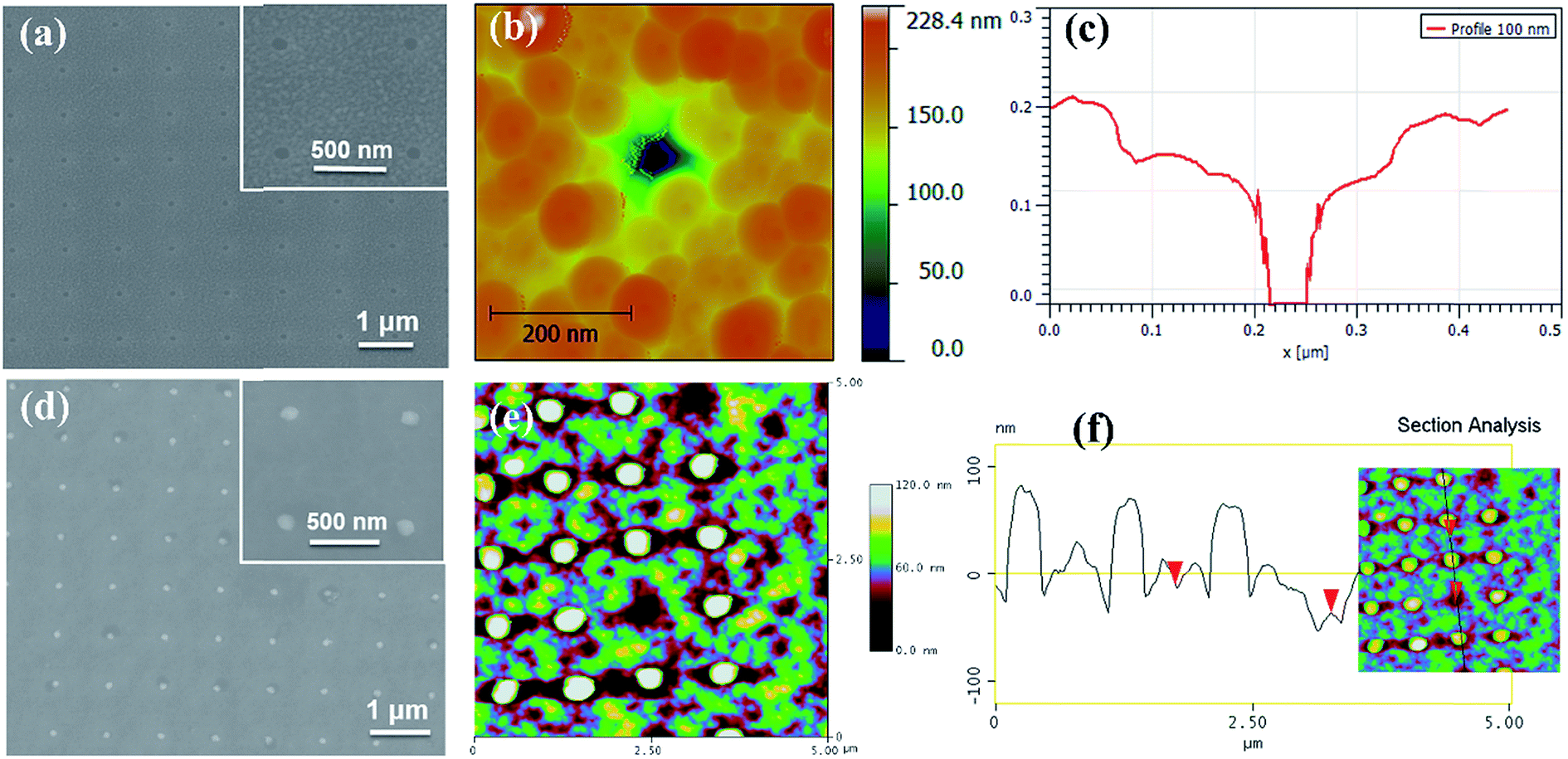 | ||
| Fig. 2 (a) SEM micrograph (inset shows the magnified view), (b) AFM topography image, and (c) depth profile of the SiO2 hard mask. (d) SEM micrograph (inset shows the magnified view), (e) AFM topography image, and (f) depth profile of the BFCO nanoisland arrays after removing the SiO2 mask. | ||
The periodic arrays of nanostructured BFCO after SiO2 template removal were also obtained by SEM (Fig. 2(d)), revealing well-ordered BFCO nanoislands. These periodic BFCO nanoislands exhibit a lateral size of ∼100 nm and spacing of ∼1.0 µm, consistent with the SiO2 template features. The high-resolution topography of the BFCO nanoislands, captured by AFM, is shown in Fig. 2(e). The AFM topography shows that the size distribution of the BFCO nanoislands is quite narrow, and is consistent with the results obtained from SEM. The typical height of the nanoislands is around 120 nm, as confirmed by the AFM selected-section analysis shown in Fig. 2(f). These results confirm the successful fabrication of well-ordered BFCO nanoisland arrays using this facile alkali etching route.
The crystal structure and epitaxial nature of the BFCO nanoislands are investigated by X-ray diffraction (XRD), as shown in Fig. 3. The epitaxial growth of the double-perovskite BFCO (Fig. S1†)34,35,37 on (100)-oriented single-crystal NSTO substrate is expected to result in high crystalline quality. For comparison, we characterized the crystallographic structure and phase of BFCO nanoislands grown on NSTO and that of a 100 nm-thick BFCO film deposited using PLD under the same conditions. As displayed in Fig. 3(a), the XRD θ–2θ scan compares the (0 0 l) (l = 1, 2, 3) diffraction peaks for both the BFCO nanoislands and the reference BFCO thin film. Both suggest a c-axis orientation without any secondary phase. The (0 0 l) (l = 1, 2, 3) diffraction peak intensities for the reference BFCO thin films are obviously higher than those for the nanoisland arrays, due to the significantly lower volume of the material. However, a more refined analysis reveals that the BFCO nanostructures crystallize in a pseudocubic phase with a c-axis lattice constant of ∼3.932 Å which is very close to that of bulk BFCO (∼3.930 Å39) and somewhat smaller than that of the reference 100 nm-thick BFCO film (∼3.958 Å). This small difference is caused by the different compressive strains induced by the lattice mismatches with the NSTO substrate (i.e. −0.7% for BFCO nanoislands/NSTO and −1.4% for BFCO film/NSTO).
 | ||
| Fig. 3 XRD patterns of the BFCO nanoisland arrays grown on the NSTO substrate: (a) θ–2θ scan (the BFCO thin film deposited under the same deposition conditions was also analyzed for comparison). The stars correspond to the (00l) Kβ line, and the points indicate tungsten contamination of the X-ray cathode tube. (b) RSM around the (204) plane of the NSTO substrate; Phi-scan around the (110) plane for (c) BFCO nanoisland arrays and (d) NSTO substrate. | ||
To further investigate the structural features of the BFCO nanoisland/NSTO epitaxial heterostructure, reciprocal space mapping (RSM) around the NSTO (204) reflection was carried out. The small condensed reciprocal area in Fig. 3(b) suggests high-quality epitaxial growth of BFCO nanoislands on the NSTO substrate. The presence of an extra spot confirms the crystalline BFCO phase. The positions of the BFCO peaks are located close to those of the NSTO along the in-plane lattice parameter axis (Qx), suggesting that the nanoislands and substrate have a similar in-plane lattice parameter of ∼3.910 Å. Together with the obtained value for the out-of-plane lattice parameter of ∼3.932 Å, the value of the unit-cell volume of our nanostructured BFCO is close to that of our previously studied disordered-BFCO thin films, about ∼60.110 Å3.36 To further confirm the epitaxial growth of BFCO nanoislands on NSTO, XRD phi scan measurements around the (110) plane were performed, which clearly demonstrate the four-fold symmetry (Fig. 3(c) and (d)). The relative positions of the BFCO and NSTO peaks indicate a “cube-on-cube” epitaxy of the BFCO nanoislands on the NSTO substrate.
The ferroelectric domain structure of the BFCO nanoislands was characterized by piezoresponse force microscopy (PFM) with atomic force microscopy (AFM) using a conductive tip and NSTO as the bottom electrode. The local piezoresponse loop measurements were carried out by fixing the PFM probe on a randomly selected nanoisland and then applying an AC drive voltage via the conductive probe. A sketch describing the PFM measurement setup is shown in Fig. 4(a). The three-dimensional (3D) topography of a 5.0 × 5.0 µm2 area for the BFCO nanoislands/NSTO was obtained using tapping mode AFM (Fig. 4(a)). The presence of ferroelectric polarization is consistent with the fact that the spontaneous polarization lies along one of the (111) directions of the BFCO unit cell. The well-defined local piezoresponse hysteresis loops (PHL) confirm the switchable ferroelectric polarization of an individual BFCO nanoisland and a BFCO thin film (grown under the same deposition conditions of PLD), as displayed in Fig. 4(b) for comparison. The PHL of an individual nanoisland show a skewed shape with a coercive voltage of ±3.0 V. In contrast, the PHL of thin films are quasi-square shaped with an improved piezoresponse amplitude at zero field but an increased coercive voltage up to ±5.0 V. Both the PHL demonstrate typical polarization reversal behavior, and also suggest a preferred polarization orientation or an imprint behavior, which is thought to result from the possible built-in voltages originating from different work functions of the bottom electrode (i.e., NSTO) and the conductive probe tip (Pt).40 Moreover, the piezoresponse properties of BFCO nanoislands were further confirmed by harmonic PFM responses under 1.0–4.0 V AC excitation. In Fig. S3(a–d),† the amplitudes of the first harmonic signals are higher than those of the second harmonic signals demonstrating the piezoresponse properties of BFCO nanoislands.41 These results confirm that the spontaneous polarization occurs mainly at the origin of observed electrostrictive strain in PFM measurement.
 | ||
| Fig. 4 (a) Schematic illustration of PFM analysis for BFCO nanoisland arrays/NSTO with a 3D-AFM topography image of 5 × 5 µm2 area. (b) Local PFM measurements of an individual BFCO nanoisland and the BFCO thin film for comparison. (c) Magnetization hysteresis loop for BFCO nanoisland arrays on NSTO (100) in the field range of 10 kOe at 300 K measured using a SQUID magnetometer. (d) Magnification of the magnetization hysteresis loop in the range of ±525 Oe. | ||
Macroscopic magnetic measurements were performed at room temperature using a superconducting quantum interference device (SQUID) magnetometer. The magnetization (M) versus magnetic field (H) hysteresis curves were measured at 300 K with an applied magnetic field of 10 kOe for in-plane measurements. The whole BFCO nanoisland arrays device area exhibits a hysteretic loop with saturation magnetization at a higher field (Fig. 4(c)). Different from the perovskite BFO with weak ferromagnetism due to the slight canting of a Fe (d5–d5) antiferromagnetic spin structure,42 the presence of room temperature magnetism in the double-perovskite BFCO could be explained by the existence of B-site cation ordering (in the A2BB′O6 double-perovskite structure, see Fig. S1†) that causes the formation of a spontaneous moment characteristic of the ferromagnetic Fe and Cr d-orbitals by a 180° superexchange interaction.43 Our BFCO islands demonstrate a d5(Fe3+)–d3(Cr3+) system because both Fe and Cr are formally in the +3 ionic state as revealed by XPS measurements (Fig. S2†) and the existence of a cationic Fe/Cr ordering has been revealed by XRD-RSM (Fig. 3(b)). The magnetic coupling between Fe3+ and Cr3+ in our BFCO nanoislands was predicted to be either ferrimagnetic (FiM) or ferromagnetic (FM) in terms of superexchange.38 The coercive field (HC), which is defined as half the width of the hysteresis loop (HC+ − HC−)/2, as shown in Fig. 4(d), was calculated to be ∼110 Oe at 300 K, similar to that of previously reported submicrometer-sized epitaxial BFCO structures.38 Additionally, the saturation magnetization was estimated to be ∼335 electromagnetic units per cubic centimeter (∼335 emu cm−3), corresponding to ∼2.1 Bohr magnetons (µB) per cation site or ∼4.2 µB per Fe–Cr pair (i.e., ∼4.2 µB BFCO formula unit), ∼2.2 times higher than the 1.91 µB per Fe–Cr pair magnetization observed in epitaxial continuous BFCO films.44 But this value is slightly lower than that of the epitaxial nanostructures (∼5.2 µB), suggesting that the system is in an intermediate state between ferromagnetic and antiferromagnetic coupling.38
Conclusions and perspectives
In summary, periodic arrays of epitaxial BFCO nanoislands ∼100 nm in diameter and ∼120 nm in height were successfully grown by PLD on NSTO using a pre-patterned SiO2 template fabricated by e-beam lithography. Subsequently, a simple solution-based alkali etching strategy was employed for removing the SiO2 hard mask without compromising the structural integrity of the BFCO nanostructures. The measurements confirm the fabrication of high-quality epitaxial BFCO monocrystalline nanostructures, which retain their multiferroic character. Local PFM hysteresis measurements reveal switchable spontaneous polarization of the patterned BFCO nanoislands, thus confirming the existence of ferroelectricity at this size. In addition, macroscopic magnetic measurements using a SQUID magnetometer confirm the ferromagnetic properties of these highly ordered BFCO nanoislands. This method can be used for the fabrication of periodic nanostructures of various shapes, densities and symmetries. The facile fabrication of such multiferroic BFCO nanoisland arrays also provides a wide range of potential applications for future nano-electronic devices.Experimental section
Fabrication of the SiO2 hard mask by e-beam lithography
The ultrathin SiO2 patterned hard template was fabricated by e-beam lithography on a NSTO (100) substrate (Fig. 1, Step I). Prior to deposition, the substrate was ultrasonically cleaned using isopropyl alcohol, ethanol and deionized water. A 180 nm-thick SiO2 film is deposited on the NSTO substrate by plasma-enhanced chemical vapour deposition (PECVD) under moderate conditions. Second, a PMMA resist dissolved in anisole is spin-coated onto the SiO2 layer with a thickness of ∼350 nm. Before being exposed, the as-obtained PMMA/SiO2/NSTO sample is baked at 160 °C for 2 h to fully evaporate the solvent and e-beam writing is performed using a Vistec VB6 UHR-EWF system. The writing is carried out at a beam current of 20 pA at 30 keV. After exposure, the PMMA is developed in a mixed solution of methyl isobutyl ketone (MIBK) and isopropanol (IPA) (1![[thin space (1/6-em)]](https://www.rsc.org/images/entities/char_2009.gif) :3) for 70 s, followed by rinsing with IPA and deionized water. Then, a short O2 plasma descum process is performed to clean any PMMA residue in the exposed region and the sample (resist PMMA/SiO2/NSTO) is annealed in an oven at 140 °C. The patterns in the PMMA are transferred onto the SiO2 layer by fluorine-based reactive ion etching (RIE), which also reduces the SiO2 mask (thickness down to 150 nm), and the sample (resist PMMA/patterned SiO2 mask/NSTO) is dipped into acetone to remove the remaining PMMA mask. Finally, the O2 plasma treatment cleans all polymer residues, leaving only the patterned SiO2 hard masks on the NSTO substrate.
:3) for 70 s, followed by rinsing with IPA and deionized water. Then, a short O2 plasma descum process is performed to clean any PMMA residue in the exposed region and the sample (resist PMMA/SiO2/NSTO) is annealed in an oven at 140 °C. The patterns in the PMMA are transferred onto the SiO2 layer by fluorine-based reactive ion etching (RIE), which also reduces the SiO2 mask (thickness down to 150 nm), and the sample (resist PMMA/patterned SiO2 mask/NSTO) is dipped into acetone to remove the remaining PMMA mask. Finally, the O2 plasma treatment cleans all polymer residues, leaving only the patterned SiO2 hard masks on the NSTO substrate.
Fabrication of BFCO nanoisland arrays
BFCO nanoisland arrays were epitaxially grown on the NSTO (100) substrate by PLD using the pre-patterned SiO2 mask (Fig. 1, Step II). In this process, a stoichiometric BFCO target is ablated using a KrF excimer laser (wavelength of 248 nm and pulse duration of 25 ns) with an energy density of about 2.0 J cm−2 at a repetition rate of 8 Hz. The average deposition rate was around 0.05 Å per pulse and the number of pulses was kept under 15000 to allow subsequent removal of the 150 nm-thick nanopatterned SiO2 template. The deposition temperature and oxygen partial pressure are 650 °C and 8 mTorr, respectively. Finally, the SiO2 template is removed by dipping the samples in NaOH solution (5 M) for 2 h, leaving highly ordered BFCO nanoisland arrays.
Characterization
The crystal structure, growth orientation, and lattice parameters of the BFCO nanoislands were examined using X-ray diffraction (XRD, Panalytical X'pert pro diffractometer using Cu Kα radiation) by performing θ–2θ scan, phi-scan, and reciprocal space mapping (RSM) measurements. The microstructures were characterized by scanning electron microscopy (SEM, JOEL-2011). Atomic force microscopy (AFM, Veeco EnviroScope) imaging is used to characterize the surface morphology of the samples. The nanoscale ferroelectric properties are studied using piezoresponse force microscopy (PFM), implemented with the same AFM instrument equipped with Pt/Ir coated ANSCM-PA probes from AppNano. Chemical analysis performed by X-ray photoemission spectroscopy (XPS, VG Escalab 220i XL) revealed the formation of the 3+ valence state for both Fe and Cr. Magnetization hysteresis loops are measured at room temperature with the magnetic field oriented in-plane using a superconducting quantum interference device (SQUID) magnetometer.Conflicts of interest
There are no conflicts to declare.Acknowledgements
We thank Dr. Christian Nauenheim for assistance in fabricating SiO2 hard masks. F. R., R. N. and S. G. C. acknowledge the NSERC for individual Discovery grants. F. R. and R. N. are also supported by an NSERC Strategic grant. F. R. and S. G. C. are also grateful to the Canada Research Chairs program for partial salary support. F. R. acknowledges the Government of China for a Chiang Jiang short term scholar award and Sichuan Province for a 1000 talent short term award. S. L. acknowledges the support from the NSFC (Grant No. 51802143) and the Shenzhen Science and Technology Innovation Committee (Grant No. JCYJ20170817111443306 and JCYJ20180504165648211). L. L. acknowledges the support from the Natural Science Foundation of Guangdong Province (2017A030310131).References
- P. Lopez-Varo, L. Bertoluzzi, J. Bisquert, M. Alexe, M. Coll, J. Huang, J. A. Jimenez-Tejada, T. Kirchartz, R. Nechache, F. Rosei and Y. Yuan, Phys. Rep., 2016, 653, 1 CrossRef CAS.
- L. W. Martin and A. M. Rappe, Nat. Rev. Mater., 2016, 2, 16087 CrossRef.
- R. Guo, L. You, Y. Zhou, Z. Shiuh Lim, X. Zou, L. Chen, R. Ramesh and J. Wang, Nat. Commun., 2013, 4, 1990 CrossRef PubMed.
- J. S. Meena, S. M. Sze, U. Chand and T.-Y. Tseng, Nanoscale Res. Lett., 2014, 9, 526 CrossRef PubMed.
- M. Alexe, C. Harnagea, D. Hesse and U. Gösele, Appl. Phys. Lett., 2001, 79, 242 CrossRef CAS.
- H. Han, Y. Kim, M. Alexe, D. Hesse and W. Lee, Adv. Mater., 2011, 23, 4599 CrossRef CAS PubMed.
- A. Lebib, S. P. Li, M. Natali and Y. Chen, J. Appl. Phys., 2001, 89, 3892 CrossRef CAS.
- S. Li, Y. Lin, B.-P. Zhang and C.-W. Nan, Chin. J. Inorg. Chem., 2010, 26, 495 CAS.
- L. Liang, X. Kang, Y. Sang and H. Liu, Adv. Sci., 2016, 3, 1500358 CrossRef PubMed.
- W. S. Yun, J. J. Urban, Q. Gu and H. Park, Nano Lett., 2002, 2, 447 CrossRef CAS.
- S. Li, R. Nechache, C. Harnagea, L. Nikolova and F. Rosei, Appl. Phys. Lett., 2012, 101, 192903 CrossRef.
- W. J. Chen, Y. Zheng and B. Wang, Appl. Phys. Lett., 2012, 100, 062901 CrossRef.
- Y. Luo, I. Szafraniak, N. D. Zakharov, V. Nagarajan, M. Steinhart, R. B. Wehrspohn, J. H. Wendorff, R. Ramesh and M. Alexe, Appl. Phys. Lett., 2003, 83, 440 CrossRef CAS.
- G. Tian, D. Chen, J. Yao, Q. Luo, Z. Fan, M. Zeng, Z. Zhang, J. Dai, X. Gao and J.-M. Liu, RSC Adv., 2017, 7, 41210 RSC.
- Z. Hu, M. Tian, B. Nysten and A. M. Jonas, Nat. Mater., 2009, 8, 62 CrossRef CAS PubMed.
- W. Lee, H. Han, A. Lotnyk, M. A. Schubert, S. Senz, M. Alexe, D. Hesse, S. Baik and U. Gösele, Nat. Nanotechnol., 2008, 3, 402 CrossRef CAS PubMed.
- I. Naumov and A. M. Bratkovsky, Phys. Rev. Lett., 2008, 101, 107601 CrossRef PubMed.
- Y. Kim, Y. Kim, H. Han, S. Jesse, S. Hyun, W. Lee, S. V. Kalinin and J. K. Kim, J. Mater. Chem. C, 2013, 1, 5299 RSC.
- W. van Zoelen, A. H. G. Vlooswijk, A. Ferri, A.-M. Andringa, B. Noheda and G. ten Brinke, Chem. Mater., 2009, 21, 4719 CrossRef CAS.
- W. Ma and D. Hesse, Appl. Phys. Lett., 2004, 84, 2871 CrossRef CAS.
- M. Fiebig, T. Lottermoser, D. Meier and M. Trassin, Nat. Rev. Mater., 2016, 1, 16046 CrossRef CAS.
- M. M. Vopson, Crit. Rev. Solid State Mater. Sci., 2015, 40, 223 CrossRef CAS.
- R. Nechache, C. Harnagea and F. Rosei, Nanoscale, 2012, 4, 5588 RSC.
- I. Žutić, J. Fabian and S. Das Sarma, Rev. Mod. Phys., 2004, 76, 323 CrossRef.
- J. Chakrabartty, R. Nechache, S. Li, M. Nicklaus, A. Ruediger and F. Rosei, J. Am. Ceram. Soc., 2014, 97, 1837 CrossRef CAS.
- M. Gajek, M. Bibes, S. Fusil, K. Bouzehouane, J. Fontcuberta, A. Barthélémy and A. Fert, Nat. Mater., 2007, 6, 296 CrossRef CAS PubMed.
- M. Jing, H. Jiamian, L. Zheng and N. Ce-Wen, Adv. Mater., 2011, 23, 1062 CrossRef PubMed.
- J. Wang, J. B. Neaton, H. Zheng, V. Nagarajan, S. B. Ogale, B. Liu, D. Viehland, V. Vaithyanathan, D. G. Schlom, U. V. Waghmare, N. A. Spaldin, K. M. Rabe, M. Wuttig and R. Ramesh, Science, 2003, 299, 1719 CrossRef CAS PubMed.
- S. Y. Yang, J. Seidel, S. J. Byrnes, P. Shafer, C. H. Yang, M. D. Rossell, P. Yu, Y. H. Chu, J. F. Scott, J. W. Ager III, L. W. Martin and R. Ramesh, Nat. Nanotechnol., 2010, 5, 143 CrossRef CAS PubMed.
- S. Hyun, H. Seo, I.-K. Yang, Y. Kim, G. Jeon, B. Lee, Y. H. Jeong, Y. Kim and J. K. Kim, J. Mater. Chem. C, 2015, 3, 2237 RSC.
- S. Li, Y.-H. Lin, B.-P. Zhang, Y. Wang and C.-W. Nan, J. Phys. Chem. C, 2010, 114, 2903 CrossRef CAS.
- S. Li, R. Nechache, I. A. V. Davalos, G. Goupil, L. Nikolova, M. Nicklaus, J. Laverdiere, A. Ruediger and F. Rosei, J. Am. Ceram. Soc., 2013, 96, 3155 CAS.
- R. Nechache, W. Huang, S. Li and F. Rosei, Nanoscale, 2016, 8, 3237 RSC.
- S. Li, B. AlOtaibi, W. Huang, Z. Mi, N. Serpone, R. Nechache and F. Rosei, Small, 2015, 11, 4018 CrossRef CAS PubMed.
- W. Huang, C. Harnagea, D. Benetti, M. Chaker, F. Rosei and R. Nechache, J. Mater. Chem. A, 2017, 5, 10355 RSC.
- R. Nechache, C. Harnagea, S. Li, L. Cardenas, W. Huang, J. Chakrabartty and F. Rosei, Nat. Photonics, 2015, 9, 61 CrossRef CAS.
- W. Huang, C. Harnagea, X. Tong, D. Benetti, S. Sun, M. Chaker, F. Rosei and R. Nechache, ACS Appl. Mater. Interfaces, 2019, 11, 13185 CrossRef CAS PubMed.
- R. Nechache, C. V. Cojocaru, C. Harnagea, C. Nauenheim, M. Nicklaus, A. Ruediger, F. Rosei and A. Pignolet, Adv. Mater., 2011, 23, 1724 CrossRef CAS PubMed.
- R. Nechache, C. Harnagea, S. Licoccia, E. Traversa, A. Ruediger, A. Pignolet and F. Rosei, Appl. Phys. Lett., 2011, 98, 202902 CrossRef.
- G. Tian, L. Zhao, Z. Lu, J. Yao, H. Fan, Z. Fan, Z. Li, P. Li, D. Chen, X. Zhang, M. Qin, M. Zeng, Z. Zhang, J. Dai, X. Gao and J.-M. Liu, Nanotechnology, 2016, 27, 485302 CrossRef PubMed.
- Q. N. Chen, Y. Ou, F. Y. Ma and J. Y. Li, Appl. Phys. Lett., 2014, 104, 242907 CrossRef.
- C. Ederer and N. A. Spaldin, Phys. Rev. B, 2005, 71, 224103 CrossRef.
- P. Baettig, C. Ederer and N. A. Spaldin, Phys. Rev. B, 2005, 72, 214105 CrossRef.
- R. Nechache, C. Harnagea, L.-P. Carignan, O. Gautreau, L. Pintilie, M. P. Singh, D. Ménard, P. Fournier, M. Alexe and A. Pignolet, J. Appl. Phys., 2009, 105, 061621 CrossRef.
Footnotes |
| † Electronic supplementary information (ESI) available. See DOI: 10.1039/c9na00111e |
| ‡ These authors contributed equally to this work. |
| This journal is © The Royal Society of Chemistry 2019 |