
 Open Access Article
 This Open Access Article is licensed under a Creative Commons Attribution-Non Commercial 3.0 Unported Licence
Highly sensitive and room temperature detection of ultra-low concentrations of O3 using self-powered sensing elements of Cu2O nanocubes
E.
Petromichelaki
a,
E.
Gagaoudakis
ab,
K.
Moschovis
a,
L.
Tsetseris
 c,
T. D.
Anthopoulos
d,
G.
Kiriakidis
ab and
V.
Binas
*ab
c,
T. D.
Anthopoulos
d,
G.
Kiriakidis
ab and
V.
Binas
*ab
aInstitute of Electronic Structure and Laser (IESL), FORTH, P. O. Box 1527, Vasilika Vouton, GR-71110 Heraklion, Greece. E-mail: binasbill@iesl.forth.gr
bCrete Center for Quantum Complexity & Nanotechnology (CCQCN), Department of Physics, University of Crete, GR-71003, Heraklion, Greece
cDepartment of Physics, National Technical University of Athens, GR-15780 Athens, Greece
dPhysical Science and Engineering Division, King Abdullah University of Science and Technology, Saudi Arabia
First published on 3rd April 2019
Abstract
The fundamental development of the design of novel self-powered ozone sensing elements, operating at room temperature, based on p-type metal oxides paves the way to a new class of low cost, highly promising gas sensing devices. In this work, p-type Cu2O nanocubes were synthesized by a simple solution-based method and tested as a self-powered ozone sensing element, at room temperature (25 °C) for the first time. Highly crystalline Cu2O nanocubes with 30 nm size were characterized by X-ray Diffraction (XRD), Scanning Electron Microscopy (SEM) and Transmission Electron Microscopy (TEM). Self-powered sensing elements of Cu2O nanocubes have been successfully fabricated by deposition of Cu2O nanocubes on interdigitated electrodes (IDEs) consisting of two connection tracks with 500 digits and a gap of 5 μm in order to investigate their response to ozone at room temperature. The experimental results showed that the use of nanocubes as sensing elements was suitable for detecting ultra-low concentrations of O3 down to 10 ppb at room temperature with very high sensitivity (28%) and a very low response/recovery time. The reversible sensing process of the relatively weak binding of O3 species by trapping sites on Cu2O facets with increased oxygen content was studied by using density functional theory (DFT) calculations.
Introduction
Some of the most common pollutant gases in air are NO2, O3, CO, SO2 and NO. Among them, ozone (O3) is closely related to human life since it is widely used in a numerous applications such as in food storage and in the pharmaceutical, textile and chemical industries. Moreover, it works as a protective layer in the Earth's stratosphere for human health, absorbing the harmful ultraviolet (UV) radiation. On the other hand, according to the World Health Organization (WHO), excess exposure to ozone concentrations of more than 1 parts part million (ppm) can cause breathing problems, trigger asthma, reduce lung function and induce lung diseases and induce the burning eyes symptom. Thus, it is apparent that detection of ozone at ultra-low concentrations (i.e. low ppb levels) is of great importance.1The use of metal oxide semiconductors as sensing elements for monitoring air quality has emerged as a low cost alternative due to fast response/recovery rates and low detection limits.2–4 In particular, cuprous oxide (Cu2O) as a p-type semiconductor, with a narrow direct energy band gap of Eg = 2.17 eV, has been tested as gas sensor material in recent years and highlighted due to its good stability and high conductivity. In addition, Cu2O is non-toxic and copper is earth abundant and hence inexpensive. To date, numerous micro- and nano-structures of octahedral4,5 and polyhedral6 Cu2O have been reported, with a variety of morphologies, such as nanocubes,7,8 spheres,9 nanowires,10 and quasi-spherical shapes,11 using solution-based synthetic methods. Cu2O films have been also been produced via a variety of methods including thermal oxidation, magnetron sputtering, spray pyrolysis, etc.12–15 In the field of gas-sensing, Cu2O has great potential in detecting various pollutants in their gaseous form, due to its significant surface reactivity with both reducing (ethanol, gasoline, CO, and H2S)3,5,7,8,16 and oxidizing gases (NO2, CO2, CH4, and O3).4,6,7,9,10,17,18 However, the working temperature of the sensors fabricated using Cu2O is significantly higher than room temperature (25 °C).4,6,9–13
Considering the detection of O3, the majority of studies are related to composites with other metals such as CuAlO2 and CuCrO2 tested against a variety of gas concentrations and at different working temperatures. To the best of our knowledge, Ouali et al. were the only report on the use of Cu2O for 10 to 1000 ppb level sensing of O3 at an operating temperature of 175 °C.17 Moreover, Zhou et al. synthesized both nanocrystals (10–80 nm) and thin films of CuCrO2 for the detection of 50–200 ppm O3 at room temperature (25 °C), with the maximum response (6%) measured at 200 ppm.18 Deng et al. prepared CuCrO2 thin films for the detection of 100 ppb O3 at room temperature, using air for the recovery of the system.19 Zheng et al. prepared transparent CuAlO2 thin films for the detection of 0.1% O3 (99.9% O2) at room temperature,20 while Thirumalairajan et al. synthesized CuAlO2 nanostructures of two different sizes (40 and 80 nm) with flower-like and hexagonal morphologies, for the sensing of 200, 600, and 1150 ppb O3 at 250 °C, with the best response and recovery time of 25 and 39 s for 200 ppb.21 Finally, Baratto et al. used CuAlO2 thin films for the detection of a wide range of O3 concentrations (70–350 ppb) at an operating temperature between 300 °C and 500 °C in a humid air background22 and Thirumalairajan et al. synthesized CuAlO2 microspheres to detect 200, 600, and 1150 ppb O3 at 200 °C, with the response and recovery times being equal to 29 s and 45 s (for 200 ppb at 200 °C), respectively, and the highest response reaching the value of 2.8 at 1150 ppb.23
In this work, we describe a one pot, controllable synthesis of p-type Cu2O nanocubes with approximately 30 nm size, through an additive-free aqueous solution route, at room temperature. The method is facile, fast, eco-friendly and inexpensive. Highly crystalline Cu2O nanocubes were deposited on interdigitated electrodes for gas sensing measurements. Two-terminal direct current–voltage measurements showed that the use of the nanocubes as the sensing element was suitable for detecting ultra-low concentrations of O3 down to 10 ppb at room temperature (25 °C) with high sensitivity (28%) and low response/recovery times. The reversible sensing process of the relatively weak binding of O3 species by trapping sites on Cu2O facets with increased oxygen content was calculated by employing density functional theory (DFT). This is the first report on the use of Cu2O nanocubes for the detection of ultra-low O3 concentrations, at room temperature, highlighting the tremendous potential of this rather simple technology.
Experimental section
Copper(II) acetate hydrate (Cu(CH3CO2)2·xH2O, 98%), sodium hydroxide (NaOH, 98–100.5%) and L-ascorbic acid (C6H8O6, 99%) used in this work were obtained from Sigma-Aldrich. All the reagents were used as received without any further purification.Synthetic procedure of Cu2O nanocubes
In a typical synthesis, a mixture of 40.0 mL of 0.009 M L-ascorbic acid solution and 64.0 mL of 0.1 M NaOH solution was added to 64.0 mL of previously prepared 0.005 M copper(II) acetate (Cu(Ac)2) solution under stirring. The mixed solution was then stirred vigorously for 15 min, during which the solution became yellow and turbid, indicating the formation of Cu2O. Finally, the precipitates were collected through centrifugation and washed with distilled water and absolute ethanol several times. All the experiments were carried out at room temperature.Materials characterization
The crystallographic structure of Cu2O was demonstrated by X-ray diffraction (XRD) measurements using a Rigaku RINT-2000 system with Cu Kα (λ = 1.5418 Å) X-rays produced at 40 kV and 82 mA. The 2θ collection range was 10–80° with a scan rate of 0.05° s−1. The average crystal size (D in nm) of nanoparticles was calculated from the line broadening of the X-ray diffraction peak according to the following Scherrer's formula:D = kλ/β![[thin space (1/6-em)]](https://www.rsc.org/images/entities/char_2009.gif) cosθ, cosθ, | (1) |
Gas sensor fabrication and measurements of ozone sensing properties
A paste of Cu2O nanoparticles was prepared by dispersing 4.0 mg of Cu2O nanocubes in 1 mL of methanol. Subsequently, the paste was drop-cast onto pre-patterned interdigitated (IDT) Pt electrodes on a glass substrate and left to dry at room temperature, resulting to the formation of a thin layer. The interdigitated electrodes were composed of two connection (all made of platinum on a glass substrate) tracks with 500 digits and a gap of 5 μm to ensure a good coverage of the Cu2O nanocubes. Moreover, they are compatible with CMOS technology and able to operate at room temperature allowing low power consumption. The as-prepared devices were used for the ozone sensing measurements, inside a purpose-built gas test chamber (Fig. 1). The ozone was obtained using a calibrated ozone generator equipped with an internal analyzer (Thermo Electron Corporation, model 49i) at different concentrations in the range 10 to 820 ppb, while for the recovery of the sensor the chamber was backfilled with ambient air. Electrical characterization of the devices as a function of ozone concentration was performed by monitoring the electrical current level at a constant bias voltage of 10 V, using a Keithley 6517A electrometer. All the sensing measurements were carried out at room temperature. The sensitivity of the sensor is defined as| S (%) = [(Igas − Iair)/Iair] × 100%, | (2) |
 | ||
| Fig. 1 Conductivity-based system with a gas test chamber. | ||
Density functional theory (DFT) calculations
First-principles spin-polarized calculations were performed with the Density Functional Theory (DFT) code Quantum Espresso,24 projector-augmented waves25 to model the interactions between valence electrons and ionic cores, the PW91 exchange–correlation (xc) functional26 and the DFT-D2 method27 to take into account van der Waals interactions. The energy cutoff of the plane wave basis was set at 75 Rydberg (Ry) and integrations in reciprocal space used 2 × 2 × 1 or 4 × 4 × 1 Monkhorst–Pack k-point grids 28 or tetrahedron sampling,29 respectively, for the determination of total energies or electronic densities of states. The (001) surfaces of Cu2O were modeled as slabs with 7 layers and 2 × 2 supercells in the lateral directions (with at least 86 atoms). The relaxation of structures was terminated when the energy converged within 10–6 Ry. We also obtained the energies for the highest occupied (HOMO) and lowest unoccupied (LUMO) molecular orbitals of an O3 molecule with the hybrid B3LYP xc-functional32 and the 6-311+G* Gaussian basis set (as implemented30 in the NWChem code).Results and discussion
Cu2O nanocubes were characterized using a powder X-ray diffractometer (XRD). Fig. 2a shows the XRD pattern of Cu2O nanocubes and the standard Cu2O card. All the diffraction peaks are consistent with the standard card (JCPDS card no. 05-0667) of cubic phase Cu2O attributed to the (110), (111), (200), (220), (311) and (222) crystal planes. Specifically, the strong and sharp peaks indicate that the obtained Cu2O nanocubes are highly crystalline with an average crystal size of 19.7 nm, as calculated using Scherrer's formula. After the controllable synthesis of Cu2O nanocubes, the representative morphology and size were determined by field emission scanning electron microscopy (FESEM) and high resolution transition electron microscopy (TEM) as shown in Fig. 2b and c. From this, it can be seen that Cu2O material is mainly composed of uniform cubes that are 30 to 35 nm in size. Highly crystalline Cu2O nanocubes with 30 nm size were deposited on interdigitated electrodes with a good coverage as shown in Fig. 3a and b.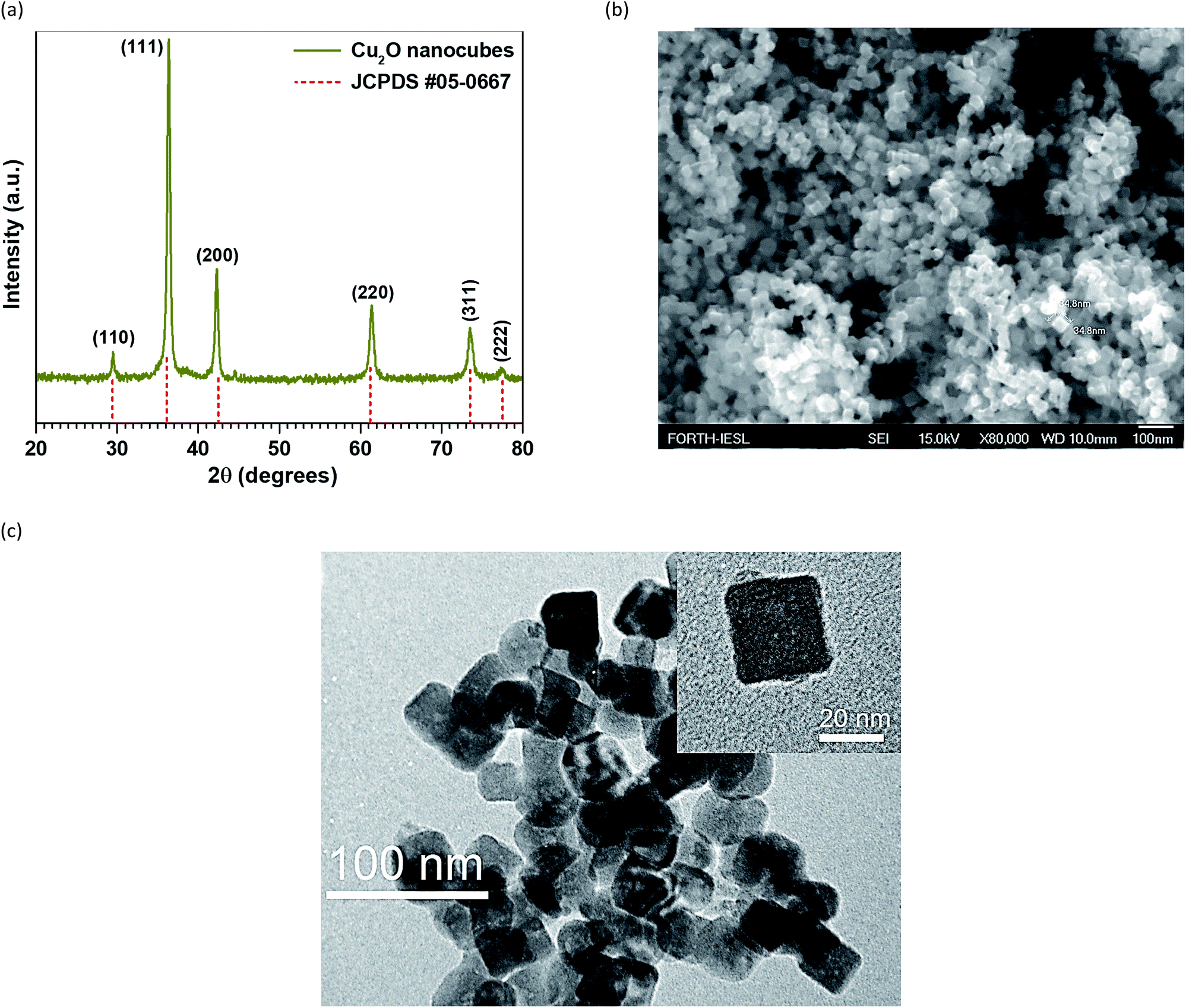 | ||
| Fig. 2 (a) X-ray diffraction (XRD) pattern of Cu2O nanocubes and standard Cu2O card. (b and c) FESEM images and TEM images of Cu2O nanocubes. | ||
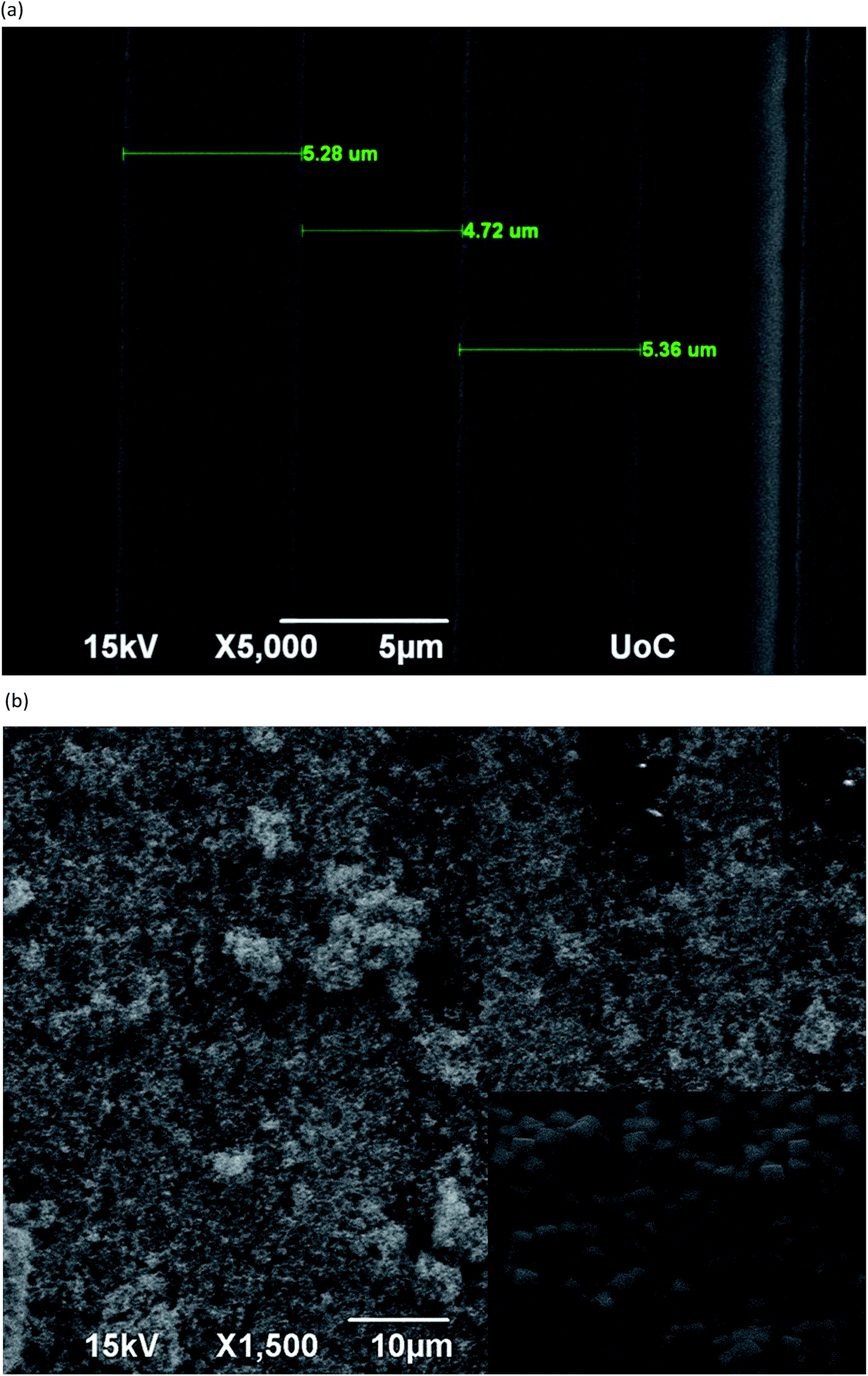 | ||
| Fig. 3 (a) SEM images of the IDEs with a gap of 5 μm. (b) SEM of coated IDEs and zoomed view of the coated IDEs with nanocubes in the inset. | ||
The two-terminal interdigitated sensor devices were tested at room temperature whilst been exposed to different concentrations of ozone in the range 10–820 ppb. The repeatability of the sensing response was also examined by repeating the measurement several times using different Cu2O nanocube-based devices. Fig. 4 shows the evolution of the current (measured at a constant bias of 10 volts) as a function of time and exposure to different ozone concentrations. In particular, the measurement included two steps: (i) the sensor was exposed to an atmosphere containing O3 with a predetermined concentration for approximately 2 min while the current was monitored in real time; (ii) the ozone flow was turned-off and the device was exposed to ambient air (relative humidity ≈ 55%) for approximately 1 min. The same measuring cycle was repeated for O3 concentrations of 170, 490 and 820 ppb (Fig. 4). It is clearly evident that the current across the Cu2O nanocube channel increases in the presence of ozone, an observation consistent with the p-type conductivity in Cu2O nanocubes since an oxidizing gas such as ozone was expected to remove electrons from the top of the valence band of the semiconductor leading to an increased concentration of holes21 – a process that is discussed in details below. Once the ozone flow is turned off and ambient air is re-injected into the test chamber, the current of the Cu2O nanocube channel reduces to almost its original value of ≈0.525 μA (see the current level following exposure to 10 ppb ozone). Although, exposure of the sensor to higher ozone concentrations lead to significantly higher current, the latter does not appear to return to its original value following exposure to ambient air for approximately 1 min. This can be attributed to a residual oxidation caused by the amount of ozone.
 | ||
| Fig. 4 Current changes at room temperature of Cu2O nanocubes due to successive increases in O3 concentrations. | ||
It is clear from the data shown in Fig. 5a that as the O3 concentration increases from 10 to 490 ppb both response (30 s) and recovery times (18 s) of the sensor remain stable, with the only exception being the O3 concentration of 820 ppb where the response time decreased to 24 s and the recovery time increased to 24 s. The gas sensitivity of the sensor as a function of ozone concentration at room temperature is shown in Fig. 5b, from which it can be seen that it is decreased by increasing O3 analytic concentration. The reason for this might be the low working temperature (i.e. 25 °C), compared with previous studies in which a Twork of 175 °C was employed.17 More specifically, this is the first report on the use of Cu2O nanocubes as a self-powered sensing element for the detection of ultra-low O3 concentrations down to 10 ppb with the highest response value of 28% and a response/recovery time of 30/18 s, respectively, at room temperature.
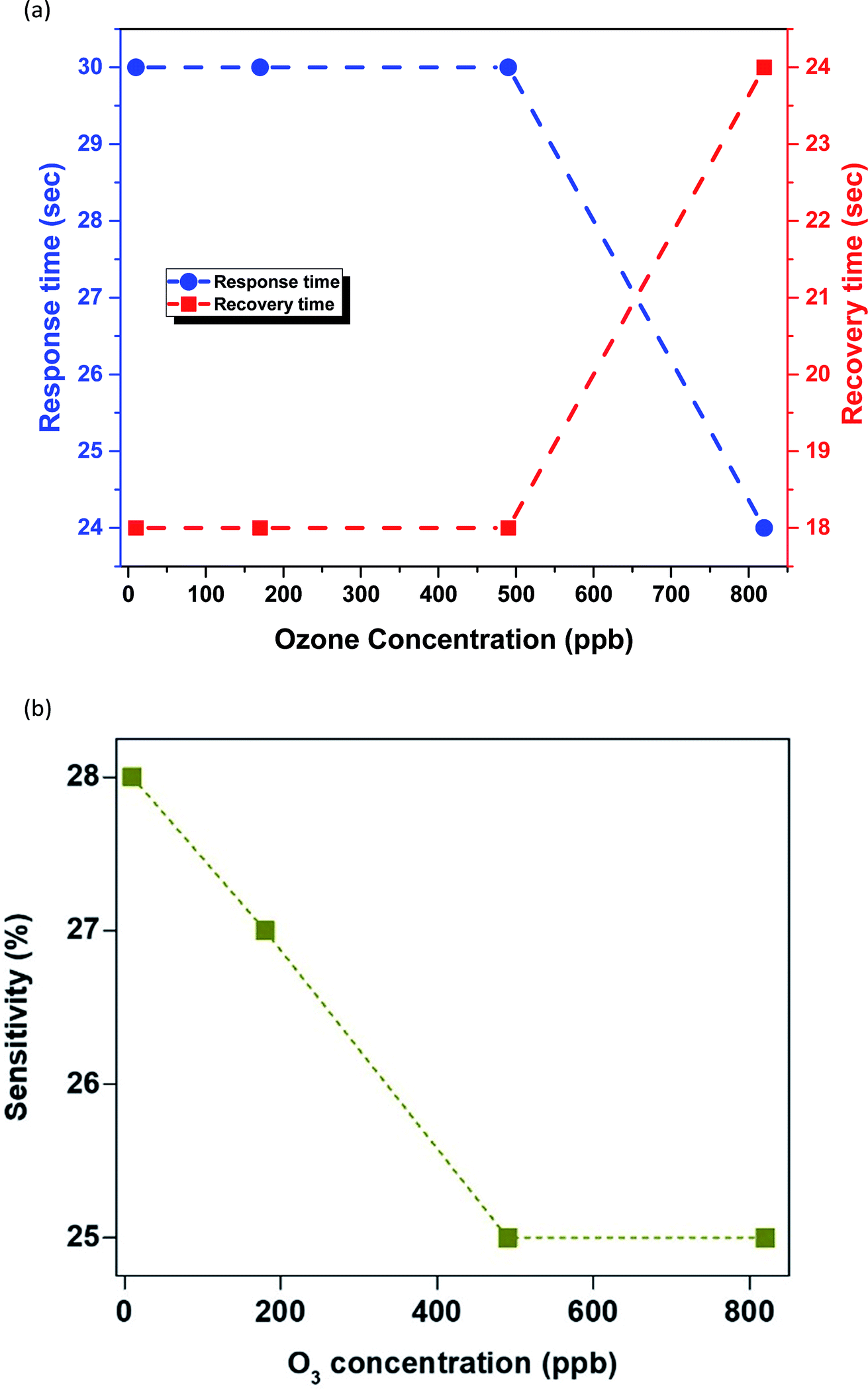 | ||
| Fig. 5 (a) Response and recovery time (s) of the sensor at different ozone concentrations. (b) Sensing sensitivity as a function of ozone concentration. | ||
The experimental data presented so far suggest that O3 species interact with the Cu2O nanocrystals, while this interaction allows the whole process to follow in time the periodic supply of ozone molecules to the sample. In order to elucidate possible atomic-scale mechanisms that underlie the key experimental findings, we performed extensive DFT calculations on the adsorption of O2 and O3 molecules on (001) surfaces, given that (001) facets dominate Cu2O nanocubes,8 while (110) and (111) terminations appear, respectively, only as truncated edges and corners.33
First, we should note that the calculated LUMO value (−5.65 eV) is lower than the measured31 valence band maximum (−5.3 eV) of Cu2O. Hence, any physisorbed O3 species should act as electron acceptors for Cu2O. By the same token, ozone molecules can interact directly with the Cu2O facets. We found that when these facets have low oxygen content (close to the value associated with the stoichiometry of Cu2O), O2 and O3 molecules chemisorb to configurations with large binding energies (in excess of 1.5 eV) and some of the deposited O species move to subsurface sites. Concurrently the Fermi level of the system moves inside its valence band consistent with p-type doping. These results are in agreement with the findings reported by Ouali et al.17
Fig. 6 shows typical steps for the oxidation reactions taking place on Cu2O surfaces with a relatively low O content. First, O2 molecules chemisorb in barrier-less processes and create species like the one shown in the configuration labelled (a) in Fig. 6. Starting from such a chemisorbed configuration, the adsorbed molecule easily breaks into two O adatoms, since the corresponding barrier is only about 0.4 eV. This low activation energy shows that the process takes place even at room temperature. Following the breakup of the molecule, the two O adatoms relax to the intermediate configuration (c) of Fig. 6, and eventually to an even more stable (by about 2 eV) freshly oxidized structure (not shown here). The oxidation reactions with an O3 molecule follow similar steps, namely there is a barrier-less initial chemisorption, followed by an essentially barrier-less breakup of one of the three O atoms of the adsorbed O3 species, and then by reactions akin to those depicted in Fig. 6.
 | ||
| Fig. 6 Energy variation during a typical oxidation reaction on a (001) Cu2O surface. An O2 molecule (its atoms are numbered 1 and 2) chemisorbs with a zero barrier to configuration (a), followed by its breakup to atomic O adatoms and structures (b) and (c). The transition state of the reaction is (b) and the barrier is low and equal to 0.43 eV. | ||
On the other hand, O3 chemisorption continues to take place on areas with increased oxygen content, but in selected such cases, the result is the formation of O3-related defects with relatively low binding energies. Fig. 7 shows two such configurations, an O3-protrusion in Fig. 7a with a single Cu–O bond and an inter-Cu O3-bridge in Fig. 7b. The low binding energies of these O3 configurations (0.90 eV and 0.40 eV, respectively) suggest that when the ozone supply is interrupted, some of the adsorbed O3 species can be replaced by physisorbed O2 molecules which are present in much larger numbers and have corresponding binding energies of 0.23 eV and 0.10 eV. With respect to electronic properties, the results of projected DOS (not shown here) show that the defects shown in Fig. 7 introduce peaks at 0.05 eV and 0.3 eV above the Fermi level of the structure, and hence they can indeed play the role of electron acceptors (though we should note that the thickness of the slab and the use of the PW91 xc-functional do not allow us to draw final conclusions on the exact position of these peaks).
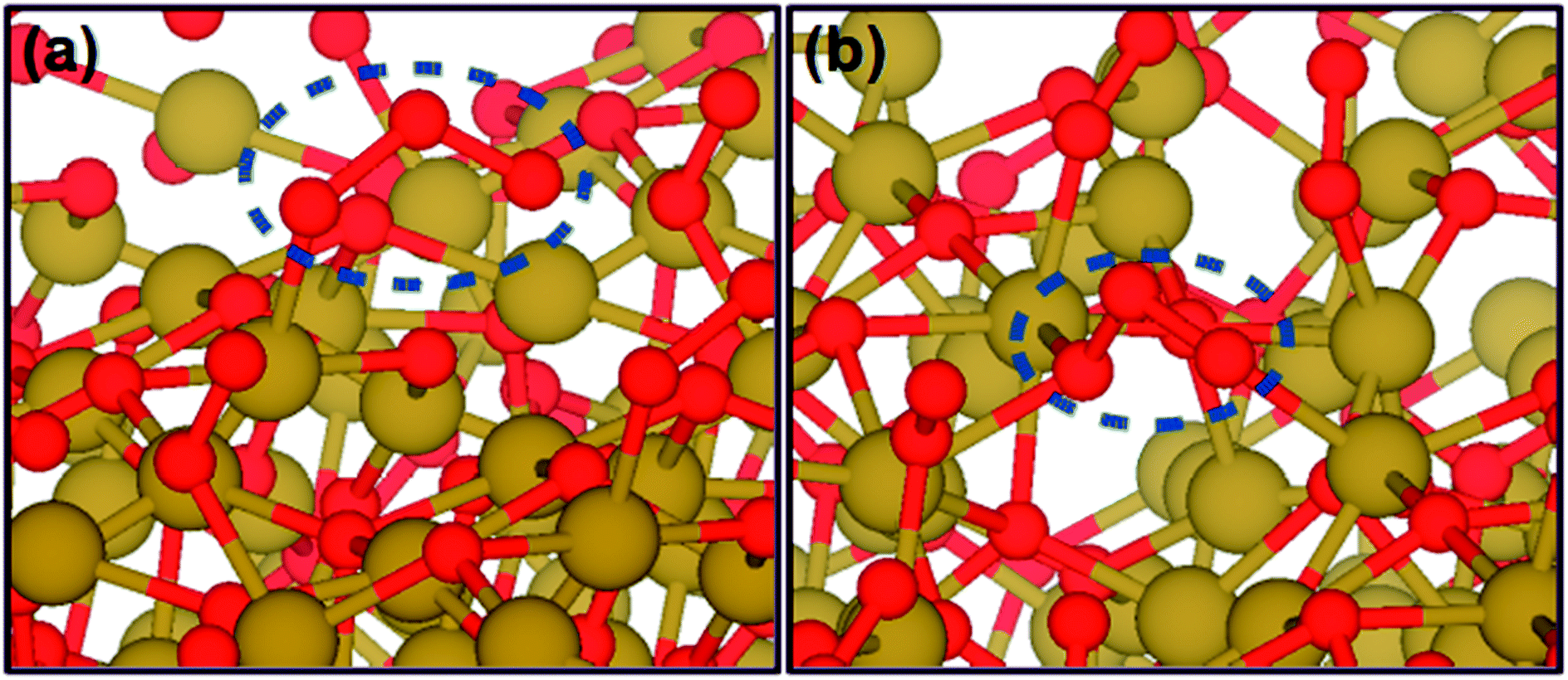 | ||
| Fig. 7 Top views of O3 species over a (001) Cu2O surface: (a) a chemisorbed O3 protrusion (dashed line) with one Cu–O bond. (b) An O3-related bridge (dashed line) between surface Cu atoms. The O3 moiety forms three O–Cu bonds. (Cu: brown, O: red spheres). | ||
The main picture that emerges from these calculations is the following. If Cu2O nanocrystals are not O-rich in the beginning, then the deposition of electronegative oxygen atoms (through, e.g., the dissociation of O3 molecules) contributes to the p-doping of the material. Taking into account also the experimental findings on enhanced hole conductivity, the main reactions during this first stage can be described schematically as:
| Cu2O + O{gas}2 → Cu2O + O{ads}2 → Cu2O + 2O−+2h+ | (3) |
| Cu2O + O{gas}3 → Cu2O + O{ads}3 → Cu2O + 3O−+3h+ | (4) |
When the nanocrystal facets are sufficiently oxidized (a condition which is plausible, but which also depends on the details of growth and operation), then they can selectively trap O3 molecules with binding energies that are neither very large (so that the process may still be reversible) nor very small (so that it can lead to sensing of even small amounts of ozone). This second stage can be described as:
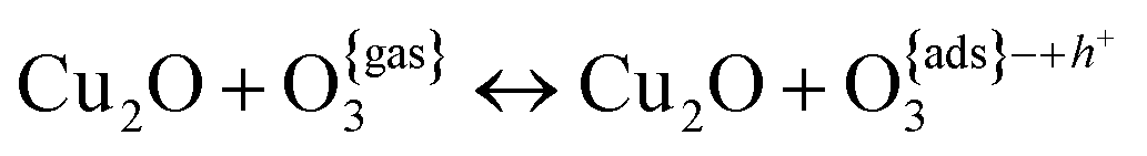 | (5) |
This atomic-scale picture is consistent with the broad features observed in the experiments. Nevertheless, we should stress that the high reactivity of the material (which also results in large local distortions upon oxygen uptake) leaves open the possibility that other adsorption mechanisms may also be important here. Future studies will explore, for example, the role of humidity or of surface reconstructions.
On the basis of the results and analysis presented so far one can argue that there are a few plausible reasons responsible for the fact that the current does not fully recover upon re-exposure of the sensor to ambient air (Fig. 4). The first reason is that the amount of air inserted into chamber for the given recovery (reset) period (∼1 min) is not enough to completely decrease the number of holes that are being created by the adsorption of O3 on Cu2O during the exposure time. Increasing the recovery period would therefore help to reduce the current closer to its original value. Another reason for the incomplete current recovery is dissociation kinetics associated with O3 desorption from the surface of Cu2O at room temperature. This issue could potentially be addressed by operating the sensor at elevated temperature and/or through photo-assisted dissociation albeit at the cost of operational simplicity.
Conclusions
In summary, cuprous oxide nanocubes were successfully synthesized by a solution-based method at room temperature. When the Cu2O nanocubes were incorporated as the sensing element on IDEs, the resulting sensing element showed excellent sensitivity to O3 in the range of 10 to 820 ppb, with fast response and recovery times. Importantly, the self-powered sensing elements of Cu2O nanocubes exhibited a high response (28%) at relatively low ozone concentration (10 ppb) with response and recovery times of 30 and 18 s, respectively. Finally, the p-type nature of the Cu2O nanocubes was confirmed, as the device current was found to increase in the presence of a strongly oxidizing gas, such as ozone.Conflicts of interest
There are no conflicts to declare.Acknowledgements
Current work was supported by COST Action TD1105 “EuNetAir” and by the EU FP7 Program (FP7-REGPOT-2012-2013-1) under grant agreement no. 316165. DFT calculations used computational resources provided by the Bibliotheca Alexandrina (see http://hpc.bibalex.org) and the GRNET HPC facility – ARIS – under projects AFOx and STEM. Part of this work was financially supported by the Stavros Niarchos Foundation within the framework of the project ARCHERS (“Advancing Young Researchers' Human Capital in Cutting Edge Technologies in the Preservation of Cultural Heritage and the Tackling of Societal Challenges”). T. D. A. acknowledges financial support by the King Abdullah University of Science and Technology (KAUST).References
- W. H. O., “Air Quality Guidelines Global Update 2005. Particulate Matter, Ozone, Nitrogen Dioxide and Sulfur Dioxide,” Copenhagen, 2006 Search PubMed.
- X. Wan, J. Wang, L. Zhu and J. Tang, J. Mater. Chem. A, 2014, 2, 13641–13647 RSC.
- F. N. Meng, X. P. Di, H. W. Dong, Y. Zhang, C. L. Zhu, C. Li and Y. J. Chen, Sens. Actuators, B, 2013, 182, 197–204 CrossRef CAS.
- L. Wang, R. Zhang, T. Zhou, Z. Lou, J. Deng and T. Zhang, Sens. Actuators, B, 2016, 223, 311–317 CrossRef CAS.
- L. Wang, R. Zhang, T. Zhou, Z. Lou, J. Deng and T. Zhang, Sens. Actuators, B, 2017, 239, 211–217 CrossRef CAS.
- Y. Sui, Y. Zeng, W. Zheng, B. Liu, B. Zou and H. Yang, Sens. Actuators, B, 2012, 171–172, 135–140 CrossRef CAS.
- L. Gou and C. J. Murphy, Nano Lett., 2003, 3, 231–234 CrossRef CAS.
- C. H. Kuo, C. H. Chen and M. H. Huang, Adv. Funct. Mater., 2007, 17, 3773–3780 CrossRef CAS.
- S. Cao, T. Han, L. Peng, C. Zhao and J. Wang, Ceram. Int., 2017, 43, 4721–4724 CrossRef CAS.
- Q. Cheng, W. Yan, L. Randeniya, F. Zhang and K. Ostrikov, J. Appl. Phys., 2014, 115, 12 Search PubMed.
- J. Liu, S. Wang, Q. Wang and B. Geng, Sens. Actuators, B, 2009, 143, 253–260 CrossRef.
- A. Labidi, H. Ouali, A. Bejaoui, T. Wood, C. Lambert-Mauriat, M. Maaref and K. Aguir, Ceram. Int., 2014, 40, 7851–7856 CrossRef CAS.
- S. T. Shishiyanu, T. S. Shishiyanu and O. I. Lupan, Sens. Actuators, B, 2006, 1, 468–476 CrossRef.
- A. R. Rastkar, A. R. Niknam and B. Shokri, Thin Solid Films, 2009, 517, 5464–5467 CrossRef CAS.
- T. A. P. Pattanasattayavong, S. Thomas, G. Adamopoulos and M. McLachlan, Appl. Phys. Lett., 2013, 102, 163505 CrossRef.
- X. J. N. Tang, B. Chen, Y. Xia and D. Chen, RSC Adv., 2015, 5, 54433–54438 RSC.
- H. Ouali, C. Lambert-Mauriat, L. Raymond and A. Labidi, Appl. Surf. Sci., 2015, 351, 840–845 CrossRef CAS.
- S. Zhou, X. Fang, Z. Deng, D. Li, W. Dong, R. Tao, G. Meng and T. Wang, Sens. Actuators, B, 2009, 143, 119–123 CrossRef.
- Z. Deng, X. Fang, D. Li, S. Zhou, R. Tao, W. Dong, T. Wang, G. Meng and X. Zhu, J. Alloys Compd., 2009, 484, 619–621 CrossRef CAS.
- X. G. Zheng, K. Taniguchi, A. Takahashi, Y. Liu and C. N. Xu, Appl. Phys. Lett., 2004, 85, 1728–1729 CrossRef CAS.
- S. Thirumalairajan, V. R. Mastelaro and C. A. Escanhoela, ACS Appl. Mater. Interfaces, 2014, 21739–21749 CrossRef CAS PubMed.
- C. Baratto, R. Kumar, G. Faglia, K. Vojisavljević and B. Malič, Sens. Actuators, B, 2015, 209, 287–296 CrossRef CAS.
- S. Thirumalairajan and V. R. Mastelaro, Sens. Actuators, B, 2016, 223, 138–148 CrossRef CAS.
- P. Giannozzi, J. Phys.: Condens. Matter, 2009, 21, 395502 CrossRef.
- D. J. G. Kresse, Phys. Rev. B: Condens. Matter Mater. Phys., 1999, 59, 1758–1775 CrossRef.
- C. F. P. Perdew, J. Chevary, S. Vosko, K. Jackson, M. Pederson and D. Singh, Phys. Rev. B: Condens. Matter Mater. Phys., 1992, 46, 6671–6687 CrossRef.
- S. Grimme, J. Comput. Chem., 2006, 27, 1787–1799 CrossRef CAS PubMed.
- M. C. D. Chadi, Phys. Rev. B: Condens. Matter Mater. Phys., 1973, 8, 5747–5753 CrossRef.
- O. A. O. Jepsen, Solid State Commun., 1971, 9, 1763–1767 CrossRef.
- M. Valiev, E. J. Bylaska, N. Govind, K. Kowalski, T. P. Straatsma, H. J. J. Van Dam, D. Wang, J. Nieplocha, E. Apra, T. L. Windus and W. A. de Jong, Comput. Phys. Commun., 2010, 181, 1477–1489 CrossRef CAS.
- H. A. S. Wilson, J. Bosco, Y. Tolstova, D. Scanlon and G. Watson, Energy Environ. Sci., 2014, 3606–3610 RSC.
- A. D. Becke, J. Chem. Phys., 1993, 98, 5648–5652 CrossRef CAS.
- L. I. Bendavid and E. A. Carter, J. Phys. Chem. B, 2013, 117, 15750–15760 CrossRef CAS.
| This journal is © The Royal Society of Chemistry 2019 |