
 Open Access Article
 This Open Access Article is licensed under a Creative Commons Attribution-Non Commercial 3.0 Unported Licence
Analysis of nonlinear characteristics of a graphene based four-terminal ballistic rectifier using a drift-diffusion model
Ankur
Garg
 a,
Neelu
Jain
a,
Sanjeev
Kumar
b,
Shahrir R.
Kasjoo
c and
Arun Kumar
Singh
*a
a,
Neelu
Jain
a,
Sanjeev
Kumar
b,
Shahrir R.
Kasjoo
c and
Arun Kumar
Singh
*a
aDepartment of Electronics and Communication Engineering, Punjab Engineering College (Deemed to be University), Sector-12, Chandigarh-160012, India. E-mail: arun@pec.ac.in
bDepartment of Applied Sciences, Punjab Engineering College (Deemed to be University), Sector-12, Chandigarh-160012, India
cSchool of Microelectronic Engineering, Universiti Malaysia Perlis, 02600 Arau Perlis, Malaysia
First published on 9th September 2019
Abstract
In this study, rectification behavior and noise spectra of a graphene based four-terminal ballistic rectifier are reported utilizing semi-classical drift-diffusion 3D modeling. The room temperature DC and RF characteristics of the novel rectifier are demonstrated considering the traps in the material similar to a real device, reducing the rectification efficiency from 0.5% to 0.35%. The responsivity and noise equivalent power of about 89.21 mV mW−1 and 97.52 pW Hz−1/2, respectively, are obtained for different frequencies varying from 50 Hz to 1 THz. Furthermore, the noise spectral analysis of the device predicts a minimum low frequency noise, which depends upon the carrier concentration inside the device active region rather than mobility, and hence enables potential applications as THz detectors for imaging.
Introduction
Graphene is a zero band gap material with a typical mobility of up to 200![[thin space (1/6-em)]](https://www.rsc.org/images/entities/char_2009.gif) 000 cm2 V−1 s−1,1 and mean free length (λMFL) in the μm range at room temperature.2 However, most electronic devices require a band gap and are not able to take advantage of high carrier mobility in single layer graphene, for example, nano-ribbons3 and tunneling transistors.4 Further, graphene can be encapsulated with hexagonal boron nitride (h-BN) to provide a smooth surface in comparison to SiO2.5 This enhances the surface flatness and generates a lower number of scattering events and interface traps. During the last decade, many ballistic devices have been reported with III–V heterostructures6,7 which take advantage of high mobility and large λMFL (140 nm to 6 μm from 300 to 4.2 K).8 The characteristic length of these devices is smaller than λMFL which produces ballistic effects in the active region. These devices are the three-terminal junction (TTJ),9–11 four-terminal ballistic rectifier (FTBR),12,13 and ballistic deflection transistor (BDT).14,15
000 cm2 V−1 s−1,1 and mean free length (λMFL) in the μm range at room temperature.2 However, most electronic devices require a band gap and are not able to take advantage of high carrier mobility in single layer graphene, for example, nano-ribbons3 and tunneling transistors.4 Further, graphene can be encapsulated with hexagonal boron nitride (h-BN) to provide a smooth surface in comparison to SiO2.5 This enhances the surface flatness and generates a lower number of scattering events and interface traps. During the last decade, many ballistic devices have been reported with III–V heterostructures6,7 which take advantage of high mobility and large λMFL (140 nm to 6 μm from 300 to 4.2 K).8 The characteristic length of these devices is smaller than λMFL which produces ballistic effects in the active region. These devices are the three-terminal junction (TTJ),9–11 four-terminal ballistic rectifier (FTBR),12,13 and ballistic deflection transistor (BDT).14,15
The ballistic rectifier is a four-terminal device, and its working resembles the operation of a p–n diode based bridge rectifier.12 In contrast to the bridge rectifier, the FTBR does not rely on any built-in potential and starts operating from non-zero input potential. In addition, this device does not require any band gaps to make it operational; hence it is favorable to use single layer graphene as an active layer. The planar structure and in-plane contact configuration generate less parasitic capacitance which enhances the speed of the FTBR up to THz frequencies.16 A triangular antidot intentionally placed in the center of the FTBR provides asymmetry to the device structure. Furthermore, the antidot deflects a large number of carriers toward the lower terminal and is responsible for the rectification. Previously, these devices have been fabricated using 2DEG materials such as GaAs and InGaAs to work up to a frequency of 50 GHz experimentally17 and have predicted the operation up to THz frequencies using Monte-Carlo (MC) simulations.6 Other devices such as artificial nanomaterials18 and TTJs9–11 have also been reported to generate a rectified output. The BDT, which is the modification of the FTBR, is demonstrated to perform digital operations including a NAND gate.8,19 The nonlinear response of the FTBR can be explained using an extended Landauer–Büttiker approach, where transmission probability of charge carriers and the electrochemical potential difference between terminals are considered for predicting rectified DC outputs.20 In addition, the billiard ball transport model has been used strategically for the deflection of charge carriers toward output terminals using the triangular antidot.20,21 The potential applications of the FTBR include energy harvesting,5 frequency doubling,22 voltage inversion, and THz imaging.23
Single layer graphene can be transferred on different substrates such as SiO2 and h-BN by exfoliation. The substrate used is responsible for different graphene properties including mobility and hence λMFL. For the first time, graphene FTBR fabrication was reported using a SiO2 substrate with the mobilities of 1572 and 1872 cm2 V−1 s−1 for holes and electrons, respectively.24 Here, the SiO2 substrate provided a rough surface to graphene which created puddles and was responsible for the lower mobility. Recently, the graphene FTBR is fabricated on the h-BN substrate providing higher mobility (200000 cm2 V−1 s−1) and longer λMFL (1 μm).21 The utilization of h-BN as the encapsulated layer provides a flat surface to the active graphene layer and eliminates the traps that generate high mobility charge carriers. In order to reduce significant cost in experiments for the optimization of the device geometry, simulations are typically being used. Recently, the simulation and modeling of graphene based TTJ rectifiers have been reported, considering a carrier mobility of 4000 cm2 V−1 s−1 to compare the simulated results with the reported data.11,25
The simulations are typically being utilized for device geometry optimization and hence reduce the significant cost of an experiment. However, no simulation effort has been made on the graphene FTBR until now. Thus in this work, a simulation study along with noise analysis of the graphene FTBR with a triangular antidot is performed and validated with the equivalent resistor network. The DC and RF characteristics are analyzed in combination with trap effects at room temperature and THz frequency. Previously, only two dimensional (2D) MC simulations of InGaA based nanodevices have been performed where the front and top view of the device was considered separately.6 In contrast, three dimensional (3D) simulations in addition to 2D simulations are reported and compared in this work, which is a more accurate approach. In addition, the high frequency (THz) operating capability of the FTBR is validated with the responsivity and noise equivalent power (NEP) characteristics. Furthermore, the low frequency behavior of the FTBR is also simulated with an equivalent 2D structure and is validated with the theory.
Modeling of the graphene FTBR
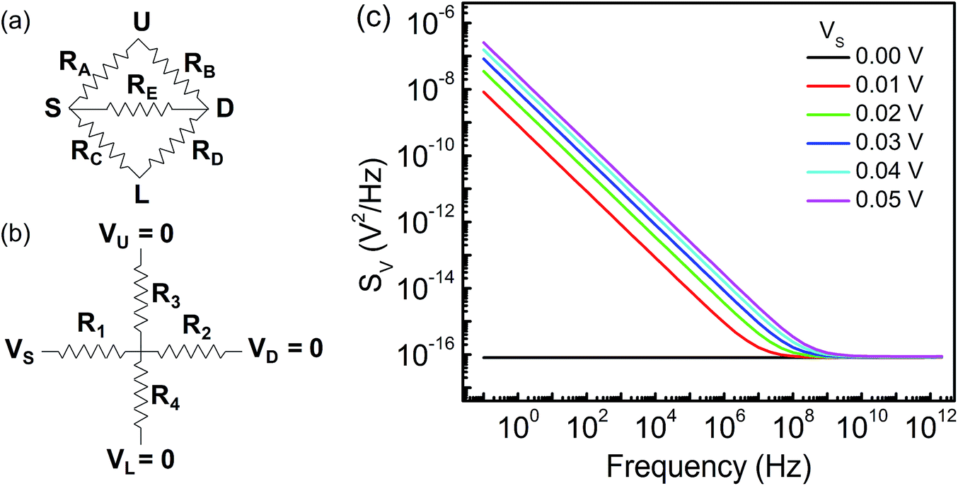
The FTBR as shown in Fig. 1(a) is simulated using single layer graphene with a thickness of 0.35 nm, and a highly doped Si/SiO2 substrate with a dielectric thickness (t) and permittivity (ε) of 285 nm and 3.9, respectively. The models for the graphene based structure are validated with a carrier mobility (μ) of 4000 cm2 V−1 s−1,25 which corresponds to λMFL = (h/2e)μ(ns/π)1/2 of 39 nm.24 Here, h is the Planck's constant and e is the electron charge. The carrier density for graphene is estimated with a parallel plate capacitor model using ns = ε0εVG/te, where ε0 is the free space permittivity and VG is the back gate voltage.26 As seen from Fig. 1(a), the device active region of the proposed ballistic rectifier has an antidot (triangular structure) at the center which deflects the charge carriers either originated from the source (S) or drain (D) terminal to the lower (L) terminal. The length of the upper side wall of the antidot triangle is 30 nm and the available channel lengths between upper and source/drain terminals are 35 nm each which is less than the mean free path length of 39 nm. However, the overall length of the device is 250 nm which is larger than the mean free path length. Hence, the drift-diffusion model is utilized to compute/estimate the electrical characteristics of the device analogous to the approach utilized for evaluating the electrical characteristics of the InGaA based ballistic rectifier implementing Monte Carlo simulations.6,7 Silvaco Atlas software is used for modeling and simulation of the graphene FTBR, in which Poisson's and continuity equations are used for a general framework to co-relate the electrostatic potential with the charge density.27 Also, the continuity equation is used in combination with transport equations for carrier densities considering various effects such as generation and recombination of carriers, and transport processes.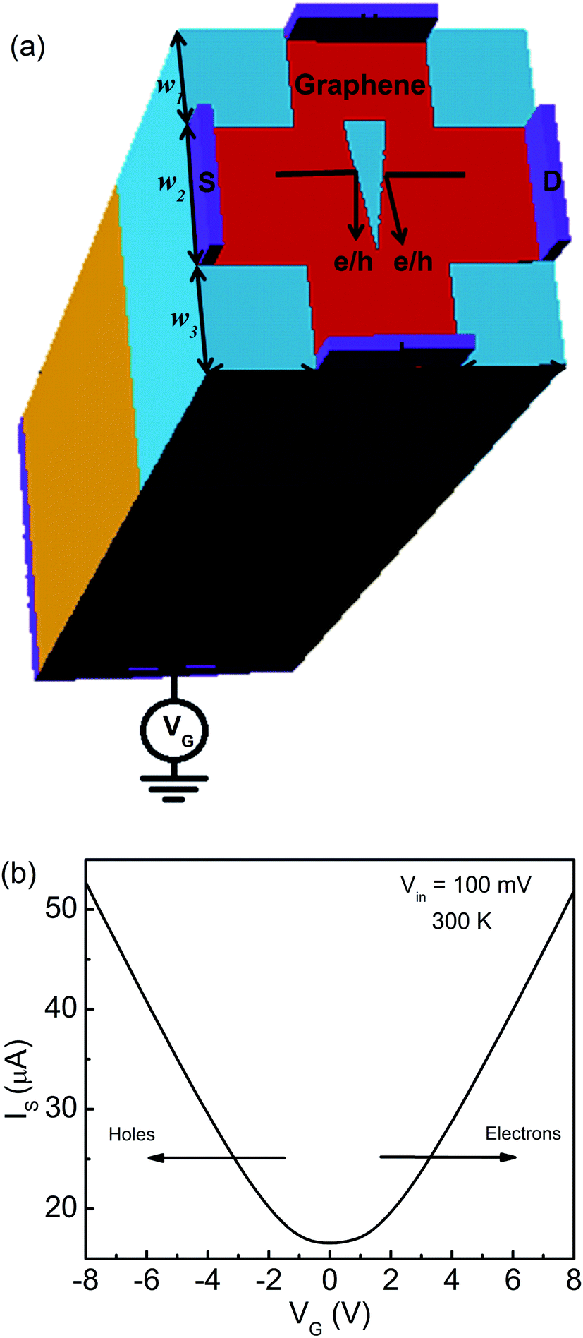 | ||
| Fig. 1 (a) 3D device structure of the graphene FTBR with a highly doped Si/SiO2 substrate. The triangular antidot at the centre of the device deflects a large number of electrons and/or holes toward the lower terminal as indicated by arrows. The dimensions are l1 = l3 = w1 = w3 = 75 nm and l2 = w2 = 100 nm. The FTBR terminals are source (S), drain (D), lower (L), and upper (U). The rectified response is generated between L and U terminals when a non-zero input is applied between S and D terminals. (b) The transfer characteristic of the FTBR shows input branch current (IS) as a function of applied back gate voltage (VG) for a push–pull input voltage of 100 mV between S and D terminals in push–pull (PP) configuration. | ||
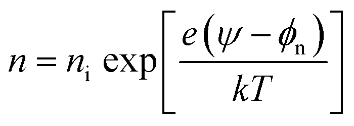
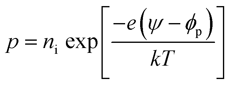
The drift-diffusion model25 is used to calculate the current densities Jn and Jp, and carrier concentrations n and p for electrons and holes, respectively, which depend on quasi-Fermi levels denoted by φn and φp.
| Jn = −eμnn∇φn | (1) |
| Jp = −eμpp∇φp | (2) |
 | (3) |
 | (4) |
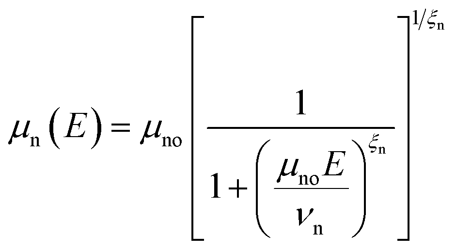
The field dependent mobility model is used to formulate the effective mobility of carriers and is given as
 | (5) |
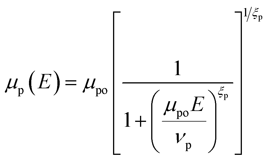 | (6) |
The parameters μno and μpo are the low-field carrier mobilities and can be calculated using
 | (7) |
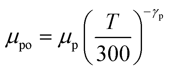 | (8) |
The intrinsic carrier concentration can be calculated using
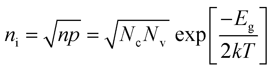 | (9) |
For single layer graphene, the band gap (Eg) is considered to be zero; therefore eqn (9) can be written as
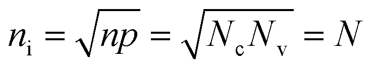 | (10) |
The parallel plate capacitor model is used to calculate the surface charge density of graphene which is normalized into the density of states (N) using graphene thickness. It shows a similar value calculated using the Fermi integral of order 1 with intrinsic carrier concentration and is given as25,28
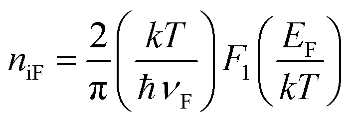 | (11) |
The value of F1 cannot be integrated analytically; therefore, the following approximations are used to calculate the intrinsic carrier concentration such as EF = 0 and F1 = π2/12 and carrier concentration becomes28
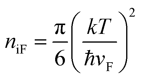 | (12) |
The value of niF can be calculated for different temperatures using eqn (12).
Results and discussion
Three dimensional (3D) structure and simulation
The FTBR is designed on single layer graphene having four-terminals, source (S), drain (D), lower (L), and upper (U), as demonstrated in Fig. 1(a). A triangular antidot is intentionally placed at the center of the device to provide asymmetry between output terminals and deflect a large number of electrons and/or holes toward the L terminal as compared to the U terminal. The Si/SiO2 substrate is back gated with an electrode that can tune the type of charge carriers in the graphene layer from electrons to holes and vice versa. The collimation of charge carriers inside the channel is dominating which changes the transmission probability of electrons/holes between the input (S and D) and output (L and U) terminals and results in the rectified output.20 The transfer characteristic of the FTBR for an input voltage of 100 mV in push–pull (PP) configuration demonstrating the zero Dirac point considering ideal graphene is shown in Fig. 1(b), and the voltage (VG) is applied on the back gate electrode. The left and right sides of the curve demonstrate hole and electron dominant regions, respectively.The output response of the FTBR as a function of VG is shown in Fig. 2(a). The traps with a charge density of 0.1 × 1012 cm−2 are considered to simulate the real device like characteristics at room temperature; however at the lower temperature, the traps become frozen out and hence are not considered.25 The rectification is reduced from 0.5% to 0.35% with traps at 300 K. Furthermore, the efficiency of the device is increased more than three times (1.86%) at 77 K and more than six times (3.17%) at 4 K as shown in Fig. 2(b). At lower temperature, the λMFL and mobility of the device increase, improving the rectification efficiency. In addition, the rectification efficiency of the FTBR can further be improved by fabricating graphene with a smooth surface and edges which in turn increases the mobility of the device.24
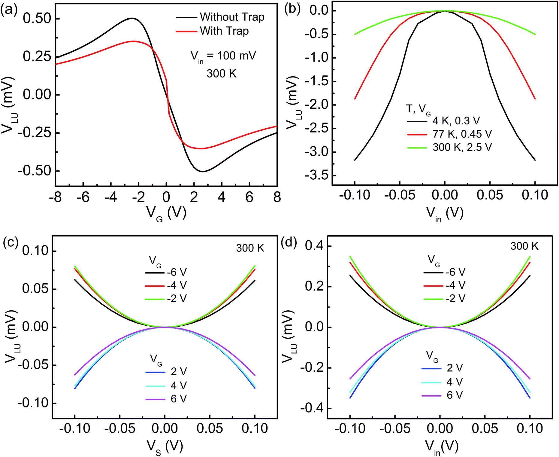 | ||
| Fig. 2 (a) The output response of the FTBR with and without traps for different values of VG. (b) Input-output response of the rectifier at different temperatures. The FTBR is biased using (c) push-fixed (PF) and (d) PP input configurations. Both the input configurations are simulated for electrons (downward) and holes (upward) at different VG. The rectifier can be used as a voltage inverter by changing the VG from positive to negative and vice versa. | ||
The output response of the device is simulated for two input voltage configurations such as push-fixed (PF) and PP for different VG as shown in Fig. 2(c) and (d), respectively. The nonlinear output is related to the non-zero input as29
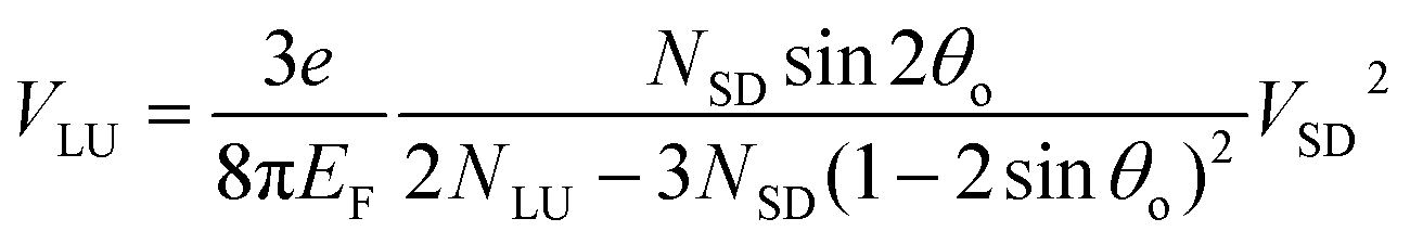 | (13) |
Eqn (13) shows the quadratic relationship between the input and output voltages and can be further reduced to VLU = ±αVSD2, where α is the curvature of the curve (−α for electrons and +α for holes). Both PF and PP input configurations can be extracted from each other. The output in PF input configuration at VS = 2Vin and VD = 0 is equal to the output in PP input configuration at Vin = VS = −VD, where VS and VD are the source and drain voltages, respectively, and Vin is the PP input voltage. Both the input configurations demonstrate the rectifier function as a voltage inverter by switching the charge carriers from electrons to holes and vice versa using VG. In addition, the Fermi levels of S and D terminals are changed when the input is applied; as a result, charge carriers start flowing from one terminal to another terminal. Due to the presence of the triangular antidot, more number of charge carriers deflect toward the L terminal. Accordingly, the charge carrier difference between L and U terminals generates the rectified DC output (VLU).
The AC response of the graphene FTBR in pp configuration is simulated at 1 KHz as shown in Fig. 3(a). The DC rectified output demonstrates device operation as a frequency doubler. Furthermore, the back gate electrode affects the FTBR efficiency largely and switches the carriers for conduction. Therefore the speed of the ballistic rectifier is required to be confirmed at different VG using responsivity and NEP characteristics as shown in Fig. 3(b) and (c), respectively. The responsivity measures the speed in terms of output voltage generated by a rectifier in response to the applied input power and NEP is the ratio of thermal voltage to the responsivity of the device. The ballistic rectifier generates the thermal noise voltage of 8.7 nV Hz−1/2 corresponding to the equivalent resistance R3D of 4.57 KΩ calculated using  . The device demonstrates a responsivity of up to 88.89 mV mW−1 and NEP of 97.87 pW Hz−1/2 at a VG of −2 V. The very first graphene based four terminal ballistic rectifier on the SiO2 substrate demonstrated a responsivity of about 66.68 mV mW−1 and NEP in the order of 10−9 W Hz−1/2 with a carrier mobility of 1872 cm2 V−1 s−1.24 However, recent experiments on the graphene based FTBR utilizing the h-BN substrate exhibiting a carrier mobility of 200000 cm2 V−1 s−1 have demonstrated the significant improvement (>300 times) in the responsivity of 23000 mV mW−1 and NEP as low as 0.64 pW Hz−1/2.21 This further suggests that the device detection sensitivity and NEP improve with the increase in carrier mobility ensuring purely ballistic transport. In addition, it is worth mentioning that the NEP of graphene based ballistic rectifiers is comparable to that of commercially available uncooled terahertz detectors e.g. bolometers, Goley cells etc.24 These values can be further improved by optimizing the device dimensions and utilizing a substrate that provides better mobility in the graphene layer. Furthermore, the device responds well up to a frequency of 1 THz as demonstrated in Fig. 3(d). The graphene FTBR is expected to operate up to much higher frequencies by carefully designing the device with matched input–output impedance to ensure maximum power transfer between input and output terminals.
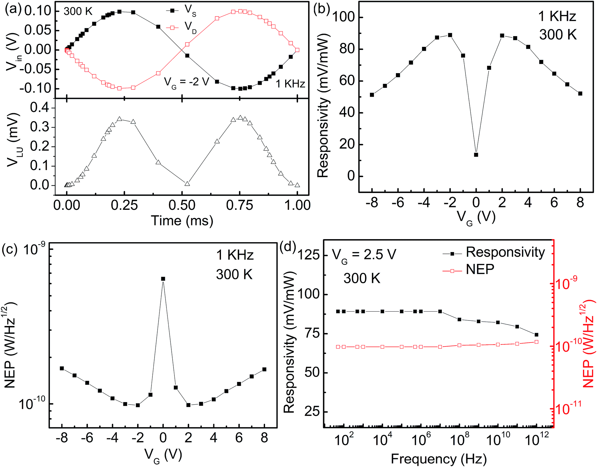 | ||
| Fig. 3 (a) AC characteristics of the FTBR simulated at 1 KHz for VS = −VD = 0.1 V PP configuration demonstrate the device working as a frequency doubler. The RF performance of the rectifier is demonstrated using (b) responsivity and (c) NEP at different VG for electrons and holes, respectively. Similarly, the speed of the device is validated in (d) by increasing the frequency up to the THz range. | ||
Two dimensional (2D) structure and simulation
The 2D structure of the ballistic rectifier is developed using a single layer of graphene and the results are compared with 3D simulations. Fig. 4(a) and (b) show the 2D structure of the FTBR with PF and PP input configurations, respectively. The approach required to analyze the noise behaviour of the FTBR as a 3D noise simulator is not available. Previously, the 2D approach was reported to simulate the III–V material ballistic device without considering the 3D geometry.6,7 Instead, here 3D and 2D geometries are simulated separately, and their results are compared, which is a more accurate approach.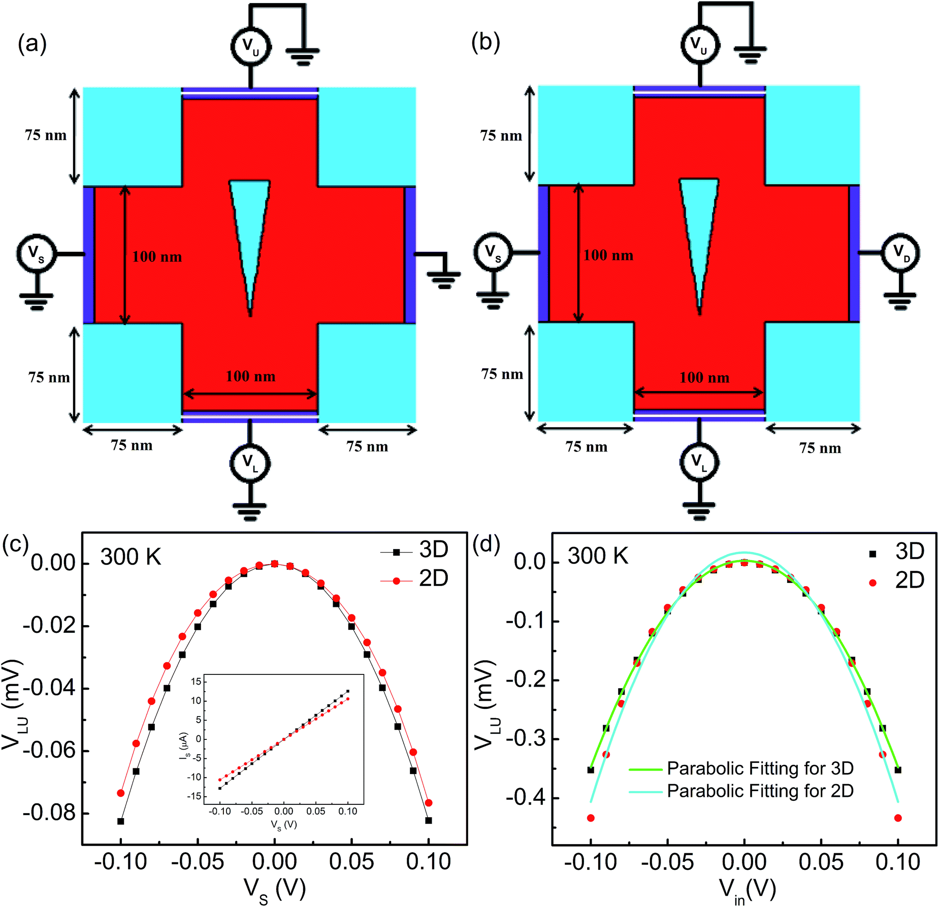 | ||
| Fig. 4 Device active region is simulated in two dimensional (2D) for PF (a and c) and PP (b and d) input configurations. The input–output response of the ballistic rectifier is optimized and compared for VG = 2.5 V. The PP response of the rectifier is according to the rectified response of the device VLU = ±αVSD2, as shown by parabolic fitting. | ||
In PF configuration, the input is applied either from the S or D terminal (VS = 2Vin and VD = 0) at VG = 2.5 V and rectified response is measured between L and U terminals as shown in Fig. 4(c). In PP configuration as shown in Fig. 4(d), the input is applied between S and D terminals (Vin = VS = −VD) at VG = 2.5 V and rectified response is measured between L and U terminals. The 3D and 2D responses of the ballistic rectifier are parabolic (VLU = ±αVSD2) as given in eqn (13), where α is equal to −0.0351 and −0.0423 V−1, respectively, which is calculated using quadratic curve fitting. Furthermore, the optimized 2D geometry is used to analyze the noise behaviour of the ballistic rectifier.
Noise analysis of the FTBR
The FTBR has zero intrinsic threshold which eliminates the use of a biasing circuit even at higher frequencies. In addition, output terminals in the FTBR are orthogonal to input terminals, which offer less noise as compared to the conventional p–n diode.21 However, the analysis of low frequency noise is required as in RF design it translates into the phase noise at higher frequencies.30 The 2D structure of the ballistic rectifier is simulated for noise spectra from 0.1 Hz to 1 THz frequency. The equivalent resistor network of the rectifier is demonstrated in Fig. 5(a), where resistance between any two terminals is calculated by taking other terminals as the open circuit represented by RA, RB, RC, RD and RE. The resistor network in Fig. 5(b) can be extracted such that RE = R1 + R2 and RA = RB = RC = RD = R1 + R3 = R2 + R4.31 The ballistic rectifier generates a thermal noise resistance (R2D) of 4.88 KΩ that is in good agreement with the resistor network of value 5.7 KΩ. Furthermore, the thermal noise calculated from 2D noise simulation of the FTBR is 8.99 nV Hz−1/2 which is in good accordance with a 3D thermal noise of 8.7 nV Hz−1/2.
 | ||
| Fig. 5 (a and b) Equivalent resistive network of the graphene FTBR. (c) Noise spectra of the ballistic rectifier are simulated from the S terminal of the device for different values of input voltages. The thermal noise is generated at Vs = 0 V that matched with the resistance calculated from the resistor network. Fitting of noise spectra results in β = 1 ± 0.001 which is in analogous with the Hooge's theory. | ||
The traps are inherently present in the structure due to the rough surface provided by the SiO2 substrate which decreases the mobility of charge carriers in the graphene layer and directly affects the number of carriers generating low frequency noise. The spectral density of low frequency noise is inversely proportional to applied signal frequency and is known as flicker noise or 1/f noise. The flicker noise can be formulated using Hooge's relation given below:30,32
 | (14) |
The spectral density of the FTBR for different input voltages is shown in Fig. 5(c). The curve at higher voltage coincides with the thermal noise at MHz frequencies. Also, the noise spectra are directly proportional to the square of applied voltage according to eqn (14). In addition, the noise spectra also vary with the number of factors including the Hooge's constant (αH) and number of charge carriers (NT). The charge carriers and mobility are related to each other as given by the conductivity (σ) or resistivity (ρ) expression as
 | (15) |
The spectral density is simulated for different values of αH (up to three orders of magnitude) which demonstrate change in the 1/f noise as shown in Fig. 6(a). The mobility variations did not affect flicker noise but suggest the change in thermal noise due to the change in device resistance as shown in Fig. 6(b).
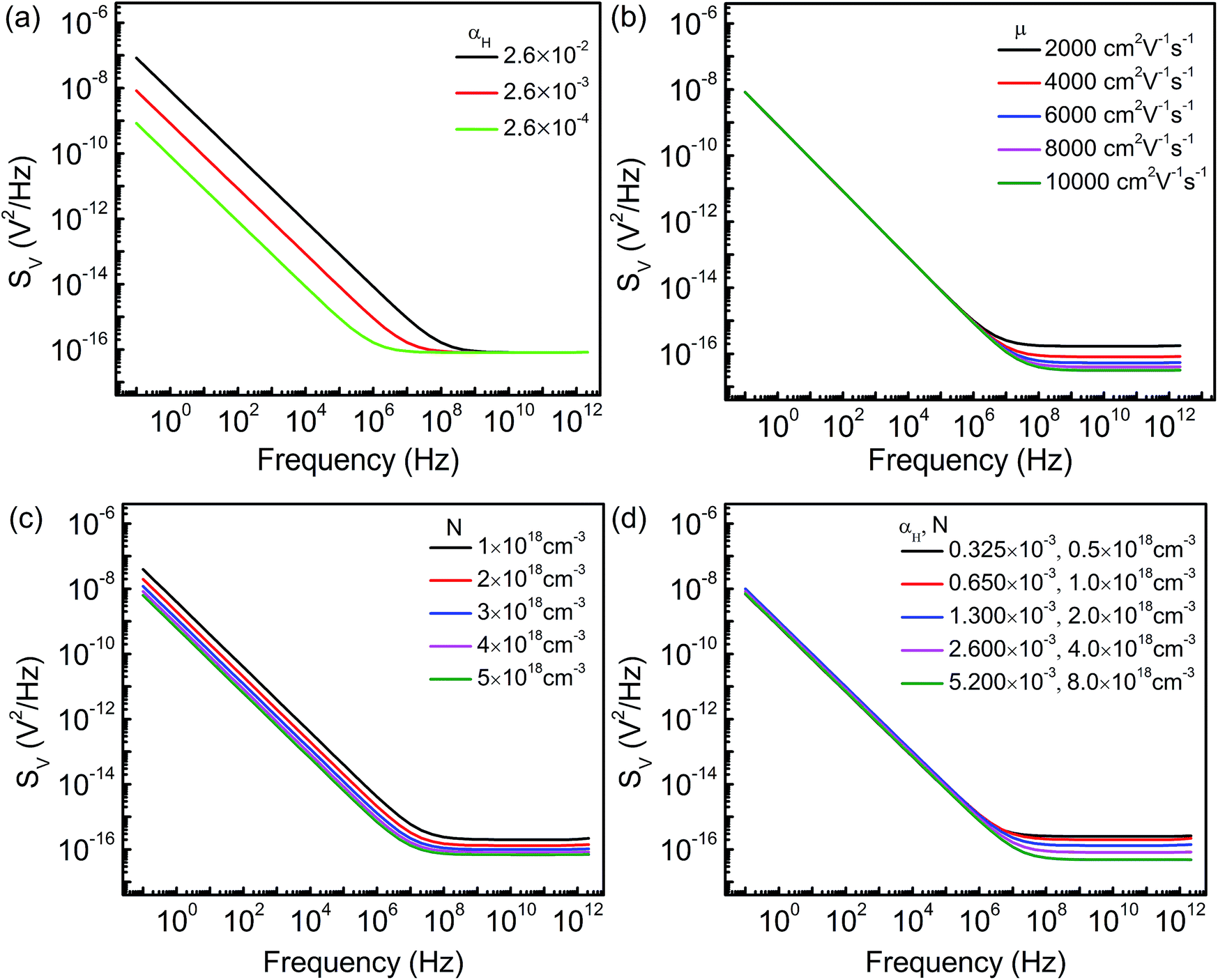 | ||
| Fig. 6 (a) The simulated noise spectra of the FTBR for different αH orders demonstrating the effect on the flicker noise (μ = 4000 cm2 V−1 s−1; N = 4 × 1018 cm−3). (b) The mobility variations in the device channel do not affect the flicker noise, but change the thermal noise (αH = 2.6 × 10⁻³; N = 4 × 1018 cm−3). (c) Both the flicker and thermal noise of the ballistic rectifier are varied with the change in the number of charge carriers in the channel (αH = 2.6 × 10⁻³; μ = 4000 cm2 V−1 s−1). (d) Similar phenomenon is observed by changing αH and N with the same amplitude, where flicker noise is not affected due to equal change in αH and N (μ = 4000 cm2 V−1 s−1). | ||
In addition, the number of charge carriers is varied as shown in Fig. 6(c), which affects both the flicker noise and device resistance according to eqn (14) and (15). The results suggest that the flicker noise is due to the fluctuation in carrier concentration rather than mobility. The effect of carrier fluctuation on 1/f noise can be minimized by utilizing a suitable material having appropriate αH as shown in Fig. 6(d).
Conclusions
The graphene FTBR is simulated using the drift-diffusion model. The obtained results for 3D and 2D geometries are compared with each other for PF and PP input configurations. The device demonstrates a responsivity and NEP of 89.21 mV mW−1 and 97.52 pW Hz−1/2, respectively. The noise characteristics of the graphene FTBR suggest that the device exhibits low frequency noise, which is mainly due to the number of charge carriers available in the channel, and is not affected by mobility. In addition, the device speed can be enhanced by producing graphene on a suitable substrate having properties without affecting low frequency noise. Accordingly, the graphene ballistic rectifier can be used as a room temperature detector at high microwave/terahertz frequencies producing a high rectification ratio similar to a graphene self-switching device33 for various applications including THz imaging.Conflicts of interest
There are no conflicts to declare.Acknowledgements
This work was supported by the Science and Engineering Research Board (SERB), Department of Science and Technology (DST), Govt. of India (SB/S3/EECE/002/2016). AG acknowledges financial support from Punjab Engineering College (Deemed to be University), Chandigarh, India.References
- K. I. Bolotin, K. J. Sikes, Z. Jiang, M. Klima, G. Fudenberg, J. Hone, P. Kim and H. L. Stormer, Solid State Commun., 2008, 146, 351–355 CrossRef CAS.
- K. S. Novoselov, V. I. Fal'ko, L. Colombo, P. R. Gellert, M. G. Schwab and K. Kim, Nature, 2012, 490, 192–200 CrossRef CAS PubMed.
- M. Y. Han, B. Özyilmaz, Y. Zhang and P. Kim, Phys. Rev. Lett., 2007, 98, 206805 CrossRef PubMed.
- L. Britnell, R. V. Gorbachev, R. Jalil, B. D. Belle, F. Schedin, A. Mishchenko, T. Georgiou, M. I. Katsnelson, L. Eaves, S. V. Morozov, N. M. R. Peres, J. Leist, A. K. Geim, K. S. Novoselov and L. A. Ponomarenko, Science, 2012, 335, 947–950 CrossRef CAS PubMed.
- G. Auton, R. K. Kumar, E. Hill and A. Song, J. Electron. Mater., 2017, 46, 3942–3948 CrossRef CAS.
- J. Mateos, B. G. Vasallo, D. Pardo, T. Gonzalez, J. Galloo, S. Bollaert, Y. Roelens and A. Cappy, IEEE Trans. Electron Devices, 2003, 50, 1897–1905 CrossRef CAS.
- J. Mateos, B. G. Vasallo, D. Pardo, T. González, J. S. Galloo, Y. Roelens, S. Bollaert and A. Cappy, Nanotechnology, 2003, 14, 117 CrossRef CAS.
- V. Kaushal, I. Iñiguez-de-la-Torre and M. Margala, Solid-State Electron., 2011, 56, 120–129 CrossRef CAS.
- H. Q. Xu, Appl. Phys. Lett., 2001, 78, 2064–2066 CrossRef CAS.
- A. Jacobsen, I. Shorubalko, L. Maag, U. Sennhauser and K. Ensslin, Appl. Phys. Lett., 2010, 97, 032110 CrossRef.
- P. Butti, I. Shorubalko, U. Sennhauser and K. Ensslin, J. Appl. Phys., 2013, 114, 033710 CrossRef.
- A. M. Song, A. Lorke, A. Kriele, J. P. Kotthaus, W. Wegscheider and M. Bichler, Phys. Rev. Lett., 1998, 80, 3831–3834 CrossRef CAS.
- A. M. Song, Encycl. Nanosci. Nanotechnol., 2004, 9, 371–389 CAS.
- Q. Diduck, M. Margala and M. Feldman, IEEE MTT-S Int. Microw. Symp. Dig., IEEE, 2006 Search PubMed.
- Q. Diduck, H. Irie and M. Margala, Int. J. High Speed Electron. Syst., 2009, 19, 23–31 CrossRef CAS.
- A. K. Singh, S. R. Kasjoo and A. M. Song, IEEE Trans. Nanotechnol., 2014, 13, 527–531 CAS.
- A. M. Song, Appl. Phys. A, 2002, 75, 229–235 CrossRef CAS.
- A. M. Song, P. Omling, L. Samuelson, W. Seifert, I. Shorubalko and H. Zirath, Appl. Phys. Lett., 2001, 79, 1357–1359 CrossRef CAS.
- D. Wolpert, Q. Diduck and P. Ampadu, IEEE Trans. Nanotechnol., 2009, 10, 150–154 Search PubMed.
- A. M. Song, Phys. Rev. B: Condens. Matter Mater. Phys., 1999, 59, 9806–9809 CrossRef CAS.
- G. Auton, J. Zhang, R. K. Kumar, H. Wang, X. Zhang, Q. Wang, E. Hill and A. Song, Nat. Commun., 2016, 7, 11670 CrossRef CAS PubMed.
- A. Garg, N. Jain and A. K. Singh, IEEE Int. Conf. Recent Trends Electron. Inf. Commun. Technol., IEEE, 2016 Search PubMed.
- G. Auton, D. B. But, J. Zhang, E. Hill, D. Coquillat, C. Consejo, P. Nouvel, W. Knap, L. Varani, F. Teppe, J. Torres and A. Song, Nano Lett., 2017, 17, 7015–7020 CrossRef CAS PubMed.
- A. K. Singh, G. Auton, E. Hill and A. Song, Carbon, 2015, 84, 124–129 CrossRef CAS.
- A. Garg, N. Jain and A. K. Singh, J. Comput. Electron., 2018, 17, 562–570 CrossRef CAS.
- K. S. Novoselov, A. K. Geim, S. V. Morozov, D. Jiang, Y. Zhang, S. V. Dubonos, I. V. Grigorieva and A. A. Firsov, Science, 2004, 306, 666–669 CrossRef CAS PubMed.
- ATLAS user's manual-device simulation software, Silvaco, Inc., 2012 Search PubMed.
- H. S. P. Wong and D. Akinwande, Carbon nanotube and graphene device physics, Cambridge University Press, Cambridge, 2010 Search PubMed.
- A. M. Song, S. Manus, M. Streibl, A. Lorke, J. P. Kotthaus, W. Wegscheider and M. Bichler, Superlattices Microstruct., 1999, 25, 269–272 CrossRef CAS.
- Y. M. Lin and P. Avouris, Nano Lett., 2008, 8, 2119–2125 CrossRef CAS PubMed.
- I. Iñiguez-de-la-Torre, T. González, D. Pardo, C. Gardès, Y. Roelens, S. Bollaert, A. Curutchet, C. Gaquiere and J. Mateos, Semicond. Sci. Technol., 2010, 25, 125013 CrossRef.
- F. N. Hooge, T. G. M. Kleinpenning and L. K. J. Vandamme, Rep. Prog. Phys., 1981, 44, 479–532 CrossRef.
- A. K. Singh, G. Auton, G. Hill and A. Song, 2D Mater., 2018, 5, 035023 CrossRef.
| This journal is © The Royal Society of Chemistry 2019 |