
 Open Access Article
 This Open Access Article is licensed under a Creative Commons Attribution-Non Commercial 3.0 Unported Licence
Will organic–inorganic hybrid halide lead perovskites be eliminated from optoelectronic applications?
Zijun
Yi
ab,
Najib Haji
Ladi
b,
Xuxia
Shai
a,
Hao
Li
a,
Yan
Shen
 a and
Mingkui
Wang
*a
a and
Mingkui
Wang
*a
aWuhan National Laboratory for Optoelectronics, Huazhong University of Science and Technology, Luoyu Road 1037, Wuhan 430074, P. R. China. E-mail: mingkui.wang@mail.hust.edu.cn
bChina-EU Institute for Clean and Renewable Energy, Huazhong University of Science and Technology, Luoyu Road 1037, Wuhan 430074, P. R. China
First published on 16th January 2019
Abstract
In the development of perovskite solar cells, a new version of Don Quixote is needed if scientists are to keep on seeking the most celebrated works of literature, according to the evaluation criterion of ‘THE FIRST’ and ‘THE BEST’. Perovskite solar cells have developed rapidly in recent years due to several factors, including their high light absorption capability, long carrier lifetime, high defect tolerance, and adjustable band gap. Since they were first reported in 2009, solar cells based on organic–inorganic hybrid halide lead perovskites have achieved a power conversion efficiency of over 23%. However, although there are broad development prospects for perovskite solar cells, their lead toxicity and instability resulting from the use of organic–inorganic hybrid halide lead perovskites such as CH3NH3PbI3 limit their application, which is further deteriorating progressively. Therefore, the development of environmentally friendly, stable and efficient perovskite materials for future optoelectronic applications has long-term practical significance, which can eventually be commercialized. In this case, the discovery and development of inorganic lead-free perovskite light absorbing materials have become an active research topic in the field of photovoltaics. In this review, we discuss the application of organic–inorganic hybrid halide lead perovskites. This application is further analyzed and summarized using the research progress on inorganic lead-free perovskite solar cells by restoring some relevant prospects for the development of inorganic lead-free perovskite solar cells.
1. Introduction
The imminent energy crisis and climate change associated with the use of traditional fossil fuels require the development of renewable energy technologies. Among them, photovoltaics (PV) (converting sunlight to electricity) represents one of the most promising approaches. Currently, silicon-based PVs have thoroughly dominated the market.1 However, new technologies are always welcome in the field of solar cells considering a reduction in fabrication cost, including high-temperature processing for silicon cells. One such alternative method involves replacing the crystalline silicon active layers with so-called organic semiconductors.2 The key advantage of this approach is the possibility of using solution processing technology to manufacture solar modules, which greatly reduces the cost and energy investment payback time simultaneously.The manufacturing cost of mainstream silicon solar cell technology has declined sharply to ensure the large-scale use of PV technology in the future, and the latest investigations with extended data have predicted that PV technology can contribute nearly one-third of the new power generation globally between now and 2030.3 Undoubtedly, several factors such as cost and manufacturing difficulties have stimulated new photovoltaic technologies.4 Emerging technologies including organic–inorganic halide perovskites-based solar cells can significantly improve the energy conversion efficiency and considerably reduce processing costs. These type of solar cells can be often prepared via solution-based methods, which have low equipment requirements and simple preparation processed, which makes it suitable for large-scale commercial production.
In recent years, the use of PV containing organic–inorganic halide lead perovskite compounds has expanded rapidly.5 The most studied perovskite solar cells (PSCs) are organic–inorganic halide perovskites based on the ABX3 formula, in which A is a monovalent organic cation (CH3NH3+ = MA+, CH(NH2)2+ = FA+) or an inorganic metal cation (Cs+ and Rb+), B is a divalent metal cation (Pb2+, Sn2+, Ge2+, Mg2+, and Ca2+) and X is a halide ion (Cl−, Br− and I−).6 The power conversion efficiency (PCE) of small-sized PSCs jumped from 3.8% to 23.3%, which is close to their commercial competitors such as polysilicon, cadmium telluride (CdTe) and copper indium gallium selenide (CIGS) solar cells.7 This outstanding performance can be attributed to the characteristics of halide perovskites with a high bipolar charge carrier mobility (around 0.6 cm2 V−1 s−1),8 balanced electron and hole transport, long carrier diffusion length, high absorption coefficient and direct and adjustable band gap.9
Although the PCE of organic–inorganic hybrid PSCs has already met one of the prerequisites for commercialization (PCE > 15%), their device stability and Pb toxicity are still two major challenges.10 Although several important works have claimed that PSC systems (unit cell and module) using inorganic–organic hybrid perovskite compounds or their counterparts and all inorganic compounds in combination with inorganic/organic charge carriers are stable under thermal or light stress with or without tracing a maximum power point during the accelerated aging testing, most of the results are unable to be reproduced in the field. This is quite a realistic point to be considered. Consequently, effective strategies must be proposed to overcome the toxicity of lead and environmental hazards of lead-containing products, as well as chemical instability under ambient conditions (especially in the presence of air, humidity, and light) (Fig. 1).
 | ||
| Fig. 1 Schematic of the instability and toxicity of organic–inorganic hybrid halide lead perovskite compounds. | ||
Currently, PV devices are mainly installed outdoors, which means solar cells must be able to operate in real conditions. This requires no degradation when the devices are exposed to environmental conditions such as oxygen and moisture. To date, the MAPbI3 perovskite has been the most widely investigated due to its good film formation and optoelectronic properties. However, there are at least four key factors that can lead to the degradation of MAPbI3 perovskite films: oxygen, moisture, UV exposure, and temperature.1 For example, when exposed to water, due to the hygroscopic nature of their organic components, these materials are spontaneously affected by moisture ingress and subsequently degradation.11 A series of reactions can take place during the degradation of MAPbI3,1,8,11,12 which can be expressed as follows
 | (1) |
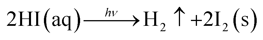
| CH3NH3I(aq) → CH3NH2(aq) + HI(aq) | (2) |
| 4HI(aq) + O2 → 2I2(s) + 2H2O | (3) |
 | (4) |
Ultraviolet light can also cause the degradation of MAPbI3 perovskite. For example, the commonly used TiO2 electron transport layer for these PSCs is susceptible to UV-induced degradation. According to the international standards for climate chamber tests (IEC 61646), solar cells need to maintain long-term stability at 85 °C (=358.15 K).13 The thermal energy at 85 °C corresponds to 0.093 eV, which is very close to the absolute value of formation energy of MAPbI3 (0.11–0.14 eV) obtained from density functional theory (DFT). This indicates that MAPbI3 is intrinsically unstable when continuously exposed to high temperature, which can cause thermal stress.14–23 Its temperature-induced decomposition can take place as follows
| CH3NH3PbI3 → CH3NH2↑ + HI↑ + PbI2(s) exceeding 100 °C | (5) |
In order to improve the chemical stability of MAPbI3-based PSCs against moisture and temperature, researchers have proposed exchanging the MA+ organic cation with another component at the A position. For example, FAPbI3 has been shown to be more thermally stable than MAPbI3 due to its larger tolerance factor. However, FAPbI3 undergoes a phase transition from the black triangle perovskite α-FAPbI3 phase to the yellow hexagonal δ-FAPbI3 phase in the presence of moisture.18,24 Considering the instability of organic cations (MA+ and FA+), researchers believe that the utilization of inorganic cations (Cs+) instead of organic cations can improve the stability of perovskite materials. It should be noted that the trend on the claimed stability of PSCs by changing MA+ to FA+ and then Cs+ has actually shown that, unfortunately, this is not a final solution for the above-mentioned challenges.
Nevertheless, due to their lack of structural stability over thousands of hours, these devices are unappealing for commercial applications, regardless of the developments in device performance. Furthermore, there is currently an intense debate on the use of lead in PSCs, which is believed to be the key component for most perovskites for effective PV.25–27 Though it is for sure that the lead causes toxic problems during device manufacture, deployment, and disposal. In contrast to lead acid batteries, which are composed of (PbSO4 and PbO) highly water-insoluble compounds, MAPbI3 perovskite is easily decomposed into PbI2 with a solubility of 4.4 × 10⁻⁹ in H2O at room temperature.28 For typical MAPbI3 perovskite solar cells, PbI2, hydroiodic acid (HI) and methylamine produced by the decomposition of perovskite may have adverse effects on the environment.29 According to the World Health Organization (WHO), the 50% lethal dose of lead [LD50(Pb)] is less than 5 mg kg−1 of body weight. Since the WHO has stipulated that the highest blood lead level is 5 mg L−1 in children, it is difficult for Pb-based perovskites to pass environmental standards for PV systems.28–31 Hence, the toxicity of lead-based perovskites has become another obvious problem due to the possibility of lead leaching into the environment.
Thus, the key issues of poor device stability associated with intrinsic material instability and toxicity due to water-soluble Pb2+ need to be addressed before large-scale commercialization of perovskite.26,32–34 Herein, two approaches may be effective to address the above-mentioned challenges in the future: suitable encapsulation and new inorganic lead-free perovskite materials. We believe the latter can be an effective strategy from a scientific point of view after evaluating the strategy from the First Solar CdS cells. Therefore, after about ten years of thorough investigation into this type of material, it is essential for scientists to question whether the elimination of organic–inorganic hybrid halide lead perovskites (especially MAPbI3) from PV application is necessary or not. To date, several groups in this research community have vaguely proven their solution to this problem without any official statement. Thus, it is crucial to test alternatives to achieve similar optical and photovoltaic performances for the commercialization of PSCs. Several research groups have begun to replace lead with other elements and replace organic cations with inorganic cations to form suitable new non-toxic and stable perovskite materials (Fig. 2), which may be a long journey before the final commercialization of PSCs.7,35–39 Therefore, this review focuses on the research progress on inorganic lead-free perovskites and their application in photovoltaics in recent years, with the aim to clarify the development of the existing problems.
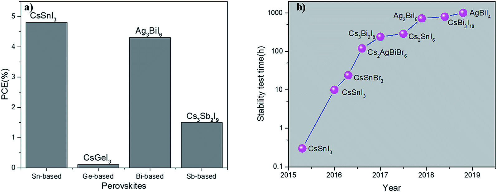 | ||
| Fig. 2 (a) Highest PCE of devices based on different inorganic lead-free perovskite materials reported to date (classified by element). (b) Stability test time evolution of inorganic lead-free perovskites. | ||
2. Perovskite formation and structural consideration
Perovskite compounds are classified into inorganic oxide perovskites, alkali metal halide perovskites, and organic metal halide perovskites. They are represented by the structural formula ABX3, where B is a metal cation and X is an anion composed of oxides or halides. The B and X ions form the BX6 octahedra with B in the center and X in the corner. By connecting the corners, the BX6 octahedra extend to form a three-dimensional structure (Fig. 3).18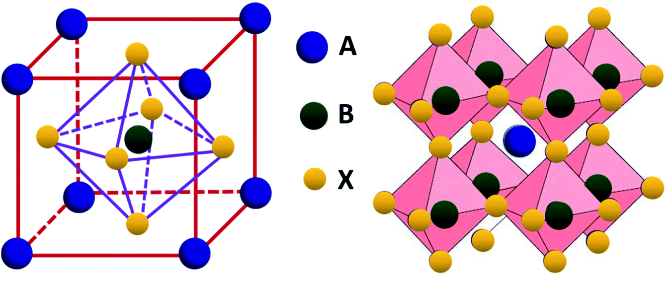 | ||
| Fig. 3 Structure of perovskites with ABX3 formula. | ||
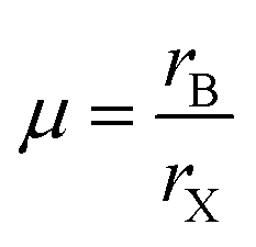
The formation of metal halide perovskite depends on three factors: (1) the charge neutrality between the anions and cations, (2) the stability of the BX6 octahedron predicted by the octahedral factor μ, and (3) the ionic radii of A, B and X are in accordance with the requirements of the Goldschmidt tolerance factor t.9 The octahedral factor μ, which is the ratio of the radius of the B-site cation (rB) and the halide counter ion (rX), can be used to estimate the thermal stability of the BX6 octahedra (eqn (6)). The binding of the B-site cation is determined by the ion size limitations defined by the X6 octahedra. For a value of μ between 0.442 and 0.895, the metal halide perovskite has been found to be stable.
 | (6) |
The Goldschmidt tolerance factor t is calculated to apply the ionic radii of the involved A, B and X ions (rA, rB and rX) according to eqn (7).13 It can be used to evaluate whether different types of A, B and X ions can form the perovskite structure.
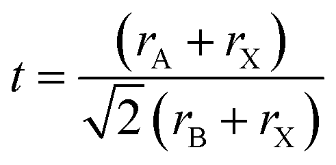 | (7) |
Based on the limitation of ion sizes for the cations and anions involved, the stability and formability of the ABX3 perovskite structure can be determined.40 The tolerance coefficient is empirically found to be 0.8 ≤ t ≤ 1.0. For example, a tolerance coefficient of 1.0 indicates the formation of an ideal ABX3-type perovskite having a cubic crystal structure. If the tolerance coefficient is between 0.9 and 1.0, the perovskite will form a cubic crystal structure. In the case of a t between 0.80 and 0.89, a distorted perovskite structure with an orthorhombic, tetragonal, or rhombohedral crystal structure is most likely to be formed (Fig. 4). Whereas, if the value of t is less than 0.8, then the A cation is too small to form a perovskite structure, and will form an alternative structure such as ilmenite-type FeTiO3. Also for a t greater than 1, the A cation is too large to form a perovskite structure, where a hexagonal structure will be formed instead of layers that, which includes face-sharing octahedra.9,41–45
 | ||
| Fig. 4 Correlation between the crystal structure of perovskite and value of tolerance factor t. | ||
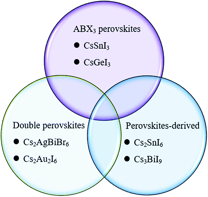
The concept of the Goldschmidt tolerance factor works reasonably with the organic–inorganic metal halide perovskite materials. Furthermore, many researchers have used this parameter to determine whether a combination of several ions can form a stable perovskite structure. In addition, this is also the basis for assessing the feasibility of homovalent or heterovalent Pb substitution in metal lead-based perovskites, as well as the replacement of the A and X sites.27,46 Therefore, the Goldschmidt substitution rule can be used to predict novel inorganic lead-free perovskite materials. According to the crystal structure of inorganic lead-free perovskites currently being studied, we classify inorganic lead-free perovskite materials into three categories: ABX3 perovskite, A2B1+B3+X6 double perovskite and perovskite-derived materials (Fig. 5). This review will also elaborate on the research progress of various inorganic lead-free perovskite solar cells from these three categories, and the future solutions to existing problems.
 | ||
| Fig. 5 Classification of inorganic lead-free perovskites for PV application. | ||
3. ABX3 perovskites
3.1 CsSnI3 perovskite material
Sn and Pb are in the same main family and have similar electronic arrangements. Kanatzidis et al. first synthesized Sn–Pb mixed doped perovskite solar cells and optimized the band gap width of the material by changing the ratio of Sn and Pb.47 Their study showed that Sn is a complete potential replacement for Pb as the light absorbing the material. Subsequently, further investigations were conducted using Sn as a substitute for Pb in perovskite solar cells, where CsSnI3 is a distinctive perovskite material.48,49 In fact, CsSnI3 is not a brand-new material since an early study on the structural information of CsSnI3 compounds in powder for was initially reported by Scaife et al. in 1974. Ten years later, Mauersberger and Huber synthesized a yellow needle-like CsSnI3 crystallite, and its crystal structure was independently identified.50 Additional information was even provided before Yamada et al. discovered another polymorph of this compound in 1991. This polymorph was named black CsSnI3 due to its glossy black color.50 CsSnI3 is a unique phase-change material that exhibits two polymorphs at room temperature: one has a one-dimensional yellow double-chain structure (Y-CsSnI3) and the other one a three-dimensional black perovskite structure (B-γ-CsSnI3) (Fig. 6).51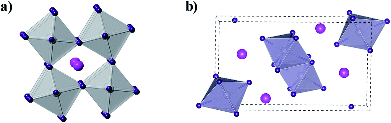 | ||
| Fig. 6 (a) Crystal structure of B-γ-CsSnI3. B(b) Crystal structure of Y-CsSnI3. In these two images, the magenta spheres represent the Cs atoms, the purple spheres represent the I atoms, and the gray spheres represent the Sn atoms. | ||
The B-γ-CsSnI3 perovskite has a photoelectric response, while the Y-CsSnI3 perovskite does not. Therefore, most studies have been generally focused on the application of B-γ-CsSnI3 perovskite. B-γ-CsSnI3 possesses a band gap of 1.3 eV with a corresponding spectral response extending to 950 nm and low exciton binding energy (10–20 meV). The latter implies that only a small driving force is needed to separate most photo-generated carriers into free carriers.52
These superior properties are particularly fascinating for solar cell application. In 2012, Chen et al. described a Schottky solar cell based on B-γ-CsSnI3, which was fabricated via a vacuum-based technique. The solar cell consisted of a simple structure of indium tin oxide (ITO)/CsSnI3/Au/Ti.53 However, the CsSnI3 material is easily oxidized in air. The first article for this material showed a PCE of only 0.9%. B-γ-CsSnI3 is a p-type direct band gap semiconductor with a carrier concentration of 1017 cm−3 and hole mobility of 585 cm2 V−1 s−1.51 Even though B-γ-CsSnI3 is a semiconductor, it is prone to inherent defects associated with Sn vacancies.51 Thus, it is critical to control the inherent defect concentration to optimize the B-γ-CsSnI3-based device. For instance, Sn-rich growth conditions can tune the hole carrier concentration to a medium level. Conversely, excessive Sn can occupy the I sites and SnI antisite defects, and hence act as recombination centers.52 Briefly, moderate Sn-rich conditions are beneficial to improve the performance of B-γ-CsSnI3-based devices. Accordingly, it is inevitable to reduce the inherent defects caused by Sn vacancies to apply the B-γ-CsSnI3 material in solar cell devices.54 These defects can be effectively suppressed via the method of Sn compensation by adding additional Sn-containing compounds (SnF2, SnI2, and SnCl2). These three compounds can effectively inhibit Sn vacancies in the B-γ-CsSnI3 material. Although SnF2 is more chemically stable than the other two compounds, it easily forms a separate phase in CsSnI3 films.52 SnI2 has the best dispersibility in the CsSnI3 precursor solution, but the corresponding device stability is low.55 Compared with the other compounds (SnF2 and SnI2), SnCl2 can significantly improve the stability of CsSnI3 devices.56
3.2 CsSnI3−xBrx-based perovskite solar cells
Although CsSnI3 PSCs have high photocurrent, their efficiency is limited by their low VOC. The substitution of Br for I can increase the band gap of the perovskite material and hence improve the device VOC.60 For instance, by modulating the Br content, the band gaps for CsSnI3, CsSnI2Br, CsSnIBr2, and CsSnBr3 were determined to be 1.27 eV, 1.37 eV, 1.65 eV and 1.75 eV, respectively. The addition of Br also increased the device VOC.60 The VOC improvement is ascribed to the reduced background of the carrier density by several orders of magnitude relative to CsSnI3 and increased charge recombination resistance when I is gradually replaced by Br. However, this increase in VOC was obtained at the expense of the photocurrent. Thus, the primary task of further optimizing the device performance using this type of material is to increase the photocurrent. It was reported that the incorporation of Br in the organic–inorganic halide perovskite (MAPbI3) improved the stability of the device; whereas, the incorporation of Br in the CsSnI3 perovskite material had a minor effect on its stability.60 The chemical instability of CsSnI3−xBrx is due to the tendency of Sn2+ to be oxidized to Sn4+. Thus, suppressing Sn vacancies and reducing the formation of Sn4+ are necessary to improve the device performance. By adding a reductive additive, the precursor can be effectively stabilized while reducing the Sn vacancy concentration and also suppressing charge recombination.61 Similarly to the process of preparing CsSnIBr2 films, adding hypophosphorous acid (HPA) can inhibit the formation of Sn vacancies. HPA possesses a P–O bond, which can strongly coordinate with Sn2+ to stabilize CsSnIBr2 compounds. Furthermore, HPA is a reducing agent, which prevents the oxidation of Sn2+.61 The device demonstrated an improved PCE when the CsSnIBr2 solution with HPA was embedded in the TiO2/Al2O3/C structure, which enhanced the device performance with a VOC of 0.31 V, JSC of 17.4 mA cm−2, FF of 0.56 and PCE of 3.2%. The efficiency of the device with HPA was twice of that without HPA. More importantly, the prepared CsSnIBr2 PSCs exhibited stable device performances for a period of 77 days under atmospheric conditions. When tested at 473 K for 9 h, the device still retained 98% of its initial value, indicating that the device has great thermal stability.61 Gupta et al. preheated the CsSnBr3 precursor solution and substrate at 75 °C and 100 °C, respectively, to produce a high-quality film via a one-step method. The optimal CsSnBr3 PSCs exhibited a PCE of 2.1%, with a JSC of 9 mA cm−2, VOC of 0.41 V, and FF of 58%.623.3 ASnX3 with varying inorganic cations at the A site
The VOC of CsSnI3-based devices is essentially limited by the small ionization potential (IP, approximately 4.9 eV) of the CsSnI3 material, which is only half that of Pb-based perovskite.63 Substitution of Br with I in the CsSnI3 perovskite material can increase its IP and band gap, resulting in an increase in the device VOC. By replacing the Cs cation at the A site with the smaller-sized Rb cation to form Cs1−xRbxSnI3,64 the IP of the material increased to 5.45 eV.63 It was found that the Cs0.8Rb0.2SnI3 PSCs exhibited the best device efficiency of 2.64%. For a low substitution level (x = 0.2), the VOC of the Cs0.8Rb0.2SnI3 PSCs (0.48 V) increased by 120 meV relative to that of pure CsSnI3 (0.36 V), which generally resulted in an increased IP for the perovskite material with the incorporation of Rb. It is worth noting that the band gap of Cs0.8Rb0.2SnI3 (1.33 eV) was only increased by 30 meV relative to that of pure CsSnI3, which means the small amount of Rb substitution did not substantially reduce the wavelength range of light absorption. However, a further increase in the Rb content (x > 0.5) can easily cause SnI6 octahedral lattice distortion and strain, which lead to a decrease in stability.63 The band gap distribution obtained with first-principles DFT calculations over approximately 260 species of inorganic lead-free perovskites further suggests that cubic-KSnCl3 and cubic-RbSnCl3 with ideal band gaps (1.24–1.44 eV) may be potential replacements for Pb-based perovskites.65 Thus, it is worth exploring the photoelectric properties of both materials in the future.3.4 Ge-based perovskite
Lead (Pb) can be replaced by germanium (Ge), for instance, to avoid toxicity and incorporate cesium to strengthen the stability. Ge, which is from the IVA family, is widely used as a dopant to create tailored semiconductor properties by mixing with proper amounts of other elements.66 Compared to Sn and Pb, Ge has a stronger tendency to form sp3 hybrids and let both s and p electrons join in the bonding. When incorporated into perovskites, there is a strong tendency for Ge to move off-center along the diagonal in its octahedral surroundings, resulting in a stronger bonding to three of its halogen neighbors and causes intrinsic stability in perovskites.67 Experimentally, Ge-based halide perovskites with stable rhombohedral crystal structures have been synthesized, which do not show any phase changes in the working temperature range of the device. These compounds are stable up to 150 °C. It is worth mentioning that Ge-based perovskites are a natural extension of the ABX3 family of materials, which still preserve the same basic band structures and suitable band gaps for solar cells. The band gaps of different halide elements (Cl, Br, and I), CsGeCl3, CsGeBr3, and CsGeI3 were calculated to be 3.67 eV, 2.32 eV and 1.53 eV, respectively.66 Therefore, CsGeI3 is more appealing to researchers than the other two. CsGeI3 has a three-dimensional (3D) perovskite structure accompanied by small rhombohedral distortion. Similar to CsSnI3, CsGeI3 is also easily oxidized to present a yellow phase in air. Compared with their Pb-based counterparts, tin and germanium-based perovskite compounds have stronger anti-bonding properties near the valence band maximum (VBM) due to their active Sn 5s lone pair and Ge 4s lone pair. This results in the sudden formation of holes at the VBM of the perovskite material, and as a consequence, brings the oxidization of Sn2+/Ge2+ to Sn4+/Ge4+. Calculations on defect density have showed that CsGeI3 is a p-type semiconductor,66 which suggests that its hole density can be tuned by adjusting the chemical potential of its constituent elements. For instance, CsGeI3 grown under Ge-rich conditions is a semiconductor material with good conductivity and low hole density. Theoretically, this material can be used as a light absorbing material for solar cell application. However, due to its strong short-range potential such as Ge–Ge covalent bonds, the I− defect in CsGeI3 acts as a deeper electron defect than that in CsSnI3 and MAPbI3, which significantly confines electron migration and thus affects the open circuit voltage of solar cells.66 Krishnamoorthy et al. selected DMF as a precursor solvent and used TiO2 and spiro-MeOTAD as ETL and HTL, and initially reported solar cells based on CsGeI3 material. The solar cell had a low VOC of 74 mV and PCE of only 0.11%.67 The reason for the low performance of the device was mainly due to the poor quality of the perovskite film and the poor air stability of the perovskite material, where Ge2+ is oxidized to Ge4+ during film formation and device fabrication. Thus, the poor air stability of CsGeI3 restricted the performance of the device.68 Therefore, increasing the air stability of CsGeI3 remains a challenge in the field of optoelectronics. Mixing tin with germanium to produce new perovskite materials can be a feasible strategy. DFT calculation has revealed that RbSn0.5Ge0.5I3 materials possess desirable band gaps (0.9–1.6 eV) with great light absorption, high carrier mobility, and better water, and thermal stability than organic–inorganic lead-based halide perovskites. Thus, this new inorganic lead-free perovskite material may provide a favorable direction for the development of Sn-based and Ge-based perovskite devices.69A summary of the optical data and structures based on tin, germanium halide perovskites and their performances as absorbing materials in PV devices are given in Table 1.
| Materials | E g (eV) | PL (nm) | Crystal structure | HTL | ETL | PCE/% | Ref. |
|---|---|---|---|---|---|---|---|
| CsSnI3 with SnF2 | 1.27 | 976 | Orthorhombic | Spiro-OMeTAD | TiO2 | 2.02 | 54 |
| CsSnI3 with SnI2 | CuI | Fullerene | 2.78 | 57 | |||
| CsSnI3 with SnI2 | PTAA | TiO2 | 4.81 | 55 | |||
| CsSnI3 with SnCl2 | PCBM | 3.56 | 58 | ||||
| CsSnI3 | NiO | PCBM | 3.31 | 59 | |||
| CsSnI2Br | 1.37 | 905 | Cubic | Spiro-OMeTAD | TiO2 | 1.67 | 60 |
| CsSnIBr2 | 1.65 | 771 | Cubic | TiO2 | 3.2 | 61 | |
| CsSnBr3 | 1.75 | 709 | Cubic | Spiro-OMeTAD | TiO2 | 2.1 | 62 |
| CsGeI3 | 1.53 | 810 | Rhombohedral | Spiro-OMeTAD | TiO2 | 0.11 | 67 |
4. Double perovskite structured materials
4.1 Perovskites with the A2B1+B3+X6 formula
The double perovskite structure A2B1+B3+X6 refers to the simultaneous replacement of the A and B positions by different elements, and in this manner a double perovskite material is alternately arranged by different octahedral structures (Fig. 7).70 Most double perovskite materials are more stable and environmentally friendly than the conventional organic–inorganic hybrid lead halide ABX3 perovskite materials. For instance, the decomposition energies of Cs2AgBiCl6 and Cs2AgBiBr6 are 0.57 eV and 0.38 eV, respectively, which are higher than that of MAPbI3 (0.11–0.14 eV).71 This indicates that these double perovskite materials are more stable than conventional organic–inorganic hybrid lead halide ABX3 perovskite materials. The Sn-based and Ge-based perovskite materials, which are homovalent substituted for Pb cations, severely restrain the in-depth development of materials due to their poor air stability as discussed above. This situation can be improved by forming new inorganic lead-free perovskite materials via the heterovalent substitution of Pb.70 To initiate the heterovalent substitution of the Pb cation and maintain the material charge conserved, the B site must be occupied by a monovalent cation and a trivalent cation. Bi3+ has the same extra-core electron cloud configuration (6s26p0) as Pb2+, which holds potential for the replacement. The appropriate size of Ag+ can be used to maintain material charge conservation and form an effective double perovskite structure due to tolerance factor limitations. The synthesized cubic Fm![[3 with combining macron]](https://www.rsc.org/images/entities/char_0033_0304.gif) m double perovskite Cs2AgBiBr6 exhibited a basic photoluminescence (PL) lifetime of about 660 ns at room temperature.70 This long carrier lifetime indicates the scientific importance for further exploration in the field of optoelectronics. This indirect band semiconductor with an optical band gap of 1.95 eV has significantly higher thermal and moisture stability than MAPbI3. Furthermore, the analogues of Cs2AgBiBr6 and Cs2AgBiCl6 have been successfully synthesized, showing an indirect band gap of 2.19 eV and 2.77 eV, respectively.72 Although the band gap of Cs2AgBiI6 is lower than the former two materials, theoretical calculations specify that Cs2AgBiI6 is thermodynamically unstable. The calculated decomposition energy of Cs2AgBiI6 is −0.41 eV, which means that Cs2AgBiI6 spontaneously decomposes.71
m double perovskite Cs2AgBiBr6 exhibited a basic photoluminescence (PL) lifetime of about 660 ns at room temperature.70 This long carrier lifetime indicates the scientific importance for further exploration in the field of optoelectronics. This indirect band semiconductor with an optical band gap of 1.95 eV has significantly higher thermal and moisture stability than MAPbI3. Furthermore, the analogues of Cs2AgBiBr6 and Cs2AgBiCl6 have been successfully synthesized, showing an indirect band gap of 2.19 eV and 2.77 eV, respectively.72 Although the band gap of Cs2AgBiI6 is lower than the former two materials, theoretical calculations specify that Cs2AgBiI6 is thermodynamically unstable. The calculated decomposition energy of Cs2AgBiI6 is −0.41 eV, which means that Cs2AgBiI6 spontaneously decomposes.71
 | ||
| Fig. 7 Crystal structure of double perovskites. The magenta spheres represent Cs atoms, red spheres represent trivalent metal atoms (Bi and Sb atoms), blue spheres represent a monovalent metal atom (Ag and Cu atoms), and green spheres represent a halogen atom (Cl and Br atom). | ||
Besides understanding their optoelectronic properties, the successful application of these materials in solar cells can be attractive to common readers. The first device using Cs2AgBiBr6 materials was reported by Wu et al.73 Cs2AgBiBr6 powder was dissolved in DMSO solvent to prepare a perovskite film by spin-coating and annealing at different temperatures. It was found that the traditional thermal annealing method caused the Cs2AgBiBr6 film to have poor coverage, and the corresponding devices showed a low PCE (<0.1%). Subsequently, a low pressure-assisted (LPA) method was adopted to prepare a dense and high coverage Cs2AgBiBr6 film. The device displayed a PCE of 1.44%, VOC of 1.04 V, JSC of 1.78 mA cm−2 and FF of 0.78.73 However, the current of the Cs2AgBiBr6 device was lower than that of Pb-based perovskite, and thus, further increasing the current is the key to optimizing device efficiency. Gao et al. employed the anti-solvent strategy to prepare a Cs2AgBiBr6 film. The use of isopropanol (IPA) as an anti-solvent promoted grain nucleation and rapid crystallization to obtain a smooth and uniform Cs2AgBiBr6 film. The best device exhibited a PCE of 2.23%, VOC of 1.01 V, JSC of 3.19 mA cm−2, and FF of 69.2%. The reason for the low efficiency may be due to the limited thickness of the Cs2AgBiBr6 film (only 250 nm), which correlated with low solubility in DMSO (only 0.4 M), thus restraining the photocurrent. Therefore, Greul et al. directly dissolved AgBr, CsBr and BiBr3 powder in DMSO solvent to obtain a precursor solution having a maximum solubility of 0.6 M.74 The device performance was further improved to a PCE of 2.5% with a current of 3.6 mA cm−2via two different heating steps for the preparation of the Cs2AgBiBr6 film, in which the hot precursor solution (75 °C) was spin-coated onto a pre-warmed substrate followed by heat treatment at 285 °C for 5 minutes to effectively improve film coverage. Although Cs2AgBiBr6 PSCs exhibit extremely high stability, their device efficiency should be enhanced to meet market demand.
4.2 Band gap engineering
Double perovskite materials such as Cs2AgBiBr6 and Cs2AgBiCl6 are indirect semiconductors with large band gaps over 2.0 eV. In addition, the exciton binding energy of these materials (over 200 meV) is much higher than that of MAPbI3 (25 meV).73 These unfavorable factors constrain the further development of device performance. As a result, the band gap engineering of these materials and the search for new double perovskite materials have gained attention. For example, the band gap of Cs2AgBiBr6 can be tuned by a small amount of substitution of Sb and In for Bi.75 The different atomic structures of Sb and In can induce the change in band gap of these perovskite material. The addition of In increases the band gap of Cs2AgBiBr6, while the addition of Sb decreases the band gap. Cs2Ag(Bi0.625Sb0.375)Br6 possessed a suitable band gap value of 1.86 eV.75 Moreover, partially substituting Ag with Cu in Cs2BiAgBr6 can efficiently reduce the band gap of Cs2BiAgBr6. Cs2BiAg1−xCuxCl6 possessed a band gap of 1.6–1.9 eV with good stability.33 In addition to the partial substitution of Ag and Bi elements to modulate the band gap of the Cs2AgBiBr6 material, a direct band gap of 1.57 eV was obtained for Cs2AgBiBr6 by adding 0.075% Tl to modify the band edge of Cs2AgBiBr6.75 However, interestingly, to date, there are no reports on the use of these materials for solar cell application.Likewise, the deployment of new double perovskite materials has become the focus of researchers. Recently, the photoelectric properties of Cs2Au2I6 have been under comprehensive investigation. DFT calculation has shown that the charge disproportionation on Au makes the two Au atoms have a valence of +1 and +3, which results in Cs2Au2I6 being a double perovskite material.76 This raises a different type of material from the previous ABX3-structured perovskites. By first-principles calculation, the band gap of Cs2Au2I6 was estimated to be 1.31 eV, which is close to the optimal value for PV materials suggested by the Shockley–Queisser theory. In addition, unlike the previously discussed double perovskite materials, Cs2Au2I6 is a direct band gap semiconductor. Debbichi et al. optically simulated the suitability of Cs2Au2I6 in a PV device with the structure of ITO/TiO2/perovskite layer/spiro-OMeTAD/Au.77 The results specified that the Cs2Au2I6-based device can deliver a PCE of 18.2% with JSC of 25 mA cm−2 even with a perovskite layer of around 50 nm. Theoretical studies have shown that the highest JSC of Cs2Au2I6 devices can even exceed 30 mA cm−2, thus exceeding a PCE of 20%. This is comparable to the most popular Pb-based PSCs. In conclusion, Cs2Au2I6-based PSCs hold the potential for a big event in the development of perovskite.
4.3 AA′B2X6 perovskite
In addition to the common replacement of Cs+ at the A position of most double perovskite materials, co-doping of Rb+ and Cs+ is captivating due to their similar chemical activity.78 In 2016, Gou et al. obtained the (CsRb)2Sn2I6 double perovskite structure material by doping Rb in CsSnI3 to allow Rb and Cs to occupy the A position in the perovskite material. Although the bandgap of this material (Eg = 1.58 eV) is larger than the band gap of CsSnI3, studies have shown that the carrier effective mass of this double perovskite material is comparable to that of the CsSnI3 material. More importantly, the (CsRb)Sn2I6 material has ferroelectricity and can promote the separation of photogenerated carriers due to the coupling of the rotation and polarization misalignment of the [SnI6] octahedron, forming a new type of ferroelectric PV with potentially enhanced PCE.785. Perovskite-derived materials
5.1 A2BX6 formula
With detailed studies of perovskite materials widely used in optoelectronic devices, a series of similar materials to perovskite have slowly been revealed. In addition to the above-mentioned ABX3 and A2B1+B3+X6 inorganic perovskite materials, inorganic lead-free perovskite-derived materials have acquired increasing attention in the past two years.Cs2SnI6 is a lead-free perovskite-derived material with Sn defects.79 Cs2SnI6 films can be directly obtained via a two-step deposition method. The material has a band gap of only 1.6 eV and carrier density of 1016 cm−3, which was originally used as an HTL for dye-sensitized solar cell devices.80 B-γ-CsSnI3 films prepared via the two-step method can be spontaneously oxidized to an air-stable Cs2SnI6 film in the external environment.81 Cs2SnI6 is a defect variant of the CsSnI3 perovskite structure, and half of the octahedral Sn atoms are missing, resulting in isolated [SnI6]2− octahedra (Fig. 8). Due to the existence of Sn4+, the stability of Cs2SnI6 is significantly higher than that of CsSnI3. Furthermore, Cs2SnI6 has a direct band gap of 1.48 eV and a high absorption coefficient (over 105 cm−1), which is suitable for use as a light absorber.79 However, the first PSCs based on Cs2SnI6 materials in combination with TiO2 and P3HT as ETL and HTL showed a VOC and JSC of 0.51 V and 5.41 mA cm−2, respectively, achieving a PCE of up to 0.96%.81 Although this efficiency was lower than that of lead-based perovskites, the device cell was stable in an air environment for more than one month. Cs2SnI6 only decomposes at a temperature of 250 °C; therefore, in principle, this material possesses superior stability compared with the traditional perovskite materials. The many defects (iodine vacancy and tin interstitial) in Cs2SnI6 and its low electron mobility (2.9 cm2 V−1 s−1), as well as its large effective mass of holes, result in low PCE for devices with Cs2SnI6 as the light absorbing layer.79 The performance can be further improved by replacing Br with I in Cs2SnI6. A band gap tunable Cs2SnI6−xBrx film (1.3–2.9 eV) was synthesized via a two-step method,82 and the best device based on the Cs2SnI4Br2 (x = 2) material exhibited a PCE of 2.1%. This was because the intrinsically deep defects of Cs2SnI6 narrowed the device performance.
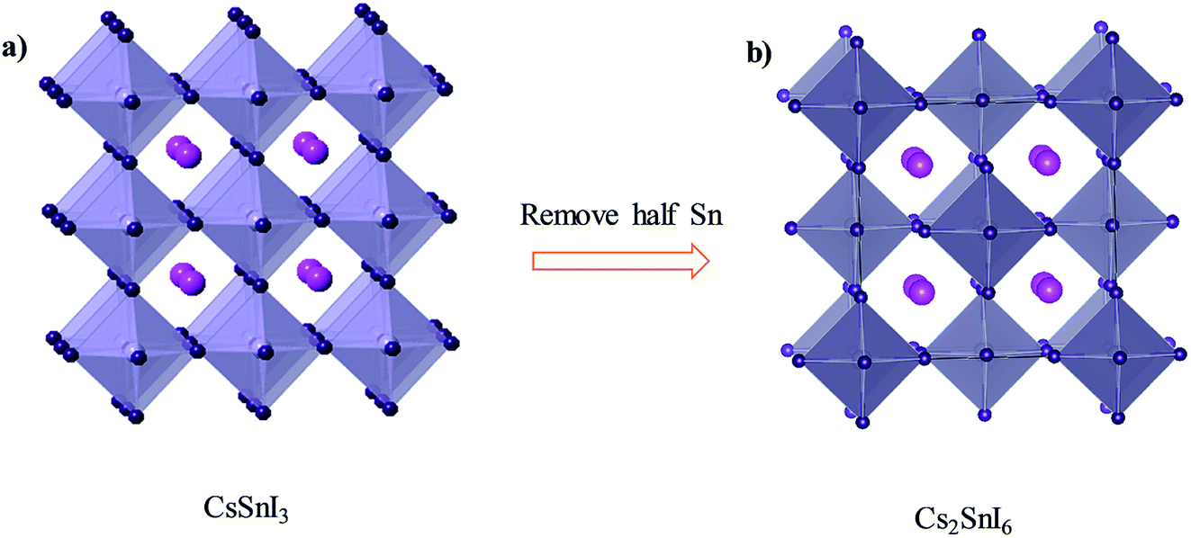 | ||
| Fig. 8 (a) Crystal structure of CsSnI3. (b) Crystal structure of Cs2SnI6. Consulting from ref. 79. | ||
Replacing the Sn4+ cation with transition metal cations can result in new perovskite materials, such as Cs2PdBr6.83 The Cs2PdBr6 compound exhibits a band gap of 1.6 eV and long-lived photoluminescence. A simple “sandwich structure” device with ITO/Cs2PdBr6/Ag was fabricated to evaluate whether Cs2PdBr6 had optoelectronic properties. The photo-response of the device indicated that this material may be suitable for use in solar cells. A phase change and chemical decomposition were not observed when the Cs2PdBr6 crystal was placed in water for 10 minutes, indicating that this material has greater stability compared to lead-based perovskite materials. Similarly, the non-toxic Ti element can replace Sn to obtain novel perovskite materials such as Cs2TiIxBr6−x.84 Cs2TiIxBr6−x materials were synthesized via the melt-crystallization method, and subsequent experimental measurement and theoretical computations showed that these materials had band gaps in the range of 1.0 eV to 1.8 eV. Moreover, the Cs2TiIxBr6−x materials have benign defect properties, excellent light absorption, and high stability.84 Thus, these materials are worth examining in the future. Chen et al. first reported Cs2TiBr6 PSCs and demonstrated experimentally the photoelectric effect of Ti-based perovskite materials. A Cs2TiBr6 film was prepared via a low-temperature vapor method, a uniform CsBr film was first deposited on the substrate by thermal evaporation, and then the CsBr film was annealed in a TiBr4 vapor atmosphere at 200 °C. The Cs2TiBr6 film presented a band gap of 1.8 eV, electron and hole diffusion length exceeding 100 nm, and excellent environmental stability. The device structure with FTO/TiO2/C60/Cs2TiBr6/P3HT/Au was adopted to evaluate the PV performance of the Cs2TiBr6 material. The C60 layer was added to facilitate electron transfer from the Cs2TiBr6 layer to the TiO2 layer and modify the CsBr microstructure, yielding a uniform CsBr film. The device delivered a PCE of 3.3% with a JSC of 5.69 mA cm−2 and VOC of 1.02 V.
5.2 A3B2X9 formula
A3B2X9 is the structural formula of another representative class of perovskite-derived materials. Cs is usually used to occupy the position of A, whereas Bi occupies the position of B, which gives different crystal structures. Since Bi3+ and Pb2+ are in different valence states, it is impossible to directly replace Pb in perovskites to form 3D the ABX3 structure.85 Therefore, the structure of Bi-based perovskite materials is different from that of 3D Pb-based perovskites, which have huge structural diversity of 0D, 1D, 2D, and 3D structures. The Cs3Bi2I9 material belongs to the 0D structure and consists of bioctahedral (Bi2I9)3− clusters surrounded by Cs+ cations (Fig. 9).86 Park et al. first reported a Cs3Bi2I9 film obtained via a simple solution-processing method. The band gap of the Cs3Bi2I9 material is about 2.1 eV (Table 2). The solar cells constructed with the structure of FTO/m-TiO2/Cs3Bi2I9/spiro-MeOTAD/Ag showed a PCE of 1.09%, with a VOC of 0.85 V and JSC of 2.15 mA cm−2.85 DFT calculations further revealed that Cs3Bi2I9 has a high carrier effective mass, large indirect band gap, and many deep defects.87 However, the devices based on the Cs3Bi2I9 material somehow displayed low PCE in many selected structures.88 This indicates that the Cs3Bi2I9 material may be unsuitable for solar cells applications. Nevertheless, CsBi3I10 films with a low band gap of 1.77 eV were further synthesized via a solution method.89 The comparison of absorption curves revealed that CsBi3I10 had better light absorption than Cs3Bi2I9 with a cutoff edge at 700 nm. Importantly, the layer structured CsBi3I10 can be fabricated into a dense and uniform film. The device with CsBi3I10 as the light absorbing material exhibited a PCE of 0.4%, while the device with Cs3Bi2I9 as the light absorbing material under the same conditions had a PCE of only 0.02%. Impressively, Shin et al. chose low-cost carbon as the electrode to fabricate the device of FTO/c-TiO2/m-TiO2/CsBi3I10/ZrO2/carbon, showing a PCE of 1.51%.90 The device retained its performance when exposed to air for 30 days, indicating its excellent stability.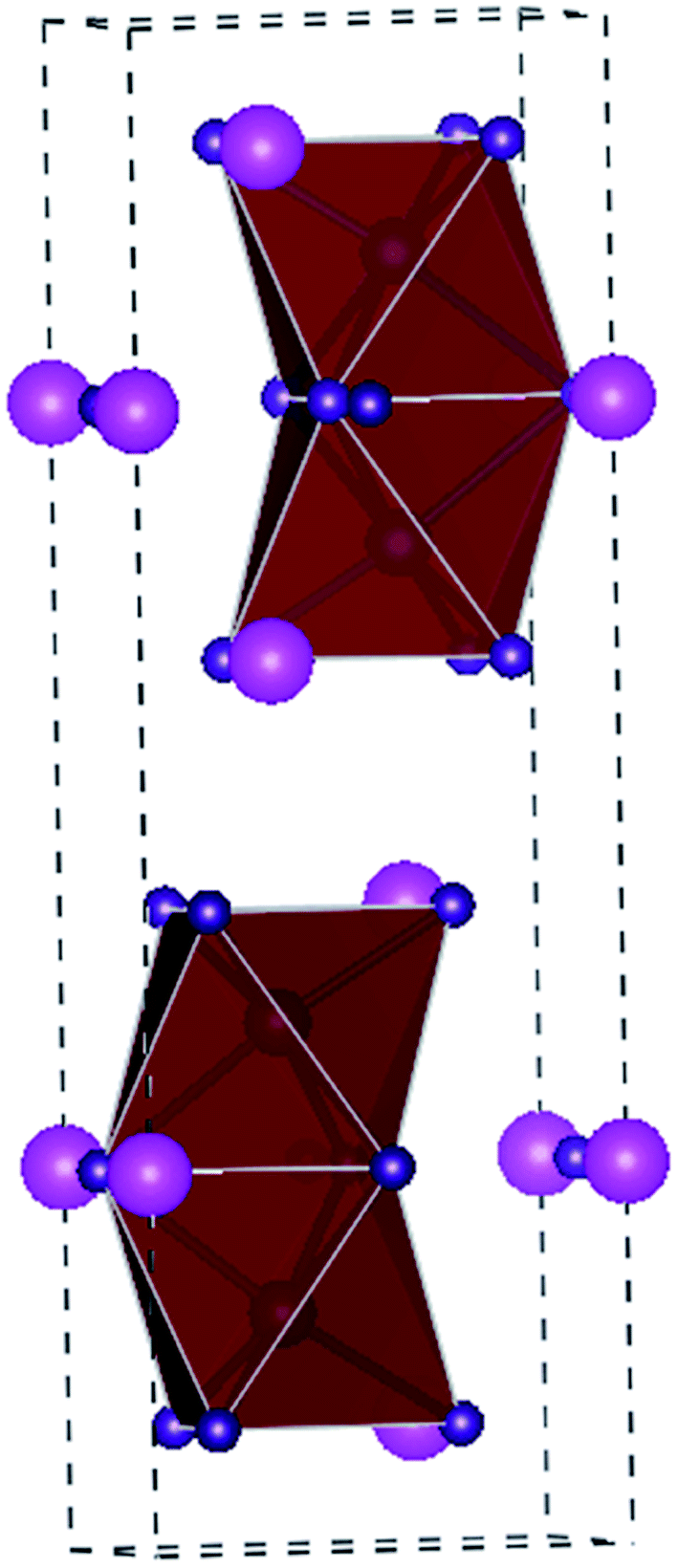 | ||
| Fig. 9 Crystal structure of A3B2I9 perovskites. The magenta spheres represent the Cs atoms, blue spheres represent the trivalent metal atom (Bi, Sb atom), and purple spheres represent the I atom. | ||
| Materials | E g (eV) | HTL | ETL | PCE/% | Ref. |
|---|---|---|---|---|---|
| Cs2SnI6 | 1.48 | P3HT | TiO2 | 0.96 | 81 |
| Cs2SnI5Br | 1.56 | Cs2SnI6 | TiO2 | 1.6 | 82 |
| Cs2SnI4Br2 | 1.58 | Cs2SnI6 | TiO2 | 2.1 | 82 |
| Cs2SnI2Br4 | 1.81 | Cs2SnI6 | TiO2 | 1.08 | 82 |
| Cs2SnIBr5 | 2.36 | Cs2SnI6 | TiO2 | 0.002 | 82 |
| Cs2SnBr6 | 2.85 | Cs2SnI6 | TiO2 | 82 | |
| Cs2PdBr6 | 1.6 | 83 | |||
| Cs2TiBr6 | 1.8 | P3HT | TiO2 | 3.3 | 96 |
| Cs3Bi2I9 | 2.1 | Spiro-MeOTAD | TiO2 | 1.09 | 85 |
| CsBi3I10 | 1.77 | P3HT | TiO2 | 0.4 | 89 |
| CsBi3I10 | TiO2 | 1.51 | 90 | ||
| Cs3Sb2I9 | 2.05 | PEDOT:PSS | PC70BM | 1.5 | 92 |
| AgBi2I7 | 1.87 | P3HT | TiO2 | 1.22 | 93 |
| Ag2BiI5 | 1.85 | P3HT | TiO2 | 2.1 | 94 |
| AgBiI4 | 1.86 | PTAA | TiO2 | 2.1 | 95 |
| Ag3BiI6 | 1.83 | PTAA | TiO2 | 4.3 | 28 |
Sb and Bi have similar electronic configurations and can form A3B2X9 structure perovskite compounds as well.91 Similar to Bi-based perovskites, Sb-based perovskite has the basic structure of A3Sb2X9 with a 0D dimer crystal structure or 2D layered crystal structure. For example, Cs3Sb2I9 with a 2D layered crystal structure is formed at 250 °C, while Cs3Sb2I9 with a 0D dimer crystal structure is formed at 150 °C.92 The layered structure has a direct band gap of 2.05 eV, while it is 2.3 eV for the dimer structured materials. With the structure of ITO/PEDOT:PSS/Cs3Sb2I9/PC70BM/C60/BCP/Al, the devices based on Cs3Sb2I9 with layered and dimer structures achieved PCE of 1.5% and 0.89%, respectively. The difference can be ascribed to the lower band gap and higher carrier mobility of the former.86 This structure has more deep level defects, which can serve as the center of non-radiative recombination, thus disrupting the device performance.91 It is vital to note that even though perovskite-derived materials with the A3B2X9 formula have great potential in the field of optoelectronics, unfortunately, their band gaps are relatively large, and these materials have many defects, which may restrict the further development of device performance based on such materials. In summary, these types of materials need to be examined further, especially their structural regulation.
5.3 AgaBibIa+3b formula
Compared to low-dimensional materials, 3D materials are more conducive to PV applications considering their semiconductor properties. Transition metal monovalent silver and copper cations (Ag+ and Cu+) have been introduced into iodobismuthate materials to form 3D structures.86 For example, a synthetic air-stabilized Ag–Bi–I film was proposed for the fabrication of the AgBi2I7 film. AgI and BiI3 were dissolved in n-butylamine solvent to obtain a precursor solution and the precursor was annealed at 150 °C to remove n-butylamine, which previously was bound to the silver iodide and bismuth iodide complexes.93 The AgBi2I7 film was determined to be a cubic structure with an Eg of 1.87 eV. As a result, the solar cell devices produced a JSC of 3.30 mA cm−2, a VOC of 0.56 V, an FF of 0.67, and a PCE of 1.22%. It was found that the device retained 93% of its PCE upon initial exposure to the external environment after 10 days, indicating the device had great stability.93 A further improvement in PCE to 2.1% was obtained using an Ag2BiI5 film with a hexagonal structure and Eg of 1.85 eV. Photocurrent generation was observed between 350 nm and 700 nm, and the maximum external quantum efficiency of about 45% was obtained.94 AgBiI4 as a lead-free light absorbing material was further synthesized via the solution-based thin film method and assembled in mesoporous solar cell devices.95 A dense and smooth AgBiI4 film was obtained by treatment with an anti-solvent during spin coating and subsequent annealing. AgBiI4 has a low Eg of 1.86 eV and an absorption spectrum in the range of 400 nm to 720 nm, which is suitable for light trapping in thin film solar cells. By using different HTLs (PTAA and P3HT) in the device, better energy alignment between PTAA and AgBiI4 resulted in more efficient hole extraction efficiency in the active material and a higher PCE of 2.1%. The device also exhibited excellent long-term air stability, maintaining 96% of its initial PCE even after 1000 hours in relative humidity of 26%.95 Turkevych et al. studied the structure and optoelectronic properties of a promising family of stable Pb-free photovoltaic halides with the general formula AgaBibIx (x = a + 3b) including nominal compositions of Ag3BiI6, Ag2BiI5, AgBiI4, and AgBi2I7. The Ag–Bi–I ternary group reveals three-dimensional structures of edge-sharing [AgI6] and [BiI6] octahedra.28 The Ag–Bi–I compositions have direct optical band gaps in the range of 1.79–1.83 eV. Though AgI is insoluble in DMSO, the mixture of AgI and BiI3 is readily soluble in hot DMSO at 110 °C due to the formation of [BiI3+x]x− complex ions. Therefore, solar cell devices can be fabricated with the solution-processed method, reaching a PCE of 4.3% with a JSC of 10.7 mA cm−2, VOC of 0.63 V, an FF of 0.64. This indicates that silver-bismuth halide materials have great potential as lead-free light absorbers for PSCs. A summary of the optical data structure and structure based on perovskite-derived materials and also their performances as absorbing materials in PV devices are given in Table 2. It is worth mentioning that there are still a few studies on perovskite-derived materials. Most of the research has focused on the optoelectronic properties of material and there is still a lack of research on the fabrication process and structure optimization for better performance. Although, considering various aspects, these materials can meet the requirements as a light absorbing layer, the current photoelectric conversion efficiency produced from the devices has not exceeded expectation. Therefore, optimizing the components of the device and its interface and also matching the hole transport layer and electron transport layer materials of different energy levels according to different light absorbing materials have become important directions in future research.6. Conclusion and outlooks
The recent progress on the research on perovskite solar cells has been systematically reviewed. It may be a stretch to compare these strategies in PSCs to the “Emperor's New Clothes”. After all, the dictionary definition of strategy is so broad that virtually any declarative sentence that expresses some form of desire qualifies as a strategy. However, in the real world, a true strategy has to have a tangible plan and a clear program to implement that plan. This means making difficult trade-offs and setting clear priorities. However, unfortunately, most of these so-called effective strategies published in top journals, including Science and Nature, based on the selection criterion of ‘THE FIRST’ and/or ‘THE BEST’ have failed in practice and reproduction. Furthermore, most of them did not address any of the major problems in environmental security and national programs created by the existing fundamental debate or the far more serious issues raised on ethics for the future of humans. We note that inorganic lead-free perovskite materials generally have greater light absorption properties, thermal stability, and environmental friendliness compared to lead-containing perovskite materials. The highest PCE achieved for an inorganic lead-free perovskite solar cell was 4.81% for CsSnX3, but with poor air stability. In the case of the double-perovskite inorganic lead-free material, due to the difficulty in preparation of high-quality films, only Cs2AgBiBr6 was successfully used in device fabrication with an efficiency of less than 2%. Perovskite-derived materials such as AgaBibIx have exhibited potential in solar cell application with a PCE of about 4.3%. In addition to Cs and Rb, the use of other cations at the A site of the perovskite material is likely to achieve considerable performance. It is fair that the use of inorganic lead-free perovskite materials as a light-absorbing layer is in its infancy, and their solar cell efficiency cannot be compared to that of traditional organic–inorganic hybrid perovskites yet. This requires further comprehensive and systematic research on structural composition, high-quality film preparation, and development of new inorganic lead-free perovskite materials, electron transport layers and hole transport layers. Composition engineering of this type of material can be the focus of research to further enhance its photoelectric performances. A blend of elements in the A, B, and X sites of the perovskite composition can be plausible in this case. In addition, effective methods have to be developed for the preparation of high quality films, including chemical vapor deposition and dynamic hot-casting techniques. More importantly, solar cell device characterization for most of the new inorganic lead-free materials needs to be fulfilled urgently. Therefore, there is no doubt that novel inorganic lead-free perovskite solar cells still have a lot of space for exploration. Selecting appropriate electron transport layer and hole transport layer materials is beneficial to improve the PCE of solar cells. The commercialization of perovskite solar cells requires extensive research and development of new perovskite materials that are not only very effective in photoelectric conversion but also non-toxic and stable. Thus, in the next few years, more efforts are required for the development of inorganic lead-free perovskite solar cells.Conflicts of interest
There are no conflicts to declare.Acknowledgements
The authors acknowledge financial support from the Natural Science Foundation of China (No. 21673091), the NSFC Major International (Regional) Joint Research Project NSFC-SNSF (No. 51661135023), the Natural Science Foundation of Hubei Province (No. 2015CFA125), the Central Universities of Huazhong University of Science & Technology (2018KFYXKJC034), and the Double first-class research funding of China-EU Institute for Clean and Renewable Energy (3011187029).References
- D. Wang, M. Wright, N. K. Elumalai and A. Uddin, Sol. Energy Mater. Sol. Cells, 2016, 147, 255–275 CrossRef CAS.
- Q. Sun, X. Gong, H. Li, S. Liu, X. Zhao, Y. Shen and M. Wang, Sol. Energy Mater. Sol. Cells, 2018, 185, 111–116 CrossRef CAS.
- M. Green, A. Ho-Baillie and H. Snaith, Nat. Photonics, 2014, 8, 506–514 CrossRef CAS.
- N. Rolston, A. Printz, J. Tracy, H. Weerasinghe, D. Vak, L. Haur, A. Priyadarshi, N. Mathews, D. Slotcavage, M. McGehee, R. Kalan, K. Zielinski, R. Grimm, H. Tsai, W. Nie, A. Mohite, S. Gholipour, M. Saliba, M. Grätzel and R. H. Dauskardt, Adv. Energy Mater., 2018, 8, 1702116 CrossRef.
- H. Li, J. Lu, T. Zhang, Y. Shen and M. Wang, ACS Energy Lett., 2018, 3, 1815–1823 CrossRef CAS.
- X. Zhao and M. Wang, Materials Today Energy, 2018, 7, 208–220 CrossRef.
- J. Huang, Y. Yuan, Y. Shao and Y. Yan, Nat. Rev. Mater., 2017, 2, 17042 CrossRef CAS.
- X. Zhao, L. Tao, H. Li, W. Huang, P. Sun, J. Liu, S. Liu, Q. Sun, Z. Cui, L. Sun, Y. Shen, Y. Yang and M. Wang, Nano Lett., 2018, 18, 2442–2449 CrossRef CAS PubMed.
- Z. Chen, Z. Chen, H. Li, X. Zhao, M. Zhu and M. Wang, Adv. Opt. Mater., 2018, 6, 1800221 CrossRef.
- D. Li, P. Liao, X. Shai, W. Huang, S. Liu, H. Li, Y. Shen and M. Wang, RSC Adv., 2016, 6, 89356–89366 RSC.
- T. Leijtens, G. Eperon, N. Noel, S. Habisreutinger, A. Petrozza and H. Snaith, Adv. Energy Mater., 2015, 5, 1500963 CrossRef.
- X. Xu and M. Wang, Sci. China: Chem., 2016, 60, 396–404 CrossRef.
- T. Leijtens, G. Eperon, N. Noel, S. Habisreutinger, A. Petrozza and H. Snaith, Adv. Energy Mater., 2015, 5, 1500963–1500985 CrossRef.
- N. Aristidou, I. Sanchez-Molina, T. Chotchuangchutchaval, M. Brown, L. Martinez, T. Rath and S. Haque, Angew. Chem., Int. Ed., 2015, 54, 8208–8212 CrossRef CAS PubMed.
- M. Asghar, J. Zhang, H. Wang and P. Lund, Renewable Sustainable Energy Rev., 2017, 77, 131–146 CrossRef CAS.
- T. A. Berhe, W. Su, C. Chen, C. Pan, J. Cheng, H. Chen, M. Tsai, L. Chen, A. Dubale and B. Hwang, Energy Environ. Sci., 2016, 9, 323–356 RSC.
- X. Zhao and N. Park, ACS Photonics, 2015, 2, 1139–1151 CrossRef CAS.
- N. Tiep, Z. Ku and H. Fan, Adv. Energy Mater., 2016, 6, 1501420 CrossRef.
- M. Shahbazi and H. Wang, Sol. Energy, 2016, 123, 74–87 CrossRef CAS.
- Z. Wang, Z. Shi, T. Li, Y. Chen and W. Huang, J. Am. Chem. Soc., 2017, 36, 1190–1212 Search PubMed.
- Q. Fu, X. Tang, B. Huang, T. Hu, L. Tan, L. Chen and Y. Chen, Adv. Sci., 2018, 5, 1700387 CrossRef PubMed.
- B. Li, Y. Li, C. Zheng, D. Gao and W. Huang, RSC Adv., 2016, 6, 38079–38091 RSC.
- B. Salhi, Y. Wudil, M. Hossain, A. Al-Ahmed and F. Al-Sulaiman, Renewable Sustainable Energy Rev., 2018, 90, 210–222 CrossRef CAS.
- M. Wang, Sci. Bull., 2016, 62, 249–255 CrossRef.
- A. Abate, Joule, 2017, 1, 659–664 CrossRef CAS.
- X. Shai, L. Zuo, P. Sun, P. Liao, W. Huang, E. Yao, H. Li, S. Liu, Y. Shen, Y. Yang and M. Wang, Nano Energy, 2017, 36, 213–222 CrossRef CAS.
- X. Shai, J. Wang, P. Sun, W. Huang, P. Liao, F. Cheng, B. Zhu, S. Chang, E. Yao, Y. Shen, L. Miao, Y. Yang and M. Wang, Nano Energy, 2018, 48, 117–127 CrossRef CAS.
- I. Turkevych, S. Kazaoui, E. Ito, T. Urano, K. Yamada, H. Tomiyasu, H. Yamagishi, M. Kondo and S. Aramaki, ChemSusChem, 2017, 10, 3754–3759 CrossRef CAS PubMed.
- A. Babayigit, A. Ethirajan, M. Muller and B. Conings, Nat. Mater., 2016, 15, 247–251 CrossRef CAS PubMed.
- I. Benmessaoud, A. Mahul-Mellier, E. Horvath, B. Maco, M. Spina, H. Lashuel and L. Forro, Toxicol. Res., 2016, 5, 407–419 RSC.
- N. Espinosa, L. Serrano-Luján, A. Urbina and F. Krebs, Sol. Energy Mater. Sol. Cells, 2015, 137, 303–310 CrossRef CAS.
- J. Ball and A. Petrozza, Nat. Energy, 2016, 1, 16149 CrossRef CAS.
- M. Filip, X. Liu, A. Miglio, G. Hautier and F. Giustino, J. Phys. Chem. C, 2017, 122, 158–170 CrossRef.
- X. Zhao, J. Yang, Y. Fu, D. Yang, Q. Xu, L. Yu, S. Wei and L. Zhang, J. Am. Chem. Soc., 2017, 139, 2630–2638 CrossRef CAS PubMed.
- T. Jellicoe, J. Richter, H. Glass, M. Tabachnyk, R. Brady, S. Dutton, A. Rao, R. Friend, D. Credgington, N. Greenham and M. L. Bohm, J. Am. Chem. Soc., 2016, 138, 2941–2944 CrossRef CAS PubMed.
- X. Zhou, J. Jankowska, H. Dong and O. V. Prezhdo, J. Energy Chem., 2017, 26, 21–49 Search PubMed.
- P.-F. Li, Y.-Y. Tang, W.-Q. Liao, H.-Y. Ye, Y. Zhang, D.-W. Fu, Y.-M. You and R.-G. Xiong, NPG Asia Mater., 2017, 9, e342 CrossRef CAS.
- B. Saparov and D. B. Mitzi, Chem. Rev., 2016, 116, 4558–4596 CrossRef CAS PubMed.
- F. Hao, C. Stoumpos, D. Cao, R. Chang and M. Kanatzidis, Nat. Photonics, 2014, 8, 489–494 CrossRef CAS.
- W. Travis, E. Glover, H. Bronstein, D. Scanlon and R. Palgrave, Chem. Sci., 2016, 7, 4548–4556 RSC.
- X. He, Y. Qiu and S. Yang, Adv. Mater., 2017, 29, 1700775 CrossRef.
- W. Zhang, G. Eperon and H. Snaith, Nat. Energy, 2016, 1, 16048 CrossRef CAS.
- M. Saidaminov, O. Mohammed and O. Bakr, ACS Energy Lett., 2017, 2, 889–896 CrossRef CAS.
- M. Petrus, J. Schlipf, C. Li, T. Gujar, N. Giesbrecht, P. Müller-Buschbaum, M. Thelakkat, T. Bein, S. Hüttner and P. Docampo, Adv. Energy Mater., 2017, 7, 1700264 CrossRef.
- M. Green and A. Ho-Baillie, ACS Energy Lett., 2017, 2, 822–830 CrossRef CAS.
- Q. Zhang, F. Hao, J. Li, Y. Zhou, Y. Wei and H. Lin, Sci. Technol. Adv. Mater., 2018, 19, 425–442 CrossRef PubMed.
- J. Im, C. Stoumpos, H. Jin, A. Freeman and M. Kanatzidis, J. Phys. Chem. Lett., 2015, 6, 3503–3509 CrossRef CAS PubMed.
- J. Feng, APL Mater., 2014, 2, 081801 CrossRef.
- G. Lin, Y. Lin, H. Huang, R. Cui, X. Guo, B. Liu, J. Dong, X. Guo and B. Sun, Nano Energy, 2016, 27, 638–646 CrossRef CAS.
- K. Shum, Z. Chen, J. Qureshi, C. Yu, J. Wang, W. Pfenninger, N. Vockic, J. Midgley and J. Kenney, Appl. Phys. Lett., 2010, 96, 221903 CrossRef.
- I. Chung, J. Song, J. Im, J. Androulakis, C. Malliakas, H. Li, A. Freeman, J. Kenney and M. Kanatzidis, J. Am. Chem. Soc., 2012, 134, 8579–8587 CrossRef CAS PubMed.
- M. Konstantakou and T. Stergiopoulos, J. Mater. Chem. A, 2017, 5, 11518–11549 RSC.
- Z. Chen, J. Wang, Y. Ren, C. Yu and K. Shum, Appl. Phys. Lett., 2012, 101, 093901 CrossRef.
- M. Kumar, S. Dharani, W. Leong, P. Boix, R. Prabhakar, T. Baikie, C. Shi, H. Ding, R. Ramesh, M. Asta, M. Graetzel, S. Mhaisalkar and N. Mathews, Adv. Mater., 2014, 26, 7122–7127 CrossRef CAS PubMed.
- T. Song, T. Yokoyama, S. Aramaki and M. Kanatzidis, ACS Energy Lett., 2017, 2, 897–903 CrossRef CAS.
- K. Marshall, M. Walker, R. Walton and R. Hatton, Nat. Energy, 2016, 1, 1–13 Search PubMed.
- K. Marshall, R. Walton and R. Hatton, J. Mater. Chem. A, 2015, 3, 11631–11640 RSC.
- T. Song, T. Yokoyama, C. Stoumpos, J. Logsdon, D. Cao, M. Wasielewski, S. Aramaki and M. Kanatzidis, J. Am. Chem. Soc., 2017, 139, 836–842 CrossRef CAS PubMed.
- N. Wang, Y. Zhou, M. Ju, H. Garces, T. Ding, S. Pang, X. Zeng, N. Padture and X. Sun, Adv. Energy Mater., 2016, 6, 1601130 CrossRef.
- D. Sabba, H. Mulmudi, R. Prabhakar, T. Krishnamoorthy, T. Baikie, P. Boix, S. Mhaisalkar and N. Mathews, J. Phys. Chem. C, 2015, 119, 1763–1767 CrossRef CAS.
- W. Li, J. Li, J. Li, J. Fan, Y. Mai and L. Wang, J. Mater. Chem. A, 2016, 4, 17104–17110 RSC.
- S. Gupta, T. Bendikov, G. Hodes and D. Cahen, ACS Energy Lett., 2016, 1, 1028–1033 CrossRef CAS.
- K. Marshall, S. Tao, M. Walker, D. Cook, J. Lloyd-Hughes, S. Varagnolo, A. Wijesekara, D. Walker, R. I. Walton and R. Hatton, Mater. Chem. Front., 2018, 2, 1515–1522 RSC.
- J. Jiang, C. Onwudinanti, R. Hatton, P. Bobbert and S. Tao, J. Phys. Chem. C, 2018, 122, 17660–17667 CrossRef CAS PubMed.
- X. Mao, L. Sun, T. Wu, T. Chu, W. Deng and K. Han, J. Phys. Chem. C, 2018, 122, 7670–7675 CrossRef CAS.
- W. Ming, H. Shi and M. Du, J. Mater. Chem. A, 2016, 4, 13852–13858 RSC.
- T. Krishnamoorthy, H. Ding, C. Yan, W. Leong, T. Baikie, Z. Zhang, M. Sherburne, S. Li, M. Asta, N. Mathews and S. Mhaisalkar, J. Mater. Chem. A, 2015, 3, 23829–23832 RSC.
- M. Roknuzzaman, K. Ostrikov, H. Wang, A. Du and T. Tesfamichael, Sci. Rep., 2017, 7, 14025 CrossRef PubMed.
- P. Cheng, T. Wu, J. Liu, W. Deng and K. Han, J. Phys. Chem. Lett., 2018, 9, 2518–2522 CrossRef CAS PubMed.
- A. Slavney, T. Hu, A. Lindenberg and H. Karunadasa, J. Am. Chem. Soc., 2016, 138, 2138–2141 CrossRef CAS PubMed.
- C. Savory, A. Walsh and D. Scanlon, ACS Energy Lett., 2016, 1, 949–955 CrossRef CAS.
- E. McClure, M. Ball, W. Windl and P. Woodward, Chem. Mater., 2016, 28, 1348–1354 CrossRef CAS.
- C. Wu, Q. Zhang, Y. Liu, W. Luo, X. Guo, Z. Huang, H. Ting, W. Sun, X. Zhong, S. Wei, S. Wang, Z. Chen and L. Xiao, Adv. Sci., 2018, 5, 1700759 CrossRef PubMed.
- E. Greul, M. L. Petrus, A. Binek, P. Docampo and T. Bein, J. Mater. Chem. A, 2017, 5, 19972–19981 RSC.
- K. Du, W. Meng, X. Wang, Y. Yan and D. Mitzi, Angew. Chem., Int. Ed., 2017, 56, 8158–8162 CrossRef CAS PubMed.
- X. J. Liu, K. Matsuda, Y. Moritomo, A. Nakamura and N. Kojima, Phys. Rev. B: Condens. Matter Mater. Phys., 1999, 59, 7925–7930 CrossRef CAS.
- L. Debbichi, S. Lee, H. Cho, A. Rappe, K. H. Hong, M. Jang and H. Kim, Adv. Mater., 2018, 30, e1707001 CrossRef PubMed.
- G. Gou, J. Young, X. Liu and J. M. Rondinelli, Inorg. Chem., 2017, 56, 26–32 CrossRef CAS PubMed.
- Z. Xiao, Y. Zhou, H. Hosono and T. Kamiya, Phys. Chem. Chem. Phys., 2015, 17, 18900–18903 RSC.
- B. Lee, C. Stoumpos, N. Zhou, F. Hao, C. Malliakas, C. Yeh, T. Marks, M. Kanatzidis and R. Chang, J. Am. Chem. Soc., 2014, 136, 15379–15385 CrossRef CAS PubMed.
- X. Qiu, B. Cao, S. Yuan, X. Chen, Z. Qiu, Y. Jiang, Q. Ye, H. Wang, H. Zeng, J. Liu and M. Kanatzidis, Sol. Energy Mater. Sol. Cells, 2017, 159, 227–234 CrossRef CAS.
- B. Lee, A. Krenselewski, S. Baik, D. Seidman and R. Chang, Sustainable Energy Fuels, 2017, 1, 710–724 RSC.
- M. Filip, P. Nayak, S. Nayak, A. Ramadan, Z. Wang, F. Giustino and H. Snaith, J. Am. Chem. Soc., 2017, 139, 6030–6033 CrossRef PubMed.
- M. Ju, M. Chen, Y. Zhou, H. Garces, J. Dai, L. Ma, N. Padture and X. Zeng, ACS Energy Lett., 2018, 3, 297–304 CrossRef CAS.
- B. Park, B. Philippe, X. Zhang, H. Rensmo, G. Boschloo and E. Johansson, Adv. Mater., 2015, 27, 6806–6813 CrossRef CAS PubMed.
- H. Chen, S. Xiang, W. Li, H. Liu, L. Zhu and S. Yang, Sol. RRL, 2018, 2, 1700188 CrossRef.
- B. Ghosh, S. Chakraborty, H. Wei, C. Guet, S. Li, S. Mhaisalkar and N. Mathews, J. Phys. Chem. C, 2017, 121, 17062–17067 CrossRef CAS.
- B. Ghosh, B. Wu, H. Mulmudi, C. Guet, K. Weber, T. Sum, S. Mhaisalkar and N. Mathews, ACS Appl. Mater. Interfaces, 2018, 10, 35000–35007 CrossRef PubMed.
- M. Johansson, H. Zhu and E. Johansson, J. Phys. Chem. Lett., 2016, 7, 3467–3471 CrossRef CAS PubMed.
- J. Shin, M. Kim, S. Jung, C. Kim, J. Park, A. Song, K. Chung, S. Jin, J. Lee and M. Song, Nano Res., 2018, 11, 6283–6293 CrossRef CAS.
- B. Saparov, F. Hong, J. Sun, H. Duan, W. Meng, S. Cameron, I. Hill, Y. Yan and D. Mitzi, Chem. Mater., 2015, 27, 5622–5632 CrossRef CAS.
- A. Singh, K. Boopathi, A. Mohapatra, Y. Chen, G. Li and C. Chu, ACS Appl. Mater. Interfaces, 2018, 10, 2566–2573 CrossRef CAS PubMed.
- Y. Kim, Z. Yang, A. Jain, O. Voznyy, G. Kim, M. Liu, L. Quan, F. Garcia de Arquer, R. Comin, J. Fan and E. Sargent, Angew. Chem., Int. Ed., 2016, 55, 9586–9590 CrossRef CAS PubMed.
- H. Zhu, M. Pan, M. Johansson and E. Johansson, ChemSusChem, 2017, 10, 2592–2596 CrossRef CAS.
- C. Lu, J. Zhang, H. Sun, D. Hou, X. Gan, M. Shang, Y. Li, Z. Hu, Y. Zhu and L. Han, ACS Appl. Mater. Interfaces, 2018, 1, 4485–4492 CAS.
- M. Chen, M. Ju, A. Carl, Y. Zong, R. Grimm, J. Gu, X. Zeng, Y. Zhou and N. Padture, Joule, 2018, 2, 558–570 CrossRef CAS.
| This journal is © The Royal Society of Chemistry 2019 |