
 Open Access Article
 This Open Access Article is licensed under a Creative Commons Attribution-Non Commercial 3.0 Unported Licence
Co-axial electrospray: a versatile tool to fabricate hybrid electron transporting materials for high efficiency and stable perovskite photovoltaics†
Madsar
Hameed‡
a,
Khalid
Mahmood‡
 *a,
Muhammad
Imran
b,
Faisal
Nawaz
c and
Muhammad Taqi
Mehran
d
*a,
Muhammad
Imran
b,
Faisal
Nawaz
c and
Muhammad Taqi
Mehran
d
aDepartment of Chemical & Polymer Engineering, University of Engineering & Technology Lahore, Faisalabad Campus, 3½ Km. Khurrianwala, Makkuana By-Pass, Faisalabad, Pakistan. E-mail: khalid@kaist.ac.kr
bDepartment of Chemical Engineering, Pakistan Institute of Engineering & Applied Sciences, Islamabad, Pakistan
cDepartment of Humanities & Basic Sciences, University of Engineering & Technology Lahore, Faisalabad Campus, 3½ Km. Khurrianwala, Makkuana By-Pass, Faisalabad, Pakistan
dSchool of Chemical and Materials Engineering, National University of Sciences and Technology (NUST), H-12, Islamabad, Pakistan
First published on 12th February 2019
Abstract
We report a cost-effective and simple co-axial electrospray technique to fabricate a hybrid electron transporting material (ETM) consisting of a nanocomposite of hierarchically structured TiO2 nanobeads (NBs) blended with ZnO nanofibers (NFs), namely ZnO NFs + TiO2 NBs, for the first time ever. Owing to its large surface area, highly porous nature and fast electron transport, the hybrid ETM is further used in methylammonium lead iodide (CH3NH3PbI3)-based perovskite solar cells (PSCs). The optimized cells utilizing the hybrid ETM exhibit a maximum power conversion efficiency (PCEmax) of 20.27%, the highest efficiency reported thus far for hybrid ETMs. Moreover, negligible hysteresis and highly reproducible values of PCE are observed for such cells. The PCE of devices based on the ZnO NF + TiO2 NB hybrid ETM is found to be far superior to that of only ZnO NF and hierarchically structured TiO2 NB-based ETMs. Light-induced transient measurement shows that the significantly rapid electron diffusion and longer electron lifetime of the ZnO NF + TiO2 NB hybrid ETM than of only ZnO NF and hierarchically structured TiO2 NB-based ETMs contribute to the enhanced efficiency in PSCs.
1. Introduction
Organic–inorganic perovskite solar cells (PSCs), have drawn extensive attention from the photovoltaic community owing to their superior photovoltaic performance as well as ease of fabrication at low temperatures by simple solution-based processing techniques.1–17 Particularly in mesoscopic PSCs, a thin layer of mesoporous TiO2 serves as an electron-transporting material (ETM) by accepting electrons from the perovskite absorber and transferring them to a conducting substrate. Usually, the mesostructured TiO2 ETMs used for PSCs are composed of TiO2 nanoparticles (NPs) with sizes of 40–80 nm.18–22 These tiny-sized TiO2 NPs can provide a large surface area; however, the existence of narrow pores may hinder the proper infiltration of perovskite absorber into them and eventually reduces the efficiency of charge injection from the perovskite light-absorber to the TiO2 layer. Another challenge is the high temperature (more than 400 °C) processing of these TiO2 NPs, which is a big hurdle for the commercialization of flexible solar cells.23–26As a substitute for TiO2 NPs, zero-dimensional (0-D) hierarchically structured TiO2 nanobeads (NBs) are commonly employed in dye-sensitized solar cells (DSSCs) or quantum dot-sensitized solar cells (QDSCs).27–32 These hierarchically structured TiO2 NBs are highly advantageous because they provide (1) nanoporous structures for better perovskite infiltration, (2) large surface areas, and (3) rapid electron transport.33,34 We observe that it is not so easy to produce these hierarchical structures via different multi-stage methods, such as the solvothermal reactions,35 sol–gel method,36 and hydrolysis.37 These techniques are not economical and practical for the large-scale fabrication of solar cell modules. Moreover, most of these techniques are practical to fabricate only glass-based conventional solar cell devices via the thermal sintering method. In order to minimize the limitation in low-temperature processing of flexible solar cells, we implement an electrospray (e-spray) route that has recently been developed as a cost-effective and viable method for the direct formation of thin layers from their colloidal solutions.33,34,38 This method can be applied widely in modern nanotechnology, material technology and microelectronics.39 However, hierarchically structured TiO2 NB-based ETMs produced by the electrospray technique have never been used in PSCs in spite of their outstanding characteristics as discussed above.
Rapid charge transport can be achieved by producing one-dimensional (1-D) nanostructures like nanorods, nanotubes and nanowires from metal oxides.40–43 These can transport electrons more than an order of magnitude faster than a TiO2 nanoparticulate film. Moreover, the use of distinct scaffolding materials with better charge separation and carrier mobility may increase the device performance. In this regard, ZnO is a most promising material with exceptional optoelectronic properties such as high electron mobility and ease of processing at low temperatures without any sintering/heating step.44 Keeping this in view, production of 1-D ZnO nanofibers (NFs) via electrospinning has currently been established as a viable, cost-effective and rapid method to prepare nanomaterials with outstanding properties such as fast electron transport and low defect sites.22,45–47 Recently, we have reported high efficiency PSCs based on these TiO2and ZnO NF ETMs, which outperform the existing nanostructures with better device stability and excellent reproducibility.22,47 However, the device efficiency was not up to the mark and further improvements in the design of the ETMs are needed to produce high efficiency devices.
Previous efforts to avoid the shortcomings of lower surface area and slow electron transport are inclined towards either increasing the surface area of the ETMs, e.g. by preparing a core–shell heterostructure,43 or employing nanocomposites of graphene derivatives (r-GO) and metal oxides44 as ETMs for enhancing the charge collection efficiency. We have recently developed 15.3% efficient PSCs based on a ZnO nanorod/TiO2 nanosheet core–shell heterostructured ETM for the first time.48 Moreover, numerous efforts have been made to fabricate PSCs based on r-GO and metal oxide nanocomposites to improve the charge collection efficiency, reduce the recombination, prevent the decomposition of perovskite material and play a significant role in device stability.49–52 However, the device efficiency was not as good as that obtained for the state-of-the-art perovskite solar cells and substantial improvements in the design of the ETM are needed to overcome these issues. To develop a structure with both large surface area and fast electron transport, we developed a hybrid ETM consisting of a nanocomposite of hierarchically structured TiO2 NBs blended with ZnO NFs (ZnO NFs + TiO2 NBs) using a viable co-axial electrospray method, a catalyst-free process suitable for industrial applications. The hierarchically structured TiO2 NBs greatly increase the total surface area and provide a superior surface for perovskite infiltration compared to ZnO NFs, while the ZnO NFs can facilitate fast transport of electrons from the perovskite absorber layer to the conducting substrate. Moreover, this uniquely structured ETM includes wide open channels that are helpful for mass transport and filling of the perovskite material. Despite the simplicity and attractiveness of this structure and preparation method, it has not been done previously for PSCs.
In this work, we compared hybrid films to ZnO NF and hierarchically structured TiO2 NB-only ETMs in terms of device performance and stability. The power conversion efficiency (PCE) of ZnO NF + TiO2 NB hybrid ETM-based PSCs (20.27%) was found to be far superior to that of only ZnO NF and hierarchically structured TiO2 NB ETM-based PSCs (12.2 and 14.4%, respectively). This performance enhancement is attributed to the improved electron transport and larger interfacial area for ZnO NF + TiO2 NB hybrid ETMs. To the best of the authors' knowledge, this has been the first ever study dealing with the preparation of ZnO NF + TiO2 NB hybrid ETMs to obtain highly efficient perovskite solar cells with a PCE > 20.2% to date.
2. Experimental section
2.1. Electrospinning preparation of ZnO nanofibers
At first, fluorine doped tin oxide (FTO) glass substrates were properly cleaned in an ultrasonic bath using ethanol, acetone and DI water each for 15 min, respectively. ZnO nanofibers (NFs) were synthesized directly onto the FTO by an electrospinning method previously reported by us.47 The electrospun solution of ZnO was obtained by dissolving a 1![[thin space (1/6-em)]](https://www.rsc.org/images/entities/char_2009.gif) :0.8 ratio of zinc nitrate hexahydrate and polyvinylpyrrolidone (PVP) into a mixture of solvents containing ethanol and deionized water (DI) (8:3 v/v) under continuous stirring. Then, the spinnable ZnO solution was used to make the ZnO NFs by maintaining the applied potential and feeding rate at 1.0 mL min−1 and 15.6 kV, respectively. The thickness of the ZnO NF layer was controlled by adjusting the electrospinning time.
:0.8 ratio of zinc nitrate hexahydrate and polyvinylpyrrolidone (PVP) into a mixture of solvents containing ethanol and deionized water (DI) (8:3 v/v) under continuous stirring. Then, the spinnable ZnO solution was used to make the ZnO NFs by maintaining the applied potential and feeding rate at 1.0 mL min−1 and 15.6 kV, respectively. The thickness of the ZnO NF layer was controlled by adjusting the electrospinning time.
2.2. Synthesis of hierarchically structured TiO2 nanobeads
Hierarchically structured TiO2 nanobeads (NBs) were synthesized according to the reported procedure using the electrospray technique.33,34 8% (w/v) P-25 (Degussa) nanocrystalline-TiO2 powder (75% anatase and 25% rutile) was homogeneously dispersed in anhydrous ethanol in a ultrasonic bath. After ultrasonic treatment for 30 min, 0.1 g PVP (MW ≈ 360000) was added and stirred vigorously until a homogeneous colloidal suspension was formed. The stabilized solution was then electrosprayed directly over the FTO substrate surface. A high voltage of 13 kV was applied with a flowrate of 35 μL min−1 at the tip of the plastic nozzle.
The hybrid films of ZnO NFs + TiO2 NBs were prepared using a co-axial electrospray technique. The precursor for ZnO was fed into the outer nozzle (shell) by maintaining a flow rate of 0.3 mL h−1 and the colloidal solution of TiO2 was inserted into the inside nozzle (core) with a flow rate of 0.25 mL h−1. An electric field of 15 kV was applied between the nozzle tip and substrate surface to generate the hybrid layer.
2.3. Fabrication of perovskite solar cells
First of all, a compact layer of TiO2 (10 nm thick) was deposited onto the FTO glass substrates using an RF magnetron sputtering setup followed by oxidation at 510 °C for 35 min. Mesoporous layers of only ZnO NFs and TiO2 NBs and ZnO NF + TiO2 NB hybrid films with different thicknesses were directly formed over the FTO substrates (covered with a TiO2 compact layer) via electrospraying as explained above. The deposited layers were then heated at 510 °C for 25 min. The perovskite light-absorber layer was then formed via a typically used two-step method as reported previously.53,54 A lead iodide solution prepared in N,N-dimethylformamide (462 mg mL−1) stored at 70 °C was spin-coated (at 6500 rpm for 60 s) over the mesoporous ETMs. It was then heated at 70 °C and then cooled down to room temperature. The substrates were then immersed in a CH3NH3I solution prepared in 2-propanol (10 mg L−1) for 20 s followed by washing with 2-propanol, and they were eventually dried at 70 °C for 15 min. Additionally, post-treatment was carried out using toluene for complete surface coverage. A few drops of toluene (0.2 mL) were poured onto the perovskite absorber-layer until the solvent completely covered the whole film surface. After 15 s, substrates were then spun at 7500 rpm for 10 s and heated at 70 °C for 15 min. The hole-transporting material (HTM) was then spin-coated at 4000 rpm for 30 s using a solution containing 72.3 mg spiro-OMETAD [2,29,7,79-tetrakis(N,N-di-p-methoxyphenylamine)-9,9-spirobifluorene] in 1 mL chlorobenzene, 28.8 μL 4-tert-butylpyridine, 17.5 μL of lithium bis(trifluoromethylsulphonyl) imide in 1 mL acetonitrile, and 29 μL tris(2-(1H-pyrazol-1-yl)-4-tert-butylpyridine) cobalt(III) bis(trifluoromethylsulphonyl) imide in 1 mL acetonitrile. A gold (Au) layer with a thickness of 60 nm was formed via thermal evaporation.2.4. Characterization
Surface and cross-sectional scanning electron microscope (SEM) images of various films were collected using a SEM, JEOL-6701F, coupled with an X-ray energy dispersive spectrometer to collect energy-dispersive spectroscopy (EDS) spectra. Current density–voltage (J–V) measurements were performed with the help of a source measurement unit (model 2400, Keithley). External quantum efficiency (EQE) data were collected as a function of wavelength via an EQE system (PV Measurements, Inc.). Electron lifetimes for charge transport and recombination were acquired using a transient photocurrent–voltage spectroscopy setup. The steady-state photoluminescence (PL) spectra were obtained using a FluoroMax-4 Spectrofluorometer with an excitation wavelength of 532 nm.3. Results and discussion
In the current report, a novel and facile method is established for the preparation of multifunctional hybrid ETMs with high surface area and rapid electron transport via a co-axial e-spray technique which could be deposited directly in one step on a conducting substrate. The solution used to prepare these hybrid ETMs does not contain any additives such as stabilizers or surfactants, with the exception of ethanol as a solvent. This process has potential benefits over other conventional coating techniques such as screen-printing and doctor blade methods. Moreover, this technique can be easily implemented in industries because the inexpensive route and viable coating method are applicable over large areas and can be easily scaled-up with high deposition efficiency. Thus, this technique can be equally applicable to develop low temperature and flexible perovskite solar devices. The construction of efficient and stable perovskite devices has never been studied using the co-axial e-spray process regardless of its speedy preparation of nanostructures.Fig. 1 shows a typical schematic illustration of the formation process of (a) ZnO NFs, (b) TiO2 NBs, and (c) hybrid films of ZnO NFs + TiO2 NBs for perovskite solar cells, respectively. Highly interconnected and long ZnO NFs were prepared by the electrospinning technique (as illustrated in Fig. 1(a)) which is a simple and versatile route for preparing the fiber-like nanostructures of metal oxides for different energy storage and conversion devices. The hierarchically structured TiO2 NBs were developed by applying an electric field to the microdroplets generated by the e-spray method (Fig. 1(b)). Highly nanoporous and hierarchically structured TiO2 NBs are developed using the e-spray route from a fine dispersion of commercially obtainable nanocrystalline-TiO2 primary particles (P-25, Degussa). We also recognized that the diameters of these TiO2 NBs could be easily controlled from 200 nm to the several micrometer scale by just manipulating the e-spray parameters such as applied voltage, flow rate and concentration of dispersed substances. In addition, the hybrid films of ZnO NFs + TiO2 NBs are prepared by using a one-step co-axial electrospray method (as shown in Fig. 1(c)). Earlier, such hybrid nanostructures were developed in the form of core–shell heterostructures by many routes such as chemical vapor deposition, the hydrothermal method, atomic layer deposition and the anodic electrodeposition method in two-steps. However, these two-step processes are highly complicated, time-consuming and difficult to control over the nanostructure morphology. Conversely, coaxial electrospinning is a viable, suitable, rapid and cost-effective one-step route for fabricating hybrid nanostructures with desired morphologies and enhanced device performance. Two different solutions containing the precursors of ZnO and TiO2 were injected through a coaxial nozzle with two different diameters. The feeding rates of the outer/inner precursors are properly controlled to prepare the uniquely structured hybrid films with distinct morphology and characteristics. The preparation of hybrid electron transporting materials for highly efficient and stable perovskite solar cells containing the ZnO NFs + TiO2 NBs via co-axial electrospraying is the key finding of our paper. The power conversion efficiency (PCE) of perovskite devices based on this hybrid e-sprayed ETM exceeded 20.2% with illumination through a photo-mask (see Fig. 6), the highest ever PCE obtained for such a novel nanostructure.
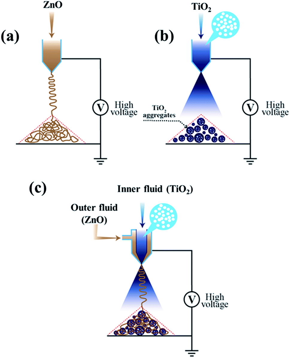 | ||
| Fig. 1 Schematic diagram of (a) e-spray process for ZnO nanofiber preparation, (b) formation of TiO2 nanobeads using e-spraying, and (c) co-axial e-spray process for the formation of hybrid films. | ||
The morphologies of all the ETMs were examined by SEM analysis. Fig. 2a exhibits the surface morphology of the ZnO NFs prepared by the electrospinning process. It shows a smooth fiber like structure constructed with tiny ZnO nanoparticles with nanoporous structures (in inset of Fig. 2a). The average diameter of the fibers is about ∼150 nm with an average length of about ∼2 μm. The cross-sectional view of these fibers is shown in Fig. 2d, demonstrating that fibers have uniform morphology from bottom to top. In Fig. 2b, we show the SEM image of hierarchically structured TiO2 NBs with an average diameter of 200 nm obtained using a binder-free e-spray technique. The individual hierarchically structured TiO2 NBs comprising several P25 primary particles were uniformly arranged on a conductive FTO substrate (as shown in the inset of Fig. 2b). The as-sprayed TiO2 NBs were packed strongly in the ETM due to the ultrafast evaporation of the solvent during the e-spray method. Moreover, the surface of the e-sprayed TiO2 NB film was smooth without any cracks, unlike the film formed via paste methods such as screen printing or doctor blading. The hierarchically structured TiO2 NBs exhibit a monodisperse and highly porous morphology which is beneficial for the better infiltration of the perovskite light absorber into the oxide ETM. Fig. 2e displays the cross-sectional SEM image of e-sprayed TiO2 NBs (∼400 nm thick) which demonstrates the uniform and tight clusters of TiO2 in the whole film. In Fig. 2c, we exhibit the surface SEM image of the hybrid ETM composed of a blend of ZnO NFs and TiO2 NBs in one set of films prepared by the co-axial e-spray method. It can be seen that TiO2 NBs are completely surrounded by the ZnO NFs which facilitate the rapid electron transport and provide a high surface area for complete pore filling of perovskite. Every single TiO2 nanobead is properly covered with ZnO NFs (in the inset of Fig. 2c). The hybrid ETM constructed with ZnO NFs + TiO2 NBs covers the whole surface of the FTO substrate as shown in the cross-sectional view of the hybrid film (Fig. 2f).
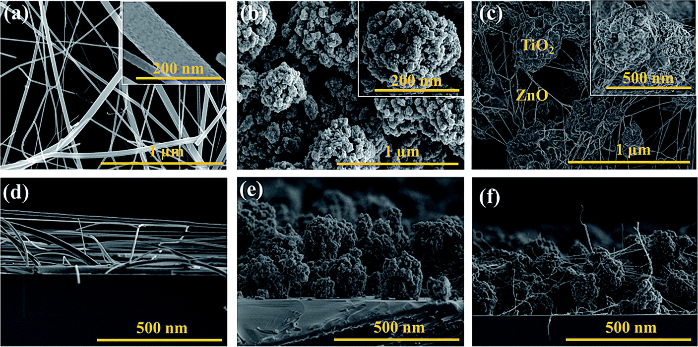 | ||
| Fig. 2 High resolution surface SEM images of (a) ZnO NFs: inset shows the magnified image of each nanofiber, (b) TiO2 NBs: inset shows the magnified view of individual nanobeads, (c) blend of ZnO NFs and TiO2 NBs; inset displays the magnified view of nanobeads surrounded by nanofibers and cross-sectional SEM images of (d) ZnO NFs, (e) TiO2 NBs, and (f) hybrid ETM of ZnO NFs and TiO2 NBs, respectively. | ||
In order to confirm the chemical compositions of ZnO fibers, an energy-dispersive X-ray analyzer (EDX) spectrum (Fig. S1 in the ESI†) was obtained of the ZnO fibers as shown in the SEM image (Fig. 2a). Apparently, the existence of Zn and O elements agree well with expectations. In Fig. S2,† the EDX spectrum of TiO2 NBs (obtained from the SEM image in Fig. 2b) is displayed, which confirms the presence of Ti and O elements in the film. The EDX spectrum (Fig. S3†) of the hybrid ETM consisting of ZnO NFs and TiO2 NBs obtained from the SEM image in Fig. 2c is shown. This spectrum confirms the co-existence of Zn, Ti and O elements in the entire film.
The photovoltaic properties of the PSCs constructed using each of the various ETMs (ZnO NFs, TiO2 NBs and hybrid ZnO NF + TiO2 NB films) are summarized in Fig. 3a and Table 1. PSCs based on hybrid ZnO NF + TiO2 NB films exhibited superior performance than PSCs from ZnO NFs and TiO2 NBs as shown in Table 1 and Fig. 3a. The PSCs formed with hybrid ZnO NF + TiO2 NB films (with an optimized film thickness of 450 nm) exhibit an average power conversion efficiency (PCEavg) of 16.42%, which is significantly higher than the PCEavg of the devices constructed with ZnO NFs (12.06%) and TiO2 NBs (14.34%). This attained result specifies that hybrid ZnO NF + TiO2 NB films are a promising ETM with multifunctional properties such as large surface area and rapid electron transport for PSC applications. We also trust that the improvement of the photovoltaic properties is closely related with efficient perovskite light-absorber infiltration into the tiny internal pores of TiO2 NBs and rapid charge transport due to ZnO NFs which are used to construct the hybrid ETM. The detailed parameters such as open-circuit voltage (VOC), short-circuit current density (JSC), fill factor (FF) and PCE of the corresponding devices are listed in Table 1. Moreover, the cross-sectional SEM image of a complete PSC fabricated with hybrid ZnO NF + TiO2 NB films, as shown in Fig. S4,† indicates that a reasonable amount of perovskite light-absorber can be filled into the internal and external pores of the hybrid ETM easily. This suggests that the hybrid ETM can offer a much larger contact area for perovskite as long as the perovskite light-absorber material is reasonably infiltrated into the TiO2 nanopores. It is also shown that thicknesses of the spiro-OMETAD layer and Au top electrode are about 260 and 60 nm, respectively. External quantum efficiency (EQE) curves of the corresponding devices are displayed in Fig. 3b. The integrated JSC values calculated from the EQE spectra agree with the JSC values measured from the current density vs. applied bias (J–V) plots. The PSCs based on the hybrid ETM clearly exhibit a high EQE value of 84% at 550 nm, compared to those based on the other two ETMs (ZnO NFs and TiO2 NBs).
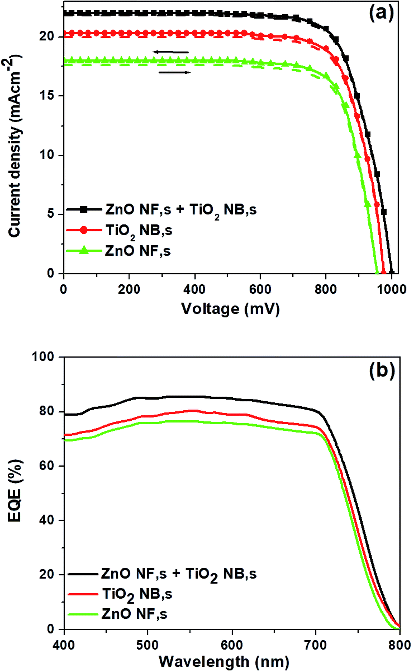 | ||
| Fig. 3 (a) J–V curves of the three different ETMs both in the forward and backward scans, and (b) EQE spectra of the corresponding ETMs, respectively. | ||
| ETM | Scan direction | J SC (mA cm−2) | V OC (mV) | FF (%) | PCEavg (%) | PCEmax (%) |
|---|---|---|---|---|---|---|
| ZnO NFs | Backward | 18.0 | 955 | 71 | 12.20 ± 0.10 | 14.62 |
| Forward | 17.6 | 955 | 71 | 11.93 ± 0.11 | 14.18 | |
| Average | 17.8 | 955 | 71 | 12.06 ± 0.10 | 14.40 | |
| TiO2 NBs | Backward | 20.3 | 975 | 73 | 14.48 ± 0.11 | 16.24 |
| Forward | 20.0 | 975 | 73 | 14.23 ± 0.10 | 16.86 | |
| Average | 20.15 | 975 | 73 | 14.34 ± 0.10 | 16.05 | |
| Hybrid ETM | Backward | 22.0 | 1000 | 75 | 16.50 ± 0.11 | 20.27 |
| Forward | 21.8 | 1000 | 75 | 16.35 ± 0.11 | 20.10 | |
| Average | 21.9 | 1000 | 75 | 16.42 ± 0.11 | 20.23 |
The effect of ETM thickness is also investigated and shown in Fig. S5.† The PSCs constructed with thicker ETMs (800 nm and 1000 nm instead of 450 nm), showed lower PCE values along with other photovoltaic parameters (Fig. S5†), showing that a lower ETM thickness is more suitable for high efficiency PSCs. The better performance of less thick ETMs is believed to be due to complete infiltration of the perovskite light-absorber into the nanopores of ETMs and to fast electron transport characteristics.
In order to reveal the effect of the hybrid ETM on the charge transfer between the perovskite and ETM layers, steady-state photoluminescence (PL) was performed by employing samples with the arrangement of glass/FTO/ZnO NFs/perovskite, glass/FTO/TiO2 NBs/perovskite, and glass/FTO/hybrid film of ZnO NFs and TiO2 NBs/perovskite, as shown in Fig. 4a. The PL peaks at 770 nm, which are associated with the intrinsic fluorescence emission of perovskite, are quenched upon contact with the hybrid film of ZnO NFs and TiO2 NBs demonstrating fast electron transfer across the interface between the perovskite films and the hybrid ETM. Moreover, compared to the other two samples, the intensity of the hybrid film of ZnO NFs and TiO2 NBs/perovskite sample is more quenched, indicating that the charge injection from the perovskite is faster for the hybrid ETM. These results clearly show that the hybrid film of ZnO NFs and TiO2 NBs is highly advantageous over the ones made of ZnO NFs and TiO2 NBs to attain effective electron injection from the perovskite absorber-layer to the ETM.
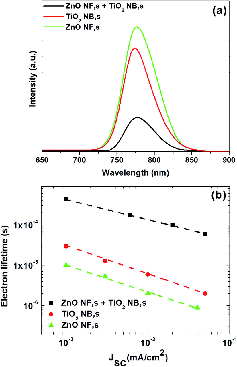 | ||
| Fig. 4 (a) Steady-state PL spectra of perovskite absorber layers formed on different ETMs, and (b) electron lifetime for the PSCs based on different ETMs, respectively. | ||
We have also measured the electron lifetime of photo-injected electrons in the ETM by pulsed light-induced transient measurement (PLITM) of the photocurrent.55,56Fig. 4b displays electron lifetime measurement as a function of JSC for the perovskite devices constructed with ETMs consisting of ZnO NFs, TiO2 NBs and the hybrid film of ZnO NFs and TiO2 NBs. It is observed that electron lifetime varies considerably depending on the type of ETMs used in the perovskite devices. In particular, the hybrid film of ZnO NFs and TiO2 NBs has the largest electron lifetime value, while ZnO NFs have the smallest numbers. The obtained result suggests that charge recombination occurs less as the ETM type changes to hybrid ETM.
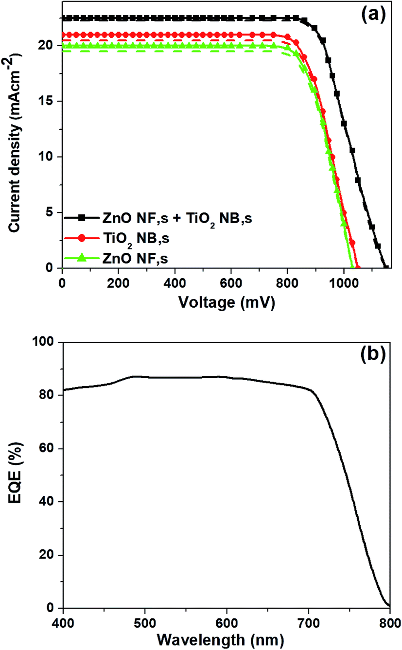
The J–V curves of the best performing perovskite devices based on three different types of ETMs such as ZnO NFs, TiO2 NBs and hybrid ZnO NF + TiO2 NB films are shown in Fig. 5a. The perovskite devices based on hybrid ZnO NF + TiO2 NB films demonstrate the highest PCE of 20.27% with a JSC of 22.91 mA cm−2, VOC of 1150 mV and FF of 77%, considered to be one of the highest values ever obtained for the typical mesoscopic PSCs based on hybrid ETMs, while the devices constructed with ZnO NFs and TiO2 NBs exhibit a maximum power conversion efficiency (PCEmax) of 14.62% and 16.24%, respectively (as shown in Fig. 5a). The EQE spectra of the best performing PSCs constructed with the hybrid ZnO NF + TiO2 NB film are shown in Fig. 5b and show the highest EQE values in the range of 350 nm to750 nm. The measured JSC of 22.9 mA cm−2 from the J–V curves (Fig. 5a) is in good agreement with the integrated JSC of 22.2 mA cm−2 as well.
 | ||
| Fig. 5 J–V curves of (a) best performing PSCs based on three different ETMs both in the forward and backward scans, and (b) EQE spectra of the champion devices based on the hybrid ETM, respectively. | ||
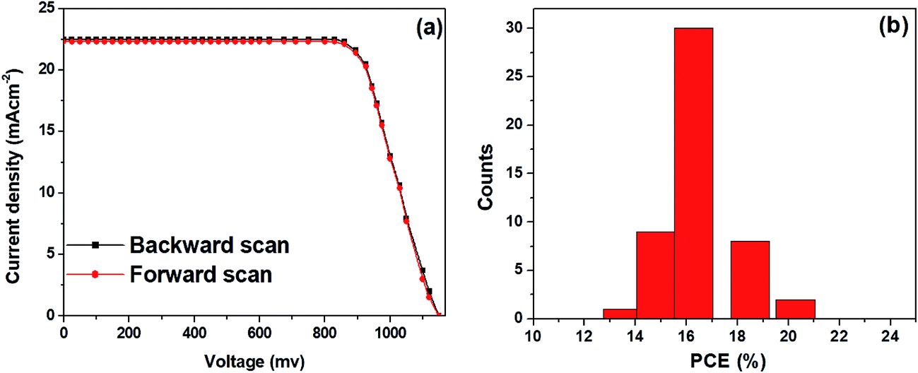
Typical J–V curves for forward and backward scans were obtained from the best performing PSCs based on the hybrid ZnO NF + TiO2 NB film are shown in Fig. 6a. A negligible hysteresis is seen in the J–V measurement. That is, the PCEs obtained by forward and backward scans were 20.1% and 20.27%, respectively. The smallest values of hysteresis rely mostly on interlayer engineering of the cells by modification of ETM types which provides the reduced surface traps inside the oxide ETM. Moreover, PSCs fabricated with the hybrid ZnO NF + TiO2 NB film show highly reproducible photovoltaic cells. As displayed in Fig. 6b, over 80% of the fabricated perovskite devices exhibit PCEs in the range of 16–20%. Conclusively, the hybrid ZnO NF + TiO2 NB film, having larger pores and enlarged surface area, is believed to be an ideal design in constructing mesoscopic PSCs with high efficiency, signifying that design of the ETM layer is also an essential topic in improving photovoltaic properties of PSCs.
 | ||
| Fig. 6 (a) J–V curves of the best performing PSCs with the hybrid ETM obtained by forward and backward scans, and (b) PCE distributions for the 50 devices of the corresponding ETM, respectively. | ||
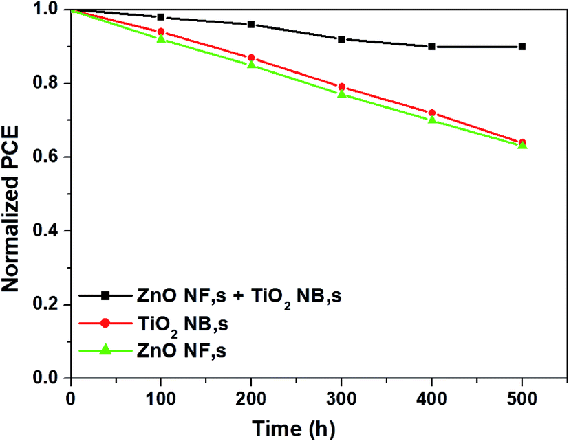
The long-term stability of the perovskite devices is also a crucial factor to be discussed from the commercialization point of view. In Fig. 7, we show the long-term stability results of perovskite devices based three different types of ETMs such as ZnO NFs, TiO2 NBs and hybrid ZnO NF + TiO2 NB films kept under ambient conditions without any encapsulation. The cells with hybrid ZnO NF + TiO2 NB films disclose superior cell stability (retains over 95% of the initial value of efficiency even after storage for 500 h) compared with other devices. The excellent cell stability is attributed to the highly porous nature of hybrid ZnO NF + TiO2 NB films which permits perfect pore filling with the perovskite light absorber inhibiting the further decomposition of perovskite.
 | ||
| Fig. 7 Long-term stability testing for three different ETMs. | ||
4. Conclusion
To summarize, a novel highly porous hybrid ETM consisting of ZnO NFs and TiO2 NBs is prepared using a viable and cost-effective coaxial electrospray method for the first time. The as-prepared films are then employed as an electron transporting layer in high efficiency, stable and hysteresis-free perovskite solar cells. The fabricated perovskite devices based on the uniquely structured hybrid ETM demonstrate a state-of-the-art PCE of 20.27% with a JSC of 22.91 mA cm−2, VOC of 1150 mV and FF of 77%, which is considerably higher than that of the perovskite devices with conventional ETMs based on nanoparticulates. The remarkable efficiency achieved is attributed to the large surface area provided by TiO2 nanobeads and fast electron transport due to ZnO nanofibers present in the hybrid ETM. PLITM measurements prove that PSCs based on the hybrid ETM exhibit considerably longer electron lifetime, which is attributed to the conquest of electron recombination initiated by the novel hybrid ETM network consisting of different oxides.Conflicts of interest
There are no conflicts to declare.Acknowledgements
The authors gratefully acknowledge the financial support from the Higher Education Commission (HEC) of Pakistan.References
- S. D. Stranks and H. J. Snaith, Nat. Nanotechnol., 2015, 10, 391–402 CrossRef CAS PubMed.
- J. H. Noh, S. H. Im, J. H. Heo, T. N. Mandal and S. I. Seok, Nano Lett., 2013, 13, 1764–1769 CrossRef CAS PubMed.
- W. S. Yang, B. W. Park, E. H. Jung, N. J. Jeon, Y. C. Kim, D. U. Lee, S. S. Shin, J. Seo, E. K. Kim, J. H. Noh and S. I. Seok, Science, 2017, 356, 1376–1379 CrossRef CAS PubMed.
- K. Mahmood, S. Sarwar and M. T. Mehran, RSC Adv., 2017, 7, 17044–17062 RSC.
- K. Mahmood and A. Khalid, Mater. Lett., 2018, 224, 78–81 CrossRef CAS.
- W. Chen, Y. Wu, J. Liu, C. Qin, X. Yang, A. Islam, Y.-B. Cheng and L. Han, Energy Environ. Sci., 2015, 8, 629–640 RSC.
- K. Mahmood, A. Khalid, F. Nawaz and M. T. Mehran, J. Colloid Interface Sci., 2018, 532, 387–394 CrossRef CAS PubMed.
- R. Zhang, D. Liu, Y. Wang, T. Zhang, X. Gu, P. Zhang, J. Wu, Z. D. Chen, Y. Zhao and S. Li, Electrochim. Acta, 2018, 265, 98–106 CrossRef CAS.
- K. Mahmood, M. T. Mehran, F. Rehman, M. S. Zafar, S. W. Ahmad and R. H. Song, ACS Omega, 2018, 3, 9648–9657 CrossRef CAS.
- K. Mahmood, A. Khalid and M. T. Mehran, Sol. Energy, 2018, 173, 496–503 CrossRef CAS.
- N. K. Noel, A. Abate, S. D. Stranks, E. S. Parrott, V. M. Burlakov, A. Goriely and H. J. Snaith, ACS Nano, 2014, 8, 9815 CrossRef CAS PubMed.
- F. Rehman, K. Mahmood, A. Khalid, M. S. Zafar and M. Hameed, J. Colloid Interface Sci., 2019, 535, 353–362 CrossRef CAS PubMed.
- X. Meng, X. Cui, M. Rager, S. Zhang, Z. Wang, J. Yu, Y. W. Harn, Z. Kang, B. K. Wanger, Y. Liu, C. Yu, J. Qiu and Z. Lin, Nano Energy, 2018, 52, 123–133 CrossRef CAS.
- M. He, B. Li, X. Cui, B. Jiang, Y. He, Y. Chen, D. O'Neil, P. Szymanski, M. A. EI-Sayed, J. Huang and Z. Lin, Nat. Commun., 2017, 8, 16045 CrossRef CAS PubMed.
- M. Ye, C. He, J. Iocozzia, X. Liu, X. Cui, X. Meng, M. Rager, X. Hong, X. Liu and Z. Lin, J. Phys. D: Appl. Phys., 2017, 50, 373002 CrossRef.
- M. He, X. Pang, X. Liu, B. Jiang, Y. He, H. Snaith and Z. Lin, Angew. Chem., Int. Ed., 2016, 55, 4280 CrossRef CAS PubMed.
- M. He, D. Zheng, M. Wang, C. Lin and Z. Lin, J. Mater. Chem. A, 2014, 2, 5994–6003 RSC.
- N. J. Jeon, J. H. Noh, W. S. Yang, Y. C. Kim, S. Ryu, J. Seo and S. I. I. Seok, Nature, 2015, 517, 476 CrossRef CAS PubMed.
- N. J. Jeon, J. H. Noh, Y. C. Kim, W. S. Yang, S. Ryu and S. I. I. Seol, Nat. Mater., 2014, 13, 897 CrossRef CAS PubMed.
- B. J. Kim, D. H. Kim, Y.-Y. Lee, H.-W. Shin, G. S. Han, J. S. Hong, K. Mahmood, T. K. Ahn, Y.-C. Joo, K. S. Hong, N.-G. Park, S. Lee and H. S. Jung, Energy Environ. Sci., 2015, 8, 916–921 RSC.
- W. Chen, Y. Wu, J. Liu, C. Qin, X. Yang, A. Islam, Y.-B. Cheng and L. Han, Energy Environ. Sci., 2015, 8, 629–640 CAS.
- K. Mahmood, B. S. Swain and A. Amassian, Adv. Mater., 2015, 27, 2859–2865 CrossRef CAS PubMed.
- J. H. Heo, D. H. Song, H. J. Han, S. Y. Kim, J. H. Kim, D. Kim, H. W. Shin, T. K. Ahn, C. Wolf, T.-W. Lee and S. H. Im, Adv. Mater., 2015, 27, 3424–3430 CAS.
- E. Edri, S. Kirmayer, A. Henning, S. Mukhopadhyay, K. Gartsman, Y. Rosenwaks, G. Hodes and D. Cahen, Nano Lett., 2014, 14, 1000–1004 CrossRef CAS PubMed.
- T. Leijtens, G. E. Eperon, S. Pathak, A. Abate, M. M. Lee and H. J. Snaith, Nat. Commun., 2013, 4, 2885 CrossRef PubMed.
- K. Wojciechowski, S. D. Stranks, A. Abate, G. Sadoughi, A. Sadhanala, N. Kopidakis, G. Rumbles, C. Z. Li, R. H. Friend, A. K. Y. Jen and H. J. Snaith, ACS Nano, 2014, 8, 12701 CrossRef CAS PubMed.
- D. Chen, F. Huang, Y.-B. Cheng and R. A. Caruso, Adv. Mater., 2009, 21, 2206–2210 CrossRef CAS.
- I. G. Yu, Y. J. Kim, H. J. Kim, C. Lee and W. I. Lee, J. Mater. Chem., 2011, 21, 532–538 RSC.
- W.-Y. Cheng, J. R. Deka, Y.-C. Chiang, A. Rogeau and S.-Y. Lu, Chem. Mater., 2012, 24, 3255–3262 CrossRef CAS.
- R. Zhou, Q. Zhang, E. Uchaker, J. Lan, M. Yin and G. Cao, J. Mater. Chem. A, 2014, 2, 2517–2525 RSC.
- T. Shu, P. Xiang, Z.-M. Zhou, H. Wang, G.-H. Liu, H.-W. Han and Y. D. Zhao, Electrochim. Acta, 2012, 68, 166–171 CrossRef CAS.
- S. D. Sung, I. Lim, P. Kang, C. Lee and W. I. Lee, Chem. Commun., 2013, 49, 6054–6056 RSC.
- H. Lee, D. Hwang, S. M. Jo, D. Kim, Y. Seo and D. Y. Kim, ACS Appl. Mater. Interfaces, 2012, 4, 3308–3315 CrossRef CAS PubMed.
- D. Hwang, H. Lee, S.-Y. Jang, S. M. Jo, D. Kim, Y. Seo and D. Y. Kim, ACS Appl. Mater. Interfaces, 2011, 3, 2719–2725 CrossRef CAS PubMed.
- F. Huang, D. Chen, X. L. Zhang, R. A. Caruso and Y.-B. Cheng, Adv. Funct. Mater., 2010, 20, 1301–1305 CrossRef CAS.
- Y. J. Kim, M. H. Lee, H. J. Kim, G. Lim, Y. S. Choi, N.-G. Park, K. Kim and W. I. Lee, Adv. Mater., 2009, 21, 3668–3673 CrossRef CAS.
- T. P. Chou, Q. Zhang, G. E. Fryxell and G. Z. Cao, Adv. Mater., 2007, 19, 2588–2592 CrossRef CAS.
- K. Mahmood, B. S. Swain and H. S. Jung, Nanoscale, 2014, 6, 9127–9138 RSC.
- A. J. Jawork, J. Mater. Sci., 2007, 42, 266–297 CrossRef.
- K. Mahmood, B. S. Swain and A. Amassian, Adv. Energy Mater., 2015, 5, 1500568 CrossRef.
- K. Mahmood, B. S. Swain, A. R. Kirmani and A. Amassian, J. Mater. Chem. A, 2015, 3, 9051–9057 RSC.
- W. Q. Wu, F. Huang, D. Chen, Y. B. Cheng and R. A. Caruso, Adv. Energy Mater., 2016, 6, 1502027 CrossRef.
- K. Mahmood, A. Khalid, M. Hameed, F. Rehman, M. T. Mehran and R. H. Song, Appl. Phys. A, 2018, 124, 824 CrossRef.
- D. Liu and T. L. Kelly, Nat. Photonics, 2014, 8, 133–138 CrossRef CAS.
- D. Li and Y. Xia, Nano Lett., 2003, 3, 555–560 CrossRef CAS.
- D. Li, J. T. McCann, Y. Xia and M. Marquezz, J. Am. Ceram. Soc., 2006, 89, 1861–1869 CrossRef CAS.
- K. Mahmood, A. Khalid, S. W. Ahmad and M. T. Mehran, Surf. Coat. Technol., 2018, 352, 231–237 CrossRef CAS.
- K. Mahmood, B. S. Swain and A. Amassian, Nanoscale, 2015, 7, 12812–12819 RSC.
- P. S. Chandrasekhar and V. K. Komarala, RSC Adv., 2017, 7, 28610–28615 RSC.
- G. S. Han, Y. H. Song, Y. U. Jin, J. W. Lee, N. G. Park, B. K. Kang, J. K. Lee, I. S. Cho, D. H. Yoon and H. S. Jung, ACS Appl. Mater. Interfaces, 2015, 7, 23521–23526 CrossRef CAS PubMed.
- J. T. W. Wang, J. M. Ball, E. M. Barea, A. Abate, J. A. AlexanderWebber, J. Huang, M. Saliba, I. Mora-Sero, J. Bisquert, H. J. Snaith and R. J. Nicholas, Nano Lett., 2014, 14, 724–730 CrossRef CAS PubMed.
- Y. Cheng, Q. D. Yang, J. Xiao, Q. Xue, H. W. Li, Z. Guan, H. L. Yip and S. W. Tsang, ACS Appl. Mater. Interfaces, 2015, 7, 19986–19993 CrossRef PubMed.
- J. Burschka, N. Pellet, S.-J. Moon, R. Humphry-Baker, P. Gao, M. K. Nazeeruddin and M. Grätzel, Nature, 2013, 499, 316–319 CrossRef CAS PubMed.
- K. Mahmood, A. Khalid, M. S. Zafar, F. Rehman, M. Hameed and M. T. Mehran, J. Colloid Interface Sci., 2019, 538, 426–432 CrossRef CAS PubMed.
- J. van de Legemaat and A. J. Frank, J. Phys. Chem. B, 2001, 105, 11194–11205 CrossRef.
- K. D. Benkstein, N. Kopidakis, J. van de Legemaat and A. J. Frank, J. Phys. Chem. B, 2003, 107, 7759–7767 CrossRef CAS.
Footnotes |
| † Electronic supplementary information (ESI) available. See DOI: 10.1039/c8na00409a |
| ‡ Both the authors contributed equally to this work. |
| This journal is © The Royal Society of Chemistry 2019 |