
 Open Access Article
 This Open Access Article is licensed under a Creative Commons Attribution-Non Commercial 3.0 Unported Licence
The dielectric constant of a bilayer graphene interface
Ron
Bessler
a,
Urs
Duerig
b and
Elad
Koren
 *a
*a
aDepartment of Materials Science and Engineering, The Russell Berrie Nanotechnology Institute, Technion – Israel Institute of Technology, 3200003 Haifa, Israel. E-mail: eladk@technion.ac.il
bSwissLitho AG, Technopark 8005, Zurich, Switzerland
First published on 7th March 2019
Abstract
The interlayer relative dielectric constant, εr, of 2-dimensional (2D) materials in general and graphitic materials in particular is one of their most important physical properties, especially for electronic applications. In this work, we study the electromechanical actuation of nano-scale graphitic contacts. We find that beside the adhesive forces there are capacitive forces that scale parabolically with the potential drop across the sheared interface. We use this phenomena to measure the intrinsic dielectric constant of the bilayer graphene interface i.e. εr = 6 ± 2, which is in perfect agreement with recent theoretical predictions for multi-layer graphene structures. Our method can be generally used to extract the dielectric properties of 2D materials systems and interfaces and our results pave the way for utilizing graphitic and other 2D materials in electromechanical based applications.
One of the essential features that characterizes the electrostatic properties of materials is the dielectric constant. Properties such as capacitance, charge screening, electron–electron interaction and energy storage are fundamentally described by the ability of a material and its surroundings to re-arrange charge. In graphene, Coulomb interactions are shown to play a significant role, in particular next to the charge neutrality point where the screening length diverges.1 Systematic studies revealed the crucial role of dielectric screening in graphene to control both Fermi velocity, Vf and electron–electron interactions.2 In addition, unique phenomena such as tunable band gap in bilayer3 and trilayer4 graphene, superconducting–insulating transition,5 Coulomb drag6 and gate controlled surface plasmons7 pointing out to a strong interplay between graphene properties and external electric fields. Consequently, the value of ε of graphene has attracted large interest.8 In fact, the large range of values for ε found for graphene by different experiments1,2,9–11i.e. 2 to 15, has become a subject of considerable debate. The ultrathin nature of graphene and the presence of substrates has definitely played a role in the experimental attempts to measure its intrinsic dielectric constant as was recently shown by angle-resolved photoemission spectroscopy (ARPES).2
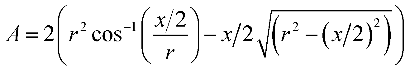
In this work, we experimentally extract the interlayer relative dielectric constant, εr, of a single bilayer graphene interface by means of electromechanical manipulation of nano-sized graphitic contacts. The graphitic structures were made of highly oriented pyrolytic graphite (HOPG) similar to our recent reports.12–15 Samples featuring cylindrical structures with a typical height of 50 nm and a diameter of 300 nm were fabricated from HOPG substrates by means of reactive ion etching, using structured Pd–Au metal layers as self-aligned shadow masks (10 and 40 nm of Pd and Au metals, respectively). We use atomic force microscopy (AFM), under ambient conditions, to shear individual nano-sized graphitic contacts and to measure the applied shear forces and current modulations during their mechanical manipulation. For electromechanical shearing, a Pt/Ir metal-coated AFM tip was cold-welded to the metal on top of the mesa by applying a force and electrical current pulse of 50 nN and 1 mA, respectively, for 1 s. Thus, we form a strong mechanical contact that allows to apply lateral shear forces of up to 200 nN and to induce a shear glide along a single basal plane in the HOPG structure (Fig. 1a). The total shear force, Ftotal, is composed of a reversible displacement force due to adhesion, Fadhesion, and to a smaller irreversible friction force, Ffriction, characterized by a force hysteresis.12 The small magnitude of Ffriction and the small force fluctuations i.e. < 10 nN, indicate that the sliding is done under superlubricity conditions12,16 (Fig. 1b). The low friction phenomenon, termed structural superlubricity,17–19 is explained by a virtually zero energy barrier due the lack of crystal symmetry in incommensurate sliding surface contacts. It can similarly be interpreted in terms of an efficient cancellation of the sliding forces experienced by different parts of the moving contact.20–23 A recent analysis of the sliding force with respect to contact area pertinent to our sliding experiments showed agreement with the observed friction forces for a rotational mismatch of about 10 degrees between the top and bottom graphene sheets.12 Along with the mechanical actuation, we apply a DC bias voltage to the AFM tip during the shearing experiment and we measure the current passing through the whole structure using a pre-amplifier that collects the current from the HOPG substrate. The current drops as the area overlap between the top and the bottom mesa structures decreases (Fig. 1b). We assign this current drop to the increase in the serial resistance of the sheared graphitic interface due to the reduced effective area overlap, in agreement with Ohm's law i.e. Rint ∝ 1/A, where Rint is the interface resistance and A is the area overlap between the top and the bottom contacts. The breaking of the mesa structure at a single glide plane was confirm by the measured lateral forces that follow the binding energy of graphite i.e. 0.223 J m−2.12 We observe an additional restoring electrostatic force, Fe that scales with the externally applied voltage, Vapplied across the sheared structure as Fe ∝ (Vapplied)n where n ≃ 2 (Fig. 2). Considering that the sheared interface comprises weakly coupled 2D graphene sheets, similar to a parallel plate capacitor, such a scaling law indicates that the measured electrostatic force has a capacitive origin. The stored electrical energy for an ideal parallel plate capacitor is  , where C = ε0εrA/d is the capacitance, V is the voltage across the plates, d is the interlayer spacing for graphite i.e. 3.4 Å, ε0 and εr are the vacuum and relative static permittivities, respectively. Thus, it can be shown that the measured electrostatic force takes the form: Fe = ε0εrr/dVint2, where r is the contact radii and Vint is the voltage drop across the sheared interface (see methods section). The quantum capacitance of multi-layer graphene contacts was recently shown to be much higher compared to the geometrical capacitance and therefore it is not considered in our model.24 We note that in cases where one of the contacts consists of less than five graphene layers, the quantum capacitance starts to play an important role and must be considered in parallel with the geometrical capacitance.25 Consequently, we can directly extract εr for the single sheared interface of the graphite contact. We extract Vint by considering the relative structural resistances, as shown by the schematic equivalent electrical circuit in the inset of Fig. 3a. The main resistive components are: 2 × RGr, Rint and Rsys, which are the graphite top and bottom mesa resistances, the sheared interface resistance and the system resistance (includes tip-sample contact resistance, AFM internal resistance, spreading resistance of the graphite pillar, cables resistance etc.), respectively. Given the ohmic responses of both RGr and Rsys, they are considered constant throughout the shearing experiment.14 Therefore, we assign the measured current modulation strictly to Rint that originates from the relative changes in the area overlap, A between the top and bottom circular contacts. We extract Rint(A), by fitting the current modulation, I(A) to the equivalent electrical circuit (Fig. 3a, inset) i.e. I(A) = Vapplied/{2 × RGr + Rsys + Rint(A)}. The lateral sliding distance, x directly relates to A according to (Fig. 2a, inset):
 | (1) |
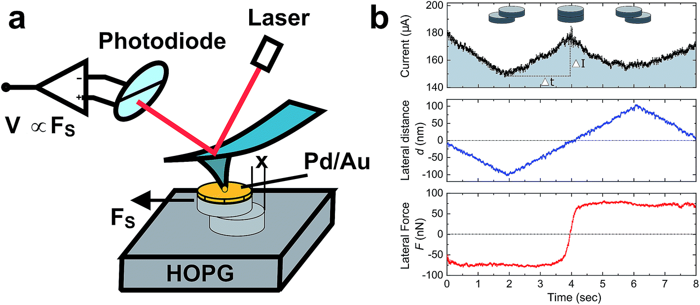 | ||
| Fig. 1 (a) Schematic illustration of the measurement setup. A conductive AFM tip is used to contact and manipulate the top part of the graphite pillar while measuring the lateral cantilever deflection and current passing through the pillar. (b) Time dependence of the measured current (top panel), lateral displacement (middle panel) and lateral force (bottom panel) during interface shearing. The circular discs in the inset of the top panel describe the relative positions of the top and bottom graphite contacts during the shearing experiment. | ||
 | ||
| Fig. 2 (a) Lateral force, Ftotal, profiles for different applied tip voltages as a function of lateral sliding distance x. Inset shows a schematic illustration of the parallel plate capacitor in which A is the effective capacitor area, x is the relative displacement from central position, d is the interlayer distance i.e. 3.4 Å and Ē is the electrostatic field. The change in the effective capacitor area during the slide creates a restoring electrostatic force Fe. (b) Absolute electrostatic force, |Fe| = |Ftotal − Fadhesion|, for different applied tip voltages as a function of lateral sliding distance (Fadhesion is the measured lateral force for zero applied voltage). | ||
 | ||
| Fig. 3 (a) Voltage drop over the sheared interface as a function of applied tip voltage. The dashed line is a linear fit showing a constant voltage ratio, Vint/Vapplied = 0.293. Vint is calculated by considering the equivalent electrical circuit shown in the inset and the current modulation throughout the sliding experiment. (b) Average measured electrostatic force for different interface potentials (symbols) and calculated profiles (solid and dashed lines) considering different interlayer dielectric constants. Best agreement is observed for εr = 6. The measured profiles in both (a) and (b) are an average of 5 different measurements and the error bars are the standard deviations. | ||
In summary, we present a new experimental method to measure the dielectric properties of a bilayer graphene interface. The approach is based on electromechanical actuation and lateral force measurement of biased graphitic mesa structures. The results are consistent with recent theoretical predictions and the method is applicable to extract the interlayer dielectric properties of 2D materials systems in general.
Methods
Lateral force constant calibration
We use the adhesion energy of graphite, σ = 0.227 [J m−2] to effectively calibrate the lateral force constant of the AFM cantilever.12 Thus, we can directly use the graphite contact radii, r to compute the measured lateral force i.e. F = 2σr.Derivation of the measured electrostatic force
The stored electrical energy for an ideal parallel plate capacitor is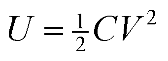 , where C = ε0εrA/d is the capacitance, V is the voltage across the plates, d is the interlayer spacing for graphite i.e. 3.4 Å, ε0 and εr are the vacuum and relative static permittivities, respectively (the vacuum permittivity ε0 = 8.85 × 10⁻¹² [F m−1]). The capacitive binding energy σe is therefore σe = U/A = ½ε0εrV2/d. The restoring electrostatic force is equal to
 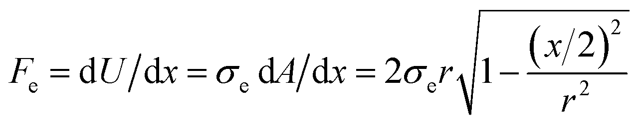 considering the derivative of eqn (1) in the main text. Thus, for short sliding distance Fe ≃ 2σer ≃ ε0εrr/dV2 and is approximately constant with respect to x. The latter expression shows that Fe scales with a power law of n = 2 with respect to the voltage-drop across the capacitor plates and is used to extract the relative dielectric constant of the sheared graphite interface εr.
Conflicts of interest
There are no conflicts to declare.Acknowledgements
We gratefully acknowledge the Israel Science Foundation (ISF) (2025261) for financial assistance and the RBNI for the nanofabrication facilities. E. K. thanks the Taub fellowship for leadership in science and technology, supported by the Taub Foundation and the Alon fellowship. We also thank Armin Knoll for stimulating discussions.References
- D. C. Elias, R. V. Gorbachev, A. S. Mayorov, S. V. Morozov, A. A. Zhukov, P. Blake, L. A. Ponomarenko, I. V. Grigorieva, K. S. Novoselov and F. Guinea, et al. Dirac Cones Reshaped by Interaction Effects in Suspended Graphene, Nat. Phys., 2011, 7, 701 Search PubMed.
- C. Hwang, D. A. Siegel, S.-K. Mo, W. Regan, A. Ismach, Y. Zhang, A. Zettl and A. Lanzara, Fermi Velocity Engineering in Graphene by Substrate Modification, Sci. Rep., 2012, 2, 590 Search PubMed.
- Y. Zhang, T.-T. Tang, C. Girit, Z. Hao, M. C. Martin, A. Zettl, M. F. Crommie, Y. R. Shen and F. Wang, Direct Observation of a Widely Tunable Bandgap in Bilayer Graphene, Nature, 2009, 459(7248), 820–823, DOI:10.1038/nature08105.
- C. H. Lui, Z. Li, K. F. Mak, E. Cappelluti and T. F. Heinz, Observation of an Electrically Tunable Band Gap in Trilayer Graphene, Nat. Phys., 2011, 7, 944 Search PubMed.
- A. Allain, Z. Han and V. Bouchiat, Electrical Control of the Superconducting-to-Insulating Transition in Graphene–metal Hybrids, Nat. Mater., 2012, 11, 590 CrossRef CAS.
- X. Liu, L. Wang, K. C. Fong, Y. Gao, P. Maher, K. Watanabe, T. Taniguchi, J. Hone, C. Dean and P. Kim, Frictional Magneto-Coulomb Drag in Graphene Double-Layer Heterostructures, Phys. Rev. Lett., 2017, 119(5), 056802, DOI:10.1103/physrevlett.119.056802.
- A. Bostwick, F. Speck, T. Seyller, K. Horn, M. Polini, R. Asgari, A. H. MacDonald and E. Rotenberg, Observation of Plasmarons in Quasi-Freestanding Doped Graphene, Science, 2010, 328(5981), 999, DOI:10.1126/science.1186489.
- E. J. G. Santos and E. Kaxiras, Electric-Field Dependence of the Effective Dielectric Constant in Graphene, Nano Lett., 2013, 13(3), 898–902, DOI:10.1021/nl303611v.
- D. A. Siegel, C.-H. Park, C. Hwang, J. Deslippe, A. V. Fedorov, S. G. Louie and A. Lanzara, Many-Body Interactions in Quasi-Freestanding Graphene, Proc. Natl. Acad. Sci., 2011, 108(28), 11365, DOI:10.1073/pnas.1100242108.
- J. D. Sanchez-Yamagishi, T. Taychatanapat, K. Watanabe, T. Taniguchi, A. Yacoby and P. Jarillo-Herrero, Quantum Hall Effect, Screening, and Layer-Polarized Insulating States in Twisted Bilayer Graphene, Phys. Rev. Lett., 2012, 108(7), 076601, DOI:10.1103/physrevlett.108.076601.
- G. E. Jellison, J. D. Hunn and H. N. Lee, Measurement of Optical Functions of Highly Oriented Pyrolytic Graphite in the Visible, Phys. Rev. B: Condens. Matter Mater. Phys., 2007, 76(8), 085125, DOI:10.1103/physrevb.76.085125.
- E. Koren, E. Lortscher, C. Rawlings, A. W. Knoll and U. Duerig, Adhesion and Friction in Mesoscopic Graphite Contacts, Science, 2015, 348(6235), 679–683, DOI:10.1126/science.aaa4157.
- E. Koren, I. Leven, E. Lörtscher, A. Knoll, O. Hod and U. Duerig, Coherent Commensurate Electronic States at the Interface between Misoriented Graphene Layers, Nat. Nanotechnol., 2016, 11(9), 752–757 CrossRef CAS PubMed.
- E. Koren, A. W. Knoll, E. Lörtscher and U. Duerig, Direct Experimental Observation of Stacking Fault Scattering in Highly Oriented Pyrolytic Graphite Meso-Structures, Nat. Commun., 2014, 5, 5837, DOI:10.1038/ncomms6837.
- E. Koren, A. W. Knoll, E. Lörtscher and U. Duerig, Meso-Scale Measurement of the Electrical Spreading Resistance in Highly Anisotropic Media, Appl. Phys. Lett., 2014, 105(12), 123112, DOI:10.1063/1.4896571.
- D. Dietzel, M. Feldmann, U. Schwarz, H. Fuchs and A. Schirmeisen, Scaling Laws of Structural Lubricity, Phys. Rev. Lett., 2013, 111(23) DOI:10.1103/physrevlett.111.235502.
- M. Hirano, K. Shinjo, R. Kaneko and Y. Murata, Anisotropy of Frictional Forces in Muscovite Mica, Phys. Rev. Lett., 1991, 67(19), 2642–2645, DOI:10.1103/physrevlett.67.2642.
- M. Hirano and K. Shinjo, Superlubricity and Frictional Anisotropy, Wear, 1993, 168(1–2), 121–125, DOI:10.1016/0043-1648(93)90207-3.
- M. Dienwiebel, G. Verhoeven, N. Pradeep, J. Frenken, J. Heimberg and H. Zandbergen, Superlubricity of Graphite, Phys. Rev. Lett., 2004, 92(12) DOI:10.1103/physrevlett.92.126101.
- M. H. Müser, L. Wenning and M. O. Robbins, Simple Microscopic Theory of Amontons's Laws for Static Friction, Phys. Rev. Lett., 2001, 86(7), 1295–1298, DOI:10.1103/physrevlett.86.1295.
- A. S. De Wijn, (In)commensurability, Scaling, and Multiplicity of Friction in Nanocrystals and Application to Gold Nanocrystals on Graphite, Phys. Rev. B: Condens. Matter Mater. Phys., 2012, 86(8) DOI:10.1103/physrevb.86.085429.
- E. Koren and U. Duerig, Moiré Scaling of the Sliding Force in Twisted Bilayer Graphene, Phys. Rev. B, 2016, 94(4) DOI:10.1103/physrevb.94.045401.
- E. Koren and U. Duerig, Superlubricity in Quasicrystalline Twisted Bilayer Graphene, Phys. Rev. B, 2016, 93(20) DOI:10.1103/physrevb.93.201404.
- C. Zhan, J. Neal, J. Wu and D. Jiang, Quantum Effects on the Capacitance of Graphene-Based Electrodes, J. Phys. Chem. C, 2015, 119(39), 22297–22303, DOI:10.1021/acs.jpcc.5b05930.
- J. Xia, F. Chen, J. Li and N. Tao, Measurement of the Quantum Capacitance of Graphene, Nat. Nanotechnol., 2009, 4, 505 CrossRef CAS PubMed.
- T. Chari, R. Ribeiro-Palau, C. R. Dean and K. Shepard, Resistivity of Rotated Graphite–Graphene Contacts, Nano Lett., 2016, 16(7), 4477–4482, DOI:10.1021/acs.nanolett.6b01657.
- A. E. Filippov, M. Dienwiebel, J. W. M. Frenken, J. Klafter and M. Urbakh, Torque and Twist against Superlubricity, Phys. Rev. Lett., 2008, 100(4), 046102, DOI:10.1103/physrevlett.100.046102.
- A. S. De Wijn, C. Fusco and A. Fasolino, Stability of Superlubric Sliding on Graphite, Phys. Rev. E: Stat., Nonlinear, Soft Matter Phys., 2010, 81(4), 046105, DOI:10.1103/physreve.81.046105.
| This journal is © The Royal Society of Chemistry 2019 |