
 Open Access Article
 This Open Access Article is licensed under a Creative Commons Attribution-Non Commercial 3.0 Unported Licence
Hybrid plasmonic Au–TiN vertically aligned nanocomposites: a nanoscale platform towards tunable optical sensing†
Xuejing
Wang
a,
Jie
Jian
a,
Susana
Diaz-Amaya
a,
Cindy E.
Kumah
c,
Ping
Lu
d,
Jijie
Huang
a,
Daw Gen
Lim
a,
Vilas G.
Pol
 b,
Jeffrey P.
Youngblood
a,
Alexandra
Boltasseva
e,
Lia A.
Stanciu
a,
Deirdre M.
O'Carroll
c,
Xinghang
Zhang
a and
Haiyan
Wang
*ae
b,
Jeffrey P.
Youngblood
a,
Alexandra
Boltasseva
e,
Lia A.
Stanciu
a,
Deirdre M.
O'Carroll
c,
Xinghang
Zhang
a and
Haiyan
Wang
*ae
aDepartment of Materials Engineering, Purdue University, West Lafayette, Indiana 47907, USA. E-mail: hwang00@purdue.edu
bDepartment of Chemical Engineering, Purdue University, West Lafayette, Indiana 47907, USA
cDepartment of Materials Science and Engineering, Rutgers University, Piscataway, New Jersey 08854, USA
dSandia National Laboratories, Albuquerque, New Mexico 87185, USA
eDepartment of Electrical Engineering, Purdue University, West Lafayette, Indiana 47907, USA
First published on 27th November 2018
Abstract
Tunable plasmonic structure at the nanometer scale presents enormous opportunities for various photonic devices. In this work, we present a hybrid plasmonic thin film platform: i.e., a vertically aligned Au nanopillar array grown inside a TiN matrix with controllable Au pillar density. Compared to single phase plasmonic materials, the presented tunable hybrid nanostructures attain optical flexibility including gradual tuning and anisotropic behavior of the complex dielectric function, resonant peak shifting and change of surface plasmon resonances (SPRs) in the UV-visible range, all confirmed by numerical simulations. The tailorable hybrid platform also demonstrates enhanced surface plasmon Raman response for Fourier-transform infrared spectroscopy (FTIR) and photoluminescence (PL) measurements, and presents great potentials as designable hybrid platforms for tunable optical-based chemical sensing applications.
Introduction
Plasmonic effects offered by metallic nanostructures in subwavelength scale enable strong light confinement or directional light routing that are unprecedented from their bulk counterparts.1 Applications using such phenomena include plasmonic waveguides,2,3 enhanced light trapping in photovoltaics,4,5 photocatalysis,6,7 bio-medical sensing,8,9 and metal-dielectrics for different metamaterial designs (e.g. hyperbolic metamaterial, negative-indexed metamaterial, etc.).10–14 Specifically, taking advantage of plasmonic metallic nanostructures, localized surface plasmon resonance (LSPR) imaging and surface enhanced Raman scattering (SERS) overcome the detection limit of conventional spectroscopies15 in biological and chemical sensing and even allow single-molecule-level detection.16–18 Reported studies include the in vivo biological embryo evolution, membrane transport detections and tumor targeting using plasmonic nanoparticles.16,18 In addition, plasmonic nanostructures coupled to dye molecules and thin-film semiconductor layers enable enhanced light capturing or light emitting efficiency, which is promising for solar energy conversion, light-emitting devices and more applicable opportunities.4,19A key aspect in the field of plasmonic nanostructures is to manipulate light–matter interactions for optical tunability. Such tunability, achieved by tailoring the dimension, geometry and concentration of the metallic nanostructures, helps to meet crucial control requirements for photonic devices, such as resonant frequency, polarization angle or propagation directions.20 For example, Lee et al. demonstrated Au and Ag nanoparticle and nanorod assemblies and tailorable plasmonic resonance frequency and bandwidth.9 Other nanostructures including nanocubes, quasi-sphere, and pyramids, have also been explored for enhanced LSPR effects at specific optical range.21 Considering the device applications using metallic plasmonic materials (e.g. Au, Ag, Al, Cu), additional key aspects to be addressed are the thermal and mechanical stabilities, materials compatibility and optical losses.10,22 To this end, new plasmonic materials such as transition metal-nitrides (i.e. TiN, TaN, et al.) have been demonstrated as low-loss plasmonic candidates with comparable optical properties to noble metals (i.e. Au and Ag), but more mechanically and thermally stable.23–27
Indeed, the current research direction is driven to metamaterial design, coupling plasmonic nanoresonators with different components, either plasmonic or dielectric.2,28,29 For example, the optical losses can be compensated by dielectric gain media for low-loss plasmonics; meanwhile, enhanced plasmonic sensitivity (Fano-resonances) was reached at a specific frequency.30 As described, hybrid plasmonic design is a straightforward approach to compensate losses from conventional noble metals. In terms of manipulating light–matter interactions, metamaterials offer novel functionalities such as hyperbolic transition,11 epsilon near zero (ENZ) and double negative properties (DNG).2,22,31–33 Currently, structures including split-ring resonators,34 double-fishnet,13 and periodic nanorod/nanowire assemblies35 down to few nanometers can be fabricated by electron beam lithography (EBL),34 focused ion beam (FIB),36 and/or with the combination of self-assembling growth methods including physical vapor deposition (PVD)29,35 and template assisted growth.21,37–39
In this work, a novel metal-nitride plasmonic material design with tailorable microstructures is presented as a tailorable hybrid material platform for tunable optical properties. The self-assembled hybrid film consists of high density, well-distributed vertically aligned Au nanopillars in the low loss titanium nitride (TiN) matrix. Both Au and TiN are plasmonic materials with plasmonic responses in neighboring wavelength regimes. Different from the previous work on Au–TaN system,26 here, we effectively controlled the Au nanopillar density, i.e. inter-spacing of the nanopillars, and thus to tune the metasurface morphology. Such tailorable hybrid thin film is expected to change the charge carrier distributions and optical properties effectively. Compared to the nanopillars (nanowires) grown by solution-based or CVD-based methods, which typically present random pillar arrangements, this self-assembled metal-nitride hybrid material platform serves as a new route in realizing hybrid plasmonic materials with well-controlled pillar morphology and density tuning. Taking advantage of such tunable Au–TiN hybrid plasmonic material, potential applications as molecule sensing based on Fourier-transform infrared spectroscopy (FTIR) measurement, enhanced Raman scattering, and enhanced photoluminescence (PL) signal have been demonstrated.
Results and discussion
To verify the overall 3D nature of the Au nanopillars in the TiN matrix, a set of transmission electron microscopy (TEM) study has been conducted on both the plan-view and cross-section TEM specimens for three different Au nanopillar densities. As shown in Fig. 1, it is clear that the Au nanopillars are growing vertically and uniformly in the TiN matrix for all cases, following the trend as marked (dashed lines) in the inset plan-vies images (a–c). The Au–TiN nanocomposite grown by the one step growth method provides the advantage of growing high crystalline nanopillar assemblies with confined diameters (average diameter of 6 nm). Selected Area Electron Diffraction (SAED) patterns are displayed as inserts in Fig. 1(d–f), from which a cube-on-cube epitaxy is confirmed for both Au and TiN phases on MgO substrates. The two phases are well separated with sharp interfaces in between. Based on the surface energy of the phases and the substrates, Au nucleates on MgO as the Volmer–Weber (VW) island and TiN nucleates as Stranski–Krastanov (2D + 3D) mode, respectively.40 Such two-phase growth has been reported previously.26,29 A schematic illustration on the vertically aligned nanocomposite (VAN) self-assembling process is described in Fig. S1.† As evidenced from the plan-view images (a–c), the nanopillar dimension and pillar spacing interplays with each other, and the overall volume fraction of the Au nanopillars maintains a gradual increase with the increase of Au density, a detailed quantification is summarized in Fig. S2 in the ESI† document. To verify phase distribution and lattice matching of the hybrid thin film, an Au–TiN sample with a lower Au density has been selected for a detailed scanning-TEM (STEM) study and the results are shown in Fig. 2. The STEM images taken under the high-angle annular dark-field (HAADF) mode from both plan-view (2a) and the cross-section (2c) reveal a very clear contrast between the Au nanopillars and the TiN matrix, where the contrast is proportional to ∼Z2, i.e., the Au nanopillars show a much brighter contrast than that of TiN because of the high Z number. In addition, the Au nanopillars grow all the way to the top film surface with very sharp interface and very straight pillar structure. The average pillar diameter for the selected sample is 3 nm. More interestingly, the distribution of the nanopillars follows a certain degree of ordering in-plane (a hexagonal-close-packed-like arrangement), with an average inter-pillar spacing of 10 nm. Such arrangement of the Au nanopillars could be preferred for well-distributed pillar spacing and density, as well as to balance the in-plane-strain between the Au and TiN phases on the underlying substrate. As evidenced from Fig. 2(d), both atomic model (inset) and the HRSTEM image show that the Au/TiN interface transitions are relatively smooth without any obvious misfit dislocations or strain contours, which demonstrates a nearly 1![[thin space (1/6-em)]](https://www.rsc.org/images/entities/char_2009.gif) :1 lattice matching between Au and TiN.
:1 lattice matching between Au and TiN.
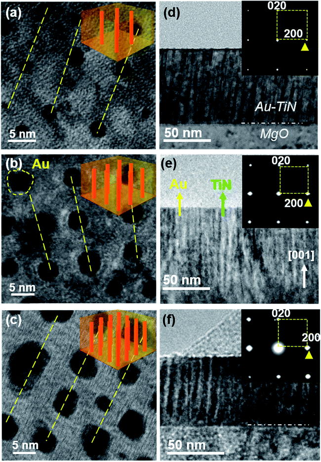 | ||
| Fig. 1 Three dimensional microstructure of Au–TiN nanocomposites grown on MgO substrates with tailored Au density. (a)–(c) Plan-view TEM images from top projections, the yellow dashed lines mark the ordering of the nanopillars. Schematic illustrations with gradual increase of Au nanopillar density are shown as insets. (d)–(f) Cross-sectional TEM images and their diffraction patterns (insets) from 〈100〉 zone axis. | ||
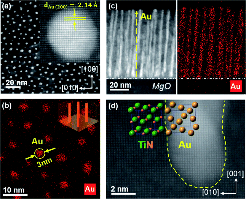 | ||
| Fig. 2 Detailed microstructure analysis of low-density Au–TiN thin film grown on MgO. (a) Plan view STEM image and high resolution of Au nanopillar top projection (inset image). (b) Plan view energy-dispersive X-ray spectroscopy (EDS) mapping of Au nanopillars, where Au is mapped as red color, inset is the illustration of low density Au–TiN hybrid platform. (c) Cross-sectional STEM and EDS mapping. (d) Cross-section HRSTEM showing the Au–TiN interface, and its atomic model. | ||
The overall growth orientation and film crystalline quality have been further explored by X-ray diffraction (XRD). Fig. S3(a)† shows the θ–2θ scans of all the films grown on (001) MgO substrates, and it is obvious that both Au and TiN phases are oriented along (00l) with a nearly perfect lattice match (<1% strain). Two phenomena are observed by comparing the Au–TiN samples with various Au compositions. First, the full-width at half maximum (FWHM) value of the TiN phase gradually increases with the increase of Au density, meanwhile (002) TiN peak is maintained close to its bulk value (2θ(002) TiN = 42.595°). On the other hand, as the Au nanopillar density increases, the (002) Au peak shifts left, approaching its bulk value of 44.363°. These observations suggest a strong vertical strain coupling between TiN and Au for the lower Au density cases. The ϕ scans (Fig. S3b†) from Au, TiN and MgO (220) planes suggest an obvious cube-on-cube relationship without any in-plane lattice rotation, which is consistent with the SAED patterns in Fig. 1. Such epitaxial nanocomposite thin film growth is also realized on c-cut sapphire substrates, as confirmed by the XRD results in Fig. S3,† with films dominated in (111) orientations.
To explore the tunable optical properties of these Au–TiN hybrid thin films with different Au nanopillar densities, normal incidence specular transmittance and reflectance spectra were collected in the wavelength range from 200 to 850 nm. An optical model was built using the COMSOL Wave Optics software package to retrieve the spectral responses and electric field maps for Au–TiN nanocomposite films with varied Au densities, and, to compare with the reference samples (pure TiN and pure Au films). Typical plasmonic resonances for pure TiN and Au are located at 375 nm and 500 nm, respectively. By adding Au nanopillars into the TiN matrix, the resonance peak of the nanocomposite exhibits a red shift gradually as the Au nanopillar density increases. From Fig. 3(a and b), the measured transmittance spectra (Fig. 3a) are generally in a good agreement with the simulated results (Fig. 3b), despite the facts that the peak separation is less obvious and the intensity drops due to defects in the Au–TiN nanocomposites. Depolarized reflectance spectra with 8° incidence are displayed in Fig. 3(c). Similarly, the resonance experiences a red shift and the reflectance spectrum experiences an intensity reduction (above a wavelength of ∼450 nm) as the Au nanopillar density increases, which suggests a stronger absorptance for Au–TiN hybrid nanostructure as compared to the pure TiN. Surface scattering spectra and back scattering images of pure TiN and Au–TiN samples are coupled in Fig. S4,† which indicate the metasurface are highly smooth, and appreciable specular reflectance in the visible to infrared regime is further proved. Based on the optical measurements, the wavelength of 440 nm is selected to map the electric field (along y direction) distributions of metasurface with three different Au pillar densities (Fig. 3d). The simulation has been performed with comparable dimensions to the real structure as seen from plan view TEM images (the upper pane). It is noted that the increase of the Au volume fraction causes enhanced near field interactions at metasurface and the Au/TiN interfaces.
 | ||
| Fig. 3 Optical spectra at UV-visible range and numerical simulations. (a) Specular transmittance of pure TiN, and three Au–TiN samples with increasing Au densities. (b) Simulated transmittance spectra with of five samples, including a pure 80 nm Au for reference. Pure TiN peak locates at 375 nm while pure Au locates at 500 nm, which explains the reason for the red shifting of the hybrid film spectra. (c) Reflectance spectra of five samples. (d) Plan view TEM images (upper pane) and simulated electric field map at 440 nm of hybrid plasmonic metasurface (lower pane) with three different Au densities, d is the diameter of Au nanopillar. Scale bar of upper pane represents 5 nm. | ||
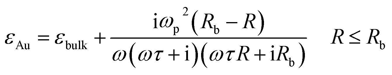
The tunable optical parameters as a function of Au nanopillar density were explored by detailed ellipsometry analysis on the films with various Au densities: 11.1 at%, 15.4 at%, 16.7 at% and 28.6 at%, which are confirmed by the EDX composition analysis (Fig. S5†), while the film thickness and nanopillar diameter (6 nm) are comparable. The psi and delta in 200 to 2500 nm range with various incident angles were collected on a 200 nm Au film, pure TiN (80 nm) and Au–TiN hybrid films (40 nm) with four different densities. A B-spline model using the commercial CompletEase software package was applied to retrieve effective parameters of each film and shows a desired match with experimental results (Fig. S6e and f†). The polarized light reflectance intensities of two Au–TiN nanocomposites with high and low Au densities are shown in Fig. S6(a–d).† The resonance of the higher density Au–TiN is broadened and red shifted due to the Au addition. Next, the optical constants were retrieved from the B-Spline model. In addition, the dielectric constant of Au nanopillars from the bulk Au (εbulk) film is calculated,41
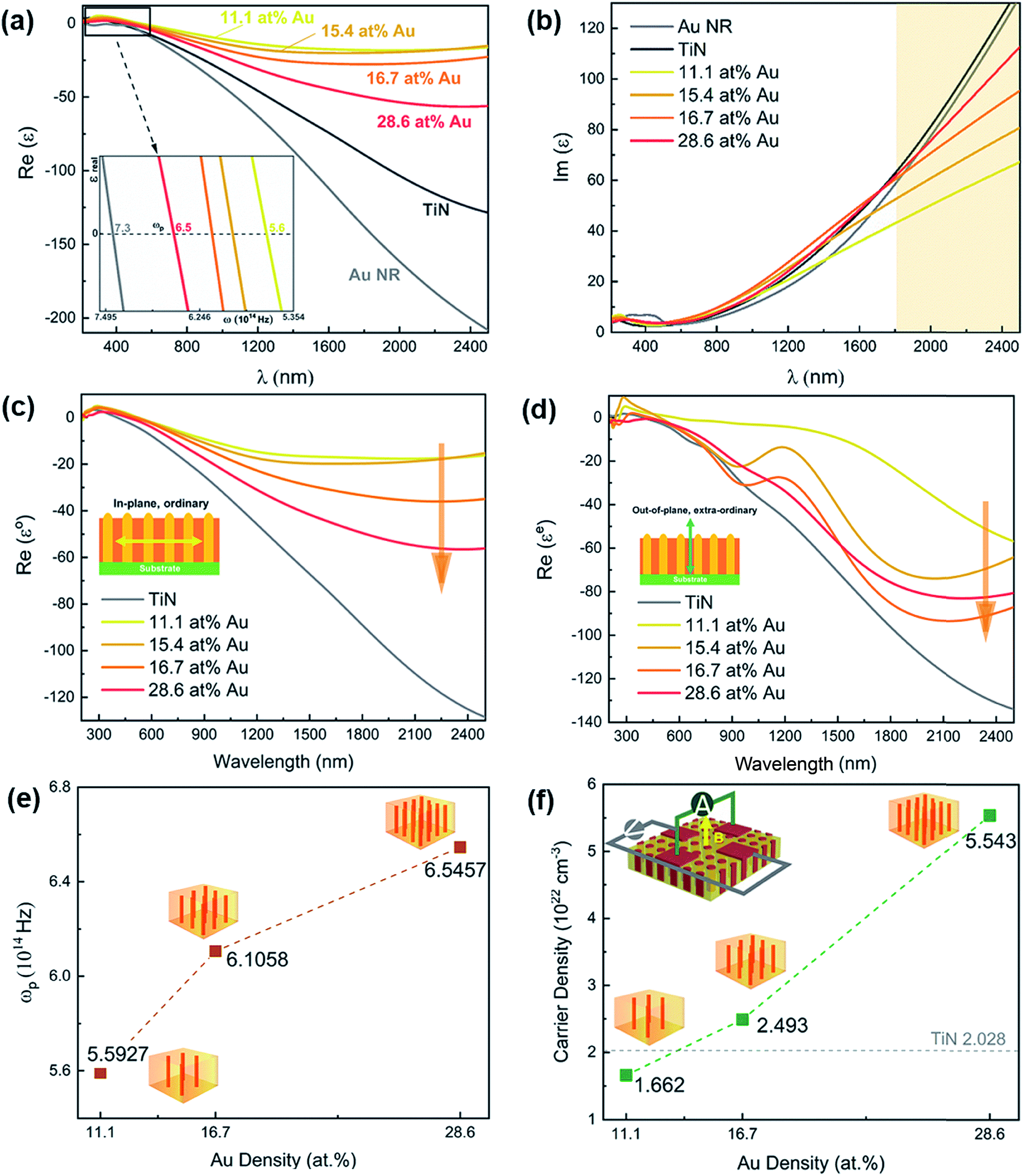 | ||
| Fig. 4 Optical constants and charge carrier density profile. (a) Real and (b) imaginary part permittivity of the listed samples: Au (r = 3 nm) nanorods (calculated), pure TiN, Au–TiN films with different Au densities (11.1 at%, 15.4 at%, 16.7 at% and 28.6 at%). (c) Ordinary (in-plane) and (d) extra-ordinary (out-of-plane) real part dielectric constants. (e) Plasma frequency as a function of three Au densities: 11.1 at%, 16.7 at% and 28.6 at% and (f) their carrier densities from Hall measurements. Pure TiN (gray dashed line) carrier density is shown as reference, and the inset is the illustration of Hall experiment setup. | ||
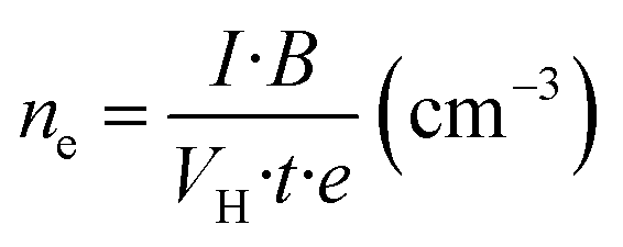
Plasma frequencies retrieved from ε1 are plotted as a function of Au density in Fig. 4(e). The shift from 5.6 ×10¹⁴ Hz (11.1 at% Au) to 7.0 × 10¹⁴ Hz (28.6 at% Au) indicates a potential increase of electron densities introduced by higher volume ratio of Au phase. Therefore, Hall measurements were performed on three Au–TiN nanocomposites with 11.1 at%, 16.7 at% and 28.6 at% Au densities, pure TiN is measured as a reference. The measurement setup with the contact geometry is shown in Fig. S8(d).† The carrier density is calculated using the equation:
Up to this point, we have demonstrated the effective dielectric tuning offered by the tailorable nanostructure. We believe that the optical tunability demonstrated in this Au–TiN hybrid system comes from multiple factors. First, the well-aligned vertical Au nanopillars in TiN matrix platform presents very anisotropic light–matter interactions in vertical and lateral directions. This highly anisotropic hybrid system behaves differently from any of the two phases alone. Second, the strong interfacial coupling between the Au nanopillars and TiN matrix results in strong vertical strain coupling, enhanced optical anisotropy, effective charge carrier injection from Au to TiN and thus demonstrate effective tuning of optical property. Specifically, as the Au nanopillar density increases, the TiN matrix is more compressive out-of-plane; charge carrier density increases effectively, and therefore the hybrid system behaves more metallic optically. Further understanding on the interfacial charge carrier transfer mechanisms by density functional theory (DFT) calculations could be valuable for exploring the interfacial coupling between the Au nanopillars and the TiN matrix.
As Au nanoparticles (NPs) have been demonstrated as durable and effective chemical sensors,44 a potential application of the hybrid Au-nitride metasurfaces is bio- and molecular-sensing. As a demonstration, we have explored the sensitivity of selective binding efficiency of the low and high density Au–TiN films with target analytes (–OH). Results are shown in Fig. 5. First, the samples were washed with methanol (CH3OH) solution before the FTIR spectra being collected, the reflection dips at near 3000 cm−1 and their fingerprints (1500–500 cm−1) are present and identified as the –OH stretch. The weak dip showing at ∼3800 cm−1 belongs to the free-standing –OH stretch. To prove the high potential of the Au nanopillars for sensing, the Au nanopillars were blocked by functionalizing the surface with thiol bonds in a 3-mercaptopropionic acid (MPA) solution for 24 hours, as the Au nanopillar surface undergoes a self-assembling reaction. Detailed processes are described in “Methods”. As expected, the –OH stretching disappeared from the FTIR spectrum, with merely background noise in the corresponding spectrum region. In the final step, the samples were treated with UV light, aiming to break the thiol bonds from the functionalized surface, and the recovery of the –OH stretching of the uncovered Au nanopillars. Within 20 min exposure, the low density Au–TiN spectrum recovers almost to its original intensity while the high density Au sample recovers to ∼50%. Therefore, the high potential for chemical sensing for the Au nanopillars at the hybrid plasmonic surface was demonstrated. In addition, the reliability and effectiveness of the Au–TiN hybrid films are confirmed by comparing with the spectra from pure TiN films (Fig. S9a†), Au colloidal nanoparticles (NPs) and nanorods (NRs) (Fig. S9b†) samples. While TiN is not contributing to functionalization, it serves as a durable matrix to “stabilize” the well-distributed Au “nanoantenna” assemblies, such that the bonding is more effective and stronger signals are detected from the surface of the hybrid films. It is believed that both the plasmonic effect between the closely spaced Au–Au nanopillars and the bonding efficiency between the molecule and the Au nanopillars play the role in enhancing the FTIR signal. As compared to solution based plasmonic nanostructures, our Au–TiN hybrid plasmonic surfaces are mechanically strong and thermally robust and can be reused multiple times.
 | ||
| Fig. 5 Chemical sensing demonstration. Total internal reflection spectra on set (a) low density Au–TiN film, set (b) high density Au–TiN film. Step 1: methanol treated spectra, signature dips located at 3000 cm−1 correspond to the –OH stretch bonded with dangling Au at metasurface; step 2: spectra taken after 24 h functionalization with MPA solution. The signature dips are disappeared due to the thiol bond reaction with –OH stretch; step 3: spectra of samples after 20 minutes UV exposure which serves to break the thiol bonds. The speed of this recovering process has a dependency on Au densities. Spectra from Au colloidal nanoparticles (NPs), nanorods (NRs) as well as the pure TiN are shown in ESI† document. | ||
To further understand the enhanced plasmonic response of the Au–TiN hybrid metasurfaces, Raman spectra (Fig. S10a†) were collected for pure TiN, low and high density Au–TiN films. Results show that the overall Raman signals are strengthened with the increased Au densities. As stated, enhanced Raman signals in the Au–TiN hybrid systems are believed to be related to the well-controlled Au inter-pillar spacing therefore stronger near field interactions. In addition, the first-order acoustic peaks (Table 1 of ESI†), namely transverse acoustic (TA), longitudinal acoustic (LA), transverse optical (TO) and the second-order acoustic (2A) modes maintain comparable with varied Au densities and match with reported values of TiN.45,46 This provides a strong evidence of stable TiN stoichiometry such that the plasmonic tuning is realized by the hybrid geometry instead of a metal–semiconductor transition of TiNx. In addition, the ability of plasmonic Au–TiN nanostructures to modify PL from molecules is important for potential fluorescence sensing implementation.47–49 To this end, a pure TiN and an Au–TiN sample were spin-coated with a fluorescent conjugated polymer thin film (∼10 nm), followed by PL imaging and spectroscopy. A fluorescent thin film on glass sample was also measured as a reference. Detailed procedures are described in the “Methods” section. The PL emission spectra of the three samples upon a 365 nm laser excitation are shown in Fig. S10(c and d).† Both plasmonic films exhibited a 10 nm blue shift as well as a sharper response (smaller FWHM) of emission peaks, as compared to glass. Meanwhile, there is an obvious fluorescence quenching attributed to LSPRs (enhanced carrier densities of the Au–TiN). This can be visualized from the PL images as shown in Fig. S10(b)† whereby the plasmonic films result in weaker fluorescence from the conjugated polymer layer. On the other hand, comparing the two plasmonic films, there is a major PL enhancement by the Au–TiN hybrid compared to the TiN film alone, suggesting a plasmon-enhanced contribution to the fluorescence due to the presence of the Au nanopillars in TiN.48 The exploration of plasmonic metasurfaces and their functionalities is a first-step demonstration, more explicit studies incorporating such metasurfaces for nanophotonic device are under investigation.
Conclusion
In this work, a two-phase Au–TiN hybrid plasmonic nanostructure with tailored Au nanopillar density and tunable optical properties has been demonstrated. Both Au and TiN phases are grown epitaxially with high crystalline quality and near perfect stoichiometry with no obvious interdiffusion in between. The addition of tailorable Au phase enables optical tunability and enhanced anisotropy, including the plasmonic red shift and systematic tuning of the complex dielectric constants (ε1 and ε2) in a broad wavelength range from 210 to 2500 nm. Also, the plasmon frequency is effectively tuned as the Au density varies, which correlates to its internal carrier density variation of the metallic nanostructures. As compared to colloidal Au NPs or NRs, our demonstration on the high chemical sensitivity and plasmon enhanced properties of the nanocomposite structures based on the FTIR, Raman and PL measurements suggest the fascinating potentials of Au–TiN hybrid thin film as robust and reusable functional SERS substrates for sensing and nanophotonic devices.Methods
Sample fabrication
Self-assembled nanocomposite Au–TiN thin films were grown on single crystalline MgO (001) and c-cut sapphire (α-Al2O3) substrates. Deposition was carried on a pulsed laser deposition (PLD) system with KrF excimer laser (Lambda Physik Compex Pro 205, λ = 248 nm, 2–5 Hz). The laser beam was focused onto the target with an incident angle of 45° and an energy density of around 3.0 J cm−2. Two-phase deposition is realized by pasting Au foil piece with a TiN target. The chamber was pumped to lower than 1.0 × 10⁻⁶ mbar to provide a desired vacuum deposition condition. Substrate temperature was maintained at 600–700 °C. Deposition rate was controlled by tuning temperature and substrate to target distance. After the deposition, the chamber was cooled to room temperature at 15 °C min−1 under vacuum. Au NPs were prepared by the citrate reduction method, using gold chloride trihydrate (HAuCl4·3H2O, ≥99.9%), and trisodium citrate dihydrate (USP testing specifications) at a molar ratio of 1:3.5; Au NRs were purchased from Nanopartz.
Microstructure characterization
The microstructures of the films were characterized by X-ray diffraction (XRD) and transmission electron microscope (TEM), and scanning transmission electron microscope (STEM). XRD θ–2θ scans were performed on a Panalytical X'Pert X-ray diffractometer with Cu Kα radiation. Bright field TEM images, selected area electron diffraction (SAED) patterns and energy-dispersive X-ray spectroscopy (EDS) chemical mapping were acquired by the FEI Talos F200X TEM. High resolution STEM was carried on a modified FEI Titan microscope with an hexapole-type illumination aberration corrector. The TEM samples were prepared using a standard cross-section sample preparation procedure, including manual grinding, polishing, dimpling and an ion milling step (PIPS 691 precision ion polishing system, 4.0 keV).Optical properties
Normal incident depolarized transmittance (T%) and reflectivity (R%) spectra were measured using an optical spectrophotometer (Lambda 950 UV/Vis Spectrophotometer) with integrated sphere detector and total absolute measurement system (TAMS). Ellipsometry experiments were carried on a RC2 spectroscopic ellipsometer (J. A. Woollam Company). Three angles 30°, 45° and 60° and a spectrum range from 210–2500 nm were covered for the measurements.FTIR measurements
The samples were submerged in 50 mM 3-mercaptopropionic acid (Sigma Aldrich) ethanoli c solution for 24 hours at room temperature; after incubation, samples were washed with ethanol and DI water to remove any unreacted MPA. The successful Au-MPA self-assembling was demonstrated by irradiating the sample at a specific wavelength of 365 nm via a UV lamp UVGL-25, in order to break specifically the Au–thiol bonds formed. The functional group present before and after self-assembly were confirmed via ATR-FTIR spectroscopy using a Spectrum 100 FTIR Spectrometer (Perkin Elmer, Waltham, MA).PL, bright- and dark-field imaging
TiN and Au–TiN samples were coated with a fluorescent thin-film before PL measurements. A fluorescent conjugated polymer poly(9,9-dioctylfluorene-alt-benzothiadiazole) (F8BT) was dissolved in chloroform to a concentration of 4.2 mg mL−1 (6.3 mg of F8BT was dissolved in 1.5 mL of chloroform). The solution was heated in a water bath at 45 °C and simultaneously stirred at 5000 rpm for 15 min and then sonicated for 15 min. Finally, 50 μL of the F8BT solution was dynamically spin coated onto the samples at a spin speed of 5000 rpm for 60 seconds. The same spin coating conditions were also used to coat a cleaned glass substrate with F8BT. Prior to spin coating, the glass substrate was cleaned in an ultrasonic bath containing detergent (0.5 wt%; Sparkleen, Fischer Scientific) for 10 min., and, subsequently, in a 50:50 solution of hydrochloric acid and ethanol for 10 min. The substrate was triple rinsed in ultrapure water (Mili-Q) after each bath cleaning step. The bright-field/dark-field imaging was performed on an inverted microscope (Axio Vert.A1, Carl Zeiss Microscopy, LLC.) coupled to an imaging spectrometer (Shamrock SR303i-A, Andor Technology Ltd.). Photoluminescence imaging and spectroscopy were carried out using an excitation source (X-Cite® 120Q, Excelitas Technologies Corp.) combined with a 365 excitation filter and a 397 nm long pass filter.
Hall measurements
The Hall resistance of as-deposited films was measured by a standard four-point probe method using electrical transport option (ETO) mode of a physical property measurement system (PPMS, Quantum Design). The gold contact for electrical measurements was deposited by pulsed laser deposition (PLD) with a Au (>99.9% purity) target at room temperature.Simulation
Normal incidence transmittance and electric field map were simulated using COMSOL Multiphysics software. Wave Optics Module with frequency domain was applied. Optical constant (n and k) for pure TiN and Au was taken from fitted ellipsometry data of an 80 nm TiN film grown on MgO substrate, and a sputtered 200 nm Au film deposited on Ti buffered glass substrate, respectively. The optical model was built with dimensions of 80 nm film thickness supported on MgO substrate, nanopillar dimension and inter-pillar distances were matched with TEM results. A normal incidence depolarized electromagnetic field was applied with two ports on top and bottom of the model. Optical parameters (i.e. real and imaginary part of permittivity) are retrieved using the CompleteEase software supported by J. A. Woollam Company, with film considered as a B-Spline layer. The averaged mean square error (MSE) of data fitting is 0.842, indicating a desired match between measurements and simulations.Author contributions
This project was conceived by H. W. and the experiments were designed by H. W. and X. W. X. W. conducted sample fabrication, XRD, TEM sample preparation and imaging, optical measurements (ellipsometry and basic UV-Vis spectra) and simulations. A. B. helped with preliminary explorations on optical (UV-Vis) measurements. J. J. contributed to Hall measurements and J. H. contributed in sample fabrication. P. L performed high resolution STEM imaging. S. A. conducted FTIR sensing experiments under the supervision of L. S. C. K. performed bright & dark field optical imaging as well as the photoluminescence experiments under the supervision of D. C. D. L. helped with Raman measurements under the supervision of V. P. and J. Y. The manuscript was drafted by X. W. and H. W., all authors contributed in editing of the manuscript.Conflicts of interest
There are no conflicts to declare.Acknowledgements
The work was partially supported by the Basil R. Turner Professorship at Purdue University. The atomic scale TEM/STEM imaging effort was funded by the U.S. National Science Foundation (DMR-1565822). Sandia National Laboratories is a multi-program laboratory managed and operated by National Technology and Engineering Solutions of Sandia, LLC., a wholly owned subsidiary of Honeywell International, Inc., for the U.S. Department of Energy's National Nuclear Security Administration under contract DE-NA0003525.References
- J. A. Schuller, E. S. Barnard, W. S. Cai, Y. C. Jun, J. S. White and M. L. Brongersma, Plasmonics for extreme light concentration and manipulation, Nat. Mater., 2010, 9(3), 193–204 CrossRef CAS PubMed.
- R. F. Oulton, V. J. Sorger, D. A. Genov, D. F. P. Pile and X. Zhang, A hybrid plasmonic waveguide for subwavelength confinement and long-range propagation, Nat. Photonics, 2008, 2(8), 496–500 CrossRef CAS.
- Y. R. Fang and M. T. Sun, Nanoplasmonic waveguides: towards applications in integrated nanophotonic circuits, Light: Sci. Appl., 2015, 4, 11 Search PubMed.
- H. A. Atwater and A. Polman, Plasmonics for improved photovoltaic devices, Nat. Mater., 2010, 9(3), 205–213 CrossRef CAS PubMed.
- V. E. Ferry, L. A. Sweatlock, D. Pacifici and H. A. Atwater, Plasmonic Nanostructure Design for Efficient Light Coupling into Solar Cells, Nano Lett., 2008, 8(12), 4391–4397 CrossRef CAS PubMed.
- S. Linic, P. Christopher and D. B. Ingram, Plasmonic-metal nanostructures for efficient conversion of solar to chemical energy, Nat. Mater., 2011, 10(12), 911–921 CrossRef CAS PubMed.
- Y. Kim, J. G. Smith and P. K. Jain, Harvesting multiple electron-hole pairs generated through plasmonic excitation of Au nanoparticles, Nat. Chem., 2018, 10(7), 763–769 CrossRef CAS PubMed.
- J. N. Anker, W. P. Hall, O. Lyandres, N. C. Shah, J. Zhao and R. P. Van Duyne, Biosensing with plasmonic nanosensors, Nat. Mater., 2008, 7(6), 442–453 CrossRef CAS PubMed.
- K. S. Lee and M. A. El-Sayed, Gold and silver nanoparticles in sensing and imaging: sensitivity of plasmon response to size, shape, and metal composition, J. Phys. Chem. B, 2006, 110(39), 19220–19225 CrossRef CAS PubMed.
- A. Boltasseva and H. A. Atwater, Low-Loss Plasmonic Metamaterials, Science, 2011, 331(6015), 290–291 CrossRef CAS PubMed.
- A. Poddubny, I. Iorsh, P. Belov and Y. Kivshar, Hyperbolic metamaterials, Nat. Photonics, 2013, 7(12), 948–957 CrossRef CAS.
- V. M. Shalaev, Optical negative-index metamaterials, Nat. Photonics, 2007, 1(1), 41–48 CrossRef CAS.
- J. Valentine, S. Zhang, T. Zentgraf, E. Ulin-Avila, D. A. Genov, G. Bartal and X. Zhang, Three-dimensional optical metamaterial with a negative refractive index, Nature, 2008, 455(7211), 376 CrossRef CAS PubMed.
- C. M. Soukoulis and M. Wegener, Past achievements and future challenges in the development of three-dimensional photonic metamaterials, Nat. Photonics, 2011, 5(9), 523–530 CrossRef CAS.
- H. Ko, S. Singamaneni and V. V. Tsukruk, Nanostructured Surfaces and Assemblies as SERS Media, Small, 2008, 4(10), 1576–1599 CrossRef CAS PubMed.
- X. H. N. Xu, W. J. Brownlow, S. V. Kyriacou, Q. Wan and J. J. Viola, Real-time probing of membrane transport in living microbial cells using single nanoparticle optics and living cell imaging, Biochemistry, 2004, 43(32), 10400–10413 CrossRef CAS PubMed.
- A. D. McFarland and R. P. Van Duyne, Single silver nanoparticles as real-time optical sensors with zeptomole sensitivity, Nano Lett., 2003, 3(8), 1057–1062 CrossRef CAS.
- K. J. Lee, P. D. Nallathamby, L. M. Browning, C. J. Osgood and X. H. N. Xu, In vivo imaging of transport and biocompatibility of single silver nanoparticles in early development of zebrafish embryos, ACS Nano, 2007, 1(2), 133–143 CrossRef CAS.
- D. J. Garfield, N. J. Borys, S. M. Hamed, N. A. Torquato, C. A. Tajon, B. Tian, B. Shevitski, E. S. Barnard, Y. D. Suh, S. Aloni, J. B. Neaton, E. M. Chan, B. E. Cohen and P. J. Schuck, Enrichment of molecular antenna triplets amplifies upconverting nanoparticle emission, Nat. Photonics, 2018, 12(7), 402 CrossRef CAS.
- Y. C. Shen, D. X. Ye, I. Celanovic, S. G. Johnson, J. D. Joannopoulos and M. Soljacic, Optical Broadband Angular Selectivity, Science, 2014, 343(6178), 1499–1501 CrossRef CAS PubMed.
- M. Rycenga, C. M. Cobley, J. Zeng, W. Y. Li, C. H. Moran, Q. Zhang, D. Qin and Y. N. Xia, Controlling the Synthesis and Assembly of Silver Nanostructures for Plasmonic Applications, Chem. Rev., 2011, 111(6), 3669–3712 CrossRef PubMed.
- J. B. Khurgin, How to deal with the loss in plasmonics and metamaterials, Nat. Nanotechnol., 2015, 10(1), 2–6 CrossRef CAS PubMed.
- G. V. Naik, V. M. Shalaev and A. Boltasseva, Alternative Plasmonic Materials: Beyond Gold and Silver, Adv. Mater., 2013, 25(24), 3264–3294 CrossRef CAS PubMed.
- L. L. Gui, S. Bagheri, N. Strohfeldt, M. Hentschel, C. M. Zgrabik, B. Metzger, H. Linnenbank, E. L. Hu and H. Giessen, Nonlinear Refractory Plasmonics with Titanium Nitride Nanoantennas, Nano Lett., 2016, 16(9), 5708–5713 CrossRef CAS PubMed.
- W. Li, U. Guler, N. Kinsey, G. V. Naik, A. Boltasseva, J. G. Guan, V. M. Shalaev and A. V. Kildishev, Refractory Plasmonics with Titanium Nitride: Broadband Metamaterial Absorber, Adv. Mater., 2014, 26(47), 7959 CrossRef CAS PubMed.
- J. J. Huang, X. J. Wang, N. L. Hogan, S. X. Wu, P. Lu, Z. Fan, Y. M. Dai, B. B. Zeng, R. Starko-Bowes, J. Jian, H. Wang, L. G. Li, R. P. Prasankumar, D. Yarotski, M. Sheldon, H. T. Chen, Z. Jacob, X. H. Zhang and H. Y. Wang, Nanoscale Artificial Plasmonic Lattice in Self-Assembled Vertically Aligned Nitride-Metal Hybrid Metamaterials, Adv. Sci., 2018, 5(7), 9 Search PubMed.
- X. Wang, J. Jian, Z. Zhou, C. Fan, Y. Dai, L. Li, J. Huang, J. Sun, A. Donohue, P. Bermel, X. Zhang, H.-T. Chen and H. Wang, Self-Assembled Ag–TiN Hybrid Plasmonic Metamaterial: Tailorable Tilted Nanopillar and Optical Properties, Adv. Opt. Mater., 2018 DOI:10.1002/adom.201801180.
- S. Jahani and Z. Jacob, All-dielectric metamaterials, Nat. Nanotechnol., 2016, 11(1), 23–36 CrossRef CAS PubMed.
- L. Li, L. Sun, J. S. Gomez-Diaz, N. L. Hogan, P. Lu, F. Khatkhatay, W. Zhang, J. Jian, J. Huang, Q. Su, M. Fan, C. Jacob, J. Li, X. Zhang, Q. Jia, M. Sheldon, A. Alu, X. Li and H. Wang, Self-Assembled Epitaxial Au-Oxide Vertically Aligned Nanocomposites for Nanoscale Metamaterials, Nano Lett., 2016, 16(6), 3936–3943 CrossRef CAS PubMed.
- Z. K. Zhou, X. N. Peng, Z. J. Yang, Z. S. Zhang, M. Li, X. R. Su, Q. Zhang, X. Y. Shan, Q. Q. Wang and Z. Y. Zhang, Tuning Gold Nanorod-Nanoparticle Hybrids into Plasmonic Fano Resonance for Dramatically Enhanced Light Emission and Transmission, Nano Lett., 2011, 11(1), 49–55 CrossRef CAS PubMed.
- Y. C. Jun, J. Reno, T. Ribaudo, E. Shaner, J. J. Greffet, S. Vassant, F. Marquier, M. Sinclair and I. Brener, Epsilon-Near-Zero Strong Coupling in Metamaterial-Semiconductor Hybrid Structures, Nano Lett., 2013, 13(11), 5391–5396 CrossRef CAS PubMed.
- X. M. Li, M. H. Bi, L. Cui, Y. Z. Zhou, X. W. Du, S. Z. Qiao and J. Yang, 3D Aluminum Hybrid Plasmonic Nanostructures with Large Areas of Dense Hot Spots and Long-Term Stability, Adv. Funct. Mater., 2017, 27(10), 9 Search PubMed.
- R. G. Freeman, M. B. Hommer, K. C. Grabar, M. A. Jackson and M. J. Natan, Ag-clad Au nanoparticles: Novel aggregation, optical, and surface-enhanced Raman scattering properties, J. Phys. Chem., 1996, 100(2), 718–724 CrossRef CAS.
- N. Liu, H. C. Guo, L. W. Fu, S. Kaiser, H. Schweizer and H. Giessen, Three-dimensional photonic metamaterials at optical frequencies, Nat. Mater., 2008, 7(1), 31–37 CrossRef CAS PubMed.
- J. H. Gao, X. Z. Wu, Q. W. Li, S. Y. Du, F. Huang, L. Y. Liang, H. L. Zhang, F. Zhuge, H. T. Cao and Y. L. Song, Template-Free Growth of Well-Ordered Silver Nano Forest/Ceramic Metamaterial Films with Tunable Optical Responses, Adv. Mater., 2017, 29(16), 8 CrossRef PubMed.
- P. Zilio, M. Malerba, A. Toma, R. P. Zaccaria, A. Jacassi and F. De Angelis, Hybridization in Three Dimensions: A Novel Route toward Plasmonic Metamolecules, Nano Lett., 2015, 15(8), 5200–5207 CrossRef CAS PubMed.
- Y. Yang, J. L. Shi, G. Kawamura and M. Nogami, Preparation of Au-Ag, Ag-Au core-shell bimetallic nanoparticles for surface-enhanced Raman scattering, Scr. Mater., 2008, 58(10), 862–865 CrossRef CAS.
- E. K. Payne, K. L. Shuford, S. Park, G. C. Schatz and C. A. Mirkin, Multipole plasmon resonances in gold nanorods, J. Phys. Chem. B, 2006, 110(5), 2150–2154 CrossRef CAS PubMed.
- X. J. Wu, J. Z. Chen, C. L. Tan, Y. H. Zhu, Y. Han and H. Zhang, Controlled growth of high-density CdS and CdSe nanorod arrays on selective facets of two-dimensional semiconductor nanoplates, Nat. Chem., 2016, 8(5), 470–475 CrossRef CAS PubMed.
- M. Ohring, Materials Science of Thin Films. 2001 Search PubMed.
- R. J. Pollard, A. Murphy, W. R. Hendren, P. R. Evans, R. Atkinson, G. A. Wurtz, A. V. Zayats and V. A. Podolskiy, Optical Nonlocalities and Additional Waves in Epsilon-Near-Zero Metamaterials, Phys. Rev. Lett., 2009, 102(12), 4 CrossRef PubMed.
- W. H. H. Sachtler, G. J. H. Dorgelo. and A. A. Holscher, The work function of gold, Surf. Sci., 1966, 5(2), 221–229 CrossRef CAS.
- S. A. Vitale, J. Kedzierski, P. Healey, P. W. Wyatt and C. L. Keast, Work-Function-Tuned TiN Metal Gate FDSOI Transistors for Subthreshold Operation, IEEE Trans. Electron Devices, 2011, 58(2), 419–426 CAS.
- K. Saha, S. S. Agasti, C. Kim, X. N. Li and V. M. Rotello, Gold Nanoparticles in Chemical and Biological Sensing, Chem. Rev., 2012, 112(5), 2739–2779 CrossRef CAS PubMed.
- M. Stoehr, C. S. Shin, I. Petrov and J. E. Greene, Raman scattering from TiNx (0.67 ≤ x ≤ 1.00) single crystals grown on MgO(001), J. Appl. Phys., 2011, 110(8), 4 CrossRef.
- Y. H. Cheng, B. K. Tay, S. P. Lau, H. Kupfer and F. Richter, Substrate bias dependence of Raman spectra for TiN films deposited by filtered cathodic vacuum arc, J. Appl. Phys., 2002, 92(4), 1845–1849 CrossRef CAS.
- D. Huang, C. P. Byers, L. Y. Wang, A. L. Hoggard, B. Hoenee, S. Dominguez-Medina, S. S. Chen, W. S. Chang, C. F. Landes and S. Link, Photoluminescence of a Plasmonic Molecule, ACS Nano, 2015, 9(7), 7072–7079 CrossRef CAS.
- T. V. Shahbazyan, Theory of Plasmon-Enhanced Metal Photoluminescence, Nano Lett., 2013, 13(1), 194–198 CrossRef CAS.
- U. S. Raikar, V. B. Tangod, B. M. Mastiholi and V. J. Fulari, Fluorescence quenching using plasmonic gold nanoparticles, Opt. Commun., 2011, 284(19), 4761–4765 CrossRef CAS.
Footnote |
| † Electronic supplementary information (ESI) available. See DOI: 10.1039/c8na00306h |
| This journal is © The Royal Society of Chemistry 2019 |