
 Open Access Article
 This Open Access Article is licensed under a Creative Commons Attribution-Non Commercial 3.0 Unported Licence
Nanoscale mechanical control of surface electrical properties of manganite films with magnetic nanoparticles†
Borislav
Vasić
 *a,
Zorica
Konstantinović
b,
Elisa
Pannunzio-Miner‡
c,
Sergio
Valencia
d,
Radu
Abrudan§
e,
Radoš
Gajić
a and
Alberto
Pomar
c
*a,
Zorica
Konstantinović
b,
Elisa
Pannunzio-Miner‡
c,
Sergio
Valencia
d,
Radu
Abrudan§
e,
Radoš
Gajić
a and
Alberto
Pomar
c
aGraphene Laboratory of Center for Solid State Physics and New Materials, Institute of Physics Belgrade, University of Belgrade, Pregrevica 118, 11080 Belgrade, Serbia. E-mail: bvasic@ipb.ac.rs
bCenter for Solid State Physics and New Materials, Institute of Physics Belgrade, University of Belgrade, Pregrevica 118, 11080 Belgrade, Serbia
cInstitut de Ciència de Materials de Barcelona, ICMAB-CSIC, Campus de la UAB, 08193 Bellaterra, Spain
dHelmholtz-Zentrum Berlin für Materialien und Energie, Albert-Einstein-Str. 15, 12489 Berlin, Germany
eInstitut für Experimentalphysik/Festkörperphysik, Ruhr-Universität Bochum, 44780 Bochum, Germany
First published on 21st February 2019
Abstract
Mechanical control of electrical properties in complex heterostructures, consisting of magnetic FeOx nanoparticles on top of manganite films, is achieved using atomic force microscope (AFM) based methods. Under applied pressure of the AFM tip, drop of the electrical conductivity is observed inducing an electrically insulating state upon a critical normal load. Current and surface potential maps suggest that the switching process is mainly governed by the flexoelectric field induced at the sample surface. The relaxation process of the electrical surface potential indicates that the diffusion of oxygen vacancies from the bulk of the manganite films towards the sample surface is the dominant relaxation mechanism. The magnetic FeOx nanoparticles, staying attached to the sample surface after the rubbing, protect the underlying manganite films and provide stability of the observed resistive switching effect. The employed mechanical control gives a new freedom in the design of resistive switching devices since it does not depend on the film thickness, and biasing is not needed.
1 Introduction
Further improvement of nanoelectronic devices such as switches and memories, requires development of novel materials as well as advanced mechanisms for the dynamic control of their electrical properties. In this context, one of the most studied mechanisms is resistive switching – an electrically induced change of the resistance of various thin metal-oxide films.1–7 This research is mainly driven by possible applications in new data storage devices such as resistive random access memories.4–7In order to fully understand complex physicochemical processes during resistive switching, investigations at the nanoscale are of particular relevance, where methods based on atomic force microscopy (AFM) are prerequisite.8–11 At the same time, AFM could provide novel methods for the manipulation of resistive switching. Namely, in addition to the electrical control, strain engineering is a simple approach to tailor the electrical properties of metal oxide films.12–17 The significant coupling between the strain and the electrical properties is based on flexoelectricity (an internal electric field resulting from a strain gradient) and the inverse Vegard effect (changes of ion concentrations due to a stress).18 The flexoelectricity is typically small. However, it has recently been shown that stress and stress gradients at the nanoscale can lead to sizable effects.19–21
A large nanoscale gradient of stress can be obtained by using the tip of an AFM which has been employed for mechanically induced resistive switching22–29 and switching of ferroelectric polarization.30–36 Since purely mechanical control is independent of film thickness and biasing is not needed, it could provide new prospects for the resistive switching. While recent studies22–29 have been focused on the mechanically induced switching of homogeneous metal-oxide films, it is interesting to investigate the phenomena in the presence of nano-objects on the film surface. In this respect, nanoparticles (NPs) constitute a model system as they not only improve mechanical properties,37 but also may provide enhanced functionalities such as novel magnetotransport phenomena38 or optoelectronic capabilities,39,40 and they could serve as novel magnetic tunnel junctions41,42 or memory devices.43
Here we investigate the local mechanical control of the surface electrical properties of a heterostructure consisting of a manganite film with magnetic FeOx NPs. The AFM tip is used to generate a local stress by rubbing the sample surface, and the resulting changes in local conductivity and electrical surface potential are subsequently measured by conductive AFM (C-AFM) and Kelvin probe force microscopy (KPFM), respectively. It is shown that for a high enough normal load, the manganite surface can be switched to an insulating state. At the same time, the sample exhibits weak room-temperature magnetism due to the presence of FeOx NPs which stay well attached to the sample surface even after the rubbing at a high normal load.
2 Experimental
2.1 Sample preparation
Samples consisting of iron oxide FeOx NPs assembled onto manganite films, were grown by radio frequency (RF) magnetron sputtering on the top of (001)-oriented SrTiO3 (STO) substrates. Two manganite families were considered with very different properties, fully spin polarized La0.67Sr0.33MnO3 (LSMO) on one side and insulating La0.5Sr0.5Fe0.5Mn0.5O3 (LSFMO) thin film on the other side. Nanostructured thin films were deposited under a pure oxygen partial pressure (0.19 mbar) at a high temperature (850–900 °C) with a wide range of nominal thickness (between 20 nm and 100 nm),44 while the detailed microstructure of LSMO films can be also found in ref. 44. Iron oxide NPs have been deposited under a pure oxygen pressure of 0.06 mbar at 700 °C.2.2 Structural and magnetic characterization
The surface morphology of nanostructured thin films was characterized by field emission scanning electron microscopy (SEM) (QUANTA FEI 200 FEG-ESEM). The crystal structure of manganite films was characterized by X-ray diffraction based reciprocal space mapping using a Bruker AXS GADDS system equipped with a 2D X-ray detector.Magnetic properties were measured with a superconducting quantum interference device magnetometer (SQUID) (Quantum Design). The structural and magnetic nature of iron oxide NPs was studied by X-ray absorption spectroscopy (XAS) and X-ray magnetic circular dichroism (XMCD). The synchrotron experiments were performed at room temperature by using the ALICE chamber45 at the PM3 beamline of the electron storage ring BESSY II of the Helmholtz-Zentrum Berlin. The radiation impinged on samples at a grazing angle of 30°. The polarization of the incoming radiation was set to circular (Pc = 0.92(3)). Data were acquired across the Fe L3,2 edges by means of total electron yield. The XMCD spectrum was obtained for a fixed helicity of the incoming polarization by reversing the magnetization direction at every data point from positive to negative by means of an external magnetic field (±0.1 T). Data were obtained in magnetic remanence. XMCD was defined as the difference in the absorption for the curves obtained after applying the external magnetic field +0.1 T (β+) and −0.1 T (β−), respectively.
2.3 AFM measurements
AFM measurements were performed using an NTEGRA Prima AFM system from NT-MDT under ambient conditions. Tapping AFM mode was used for the topographic imaging. Simultaneously, phase imaging was performed by recording the phase lag of the employed AFM cantilevers.Electrical measurements were done using C-AFM and KPFM. In C-AFM, local electrical currents were measured in contact mode, while DC voltage was applied between the sample and the AFM tip. KPFM was employed to measure the contact potential difference (CPD) between the AFM tip and the sample surface. The CPD is equal to the difference in the work functions of the tip and sample. KPFM measurements were done using a standard two-pass technique. In the first pass, sample topography was measured in tapping mode. In the second pass, the AFM cantilever was lifted by 30 nm and the sum of AC and variable DC voltage was applied between the cantilever and the sample. In the second pass, the lifted probe, only electrically excited and with a switched-off mechanical feedback loop, followed the topography measured in the first pass. Then, the CPD in every point of a two-dimensional AFM image was the value of the variable DC voltage which canceled the electrically excited oscillations of the AFM cantilever in the second pass.
The procedure for the mechanical control of the surface electrical properties was the following: first, the local electrical current or CPD was measured on an area of 2 × 2 μm2, and then we switched to contact AFM mode and only the inner and central part of 1 × 1 μm2 was rubbed at an increased normal force (in the order of 1 μN), whereas after the rubbing, we switched back to C-AFM or KPFM mode, and measured either local electrical currents or electrical surface potentials, respectively, on the initial area of 2 × 2 μm2. Hereafter, the rubbing will stand for controllable scanning at increased normal load in order to induce local changes of the electrical properties.
Both AFM imaging, rubbing and electrical measurements were done using diamond coated and nitrogen doped DCP20 probes from NT-MDT. They have triangular cantilevers with the typical force constant of 48 N m−1 and a resonant frequency of 420 kHz. Diamond coatings make these probes wear resistive, while a high doping with nitrogen provides excellent conductivity. Therefore, these robust and conductive probes are suitable for the rubbing in contact AFM mode at high normal loads (in the order of μN) and subsequent AFM imaging as well as electrical measurements many times. Since C-AFM measurements were done in contact mode as well, in order to avoid any influence of the applied normal force from the AFM tip during the C-AFM scanning, these measurements were done at low normal load from 50–100 nN.
3 Results and discussion
Manganites are an important class of metal oxides, especially in the context of resistive switching, because of both magnetoresistive46,47 and electroresistive properties.48–50 Strain engineering is an additional and simple approach to tailor their properties.25,51–54 Epitaxial manganite films are usually elastically strained due to a lattice mismatch between the films and underlying substrates (STO in the considered case). This strain facilitates growth of various self-organized morphologies such as pit arrays55–57 which can serve as templates for subsequent self-assembly of NPs.44 The strain state in our films is analyzed by the asymmetric reciprocal space mapping of the reflection (103) for the nanostructured 100 nm thick LSMO film grown on top of the STO substrate (Fig. S1(a) of the ESI†). As observed previously,55 the LSMO film seems to be fully strained with the in-plane lattice constant close to a∥,STO = 3.905 Å. On the other hand, the estimated out of-plane lattice constant a⊥,LSMO = 3.882(6) Å is slightly smaller than the corresponding bulk value of 3.889 Å, as expected due to presence of a tensile strain.44,55 Nevertheless, the higher value of the out-of-plane parameter 3.882(6) Å compared with the one of the fully strained films of 3.868 Å (ref. 58) indicates the presence of a small quantity of oxygen vacancies, as previously discussed.55The AFM topographic and the corresponding phase image of the LSMO film with FeOx NPs are given in Fig. 1(a) and (b), respectively. In the topographic image, NPs are visible as bright domains. They are better resolved in the phase image, where they are dark and with a pronounced contrast compared to the underlying LSMO film. The phase images recorded in forward and backward directions were the same, implying that the observed phase difference was due to the material contrast (not just a topographic artifact) between NPs and the LSMO substrate. As a reference, an array of three NPs is marked by dashed lines in both topographic and phase images. The SEM image of the sample is depicted in Fig. 1(c). According to the SEM images, the surface coverage of the film by NPs was around 50%, while the NP size distribution is presented in Fig. 1(d) showing that the average NP size is around 60 nm.
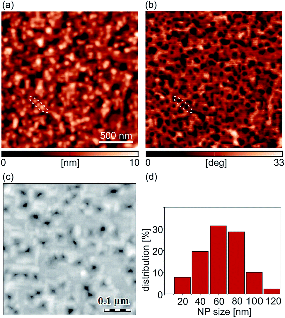 | ||
| Fig. 1 Sample morphology: (a) AFM topographic image (z-scale is 10 nm), and (b) AFM phase image acquired during the imaging in tapping mode. As an example, an array of three NPs is encircled in both the topographic and phase images. (c) SEM image and (d) the size distribution of iron-oxide NPs. | ||
The magnetic characterization reveals that iron-oxide NPs provide weak room-temperature magnetism as shown in Fig. S1(b) of the ESI.† At 300 K, the magnetization disappears in bare manganite films and remains principally only in the structures with FeOx NPs as depicted in Fig. S4 of the ESI.† According to the results of XAS and XMCD measurements, the NPs are mostly γ-Fe2O3 (the results of XAS and the fit of the XMCD curve are presented in Fig. S2 of the ESI†).
The influence of the local pressure from the AFM tip on the electrical properties of the manganite film decorated with iron-oxide NPs is presented in Fig. 2(a). The current maps were measured by C-AFM on six different 2 × 2 μm2 areas, after the rubbing of inner 1 × 1 μm2 domains with the AFM tip at increasing normal force, starting from 0.32 μN to 1.6 μN. As can be seen, after the rubbing, the electrical current of inner square domains is decreased. At a normal load of 1.6 μN, the inner square is switched to a practically insulating state (with almost zero electrical current). The histograms of the current distribution measured only on rubbed domains are given in Fig. 2(b). All current peaks are located around zero, but they become much more pronounced with increasing normal load. For the highest load, almost all points in the histogram are located around zero (just few of them with non-zero current) showing that the sample surface is really switched to an insulating state.
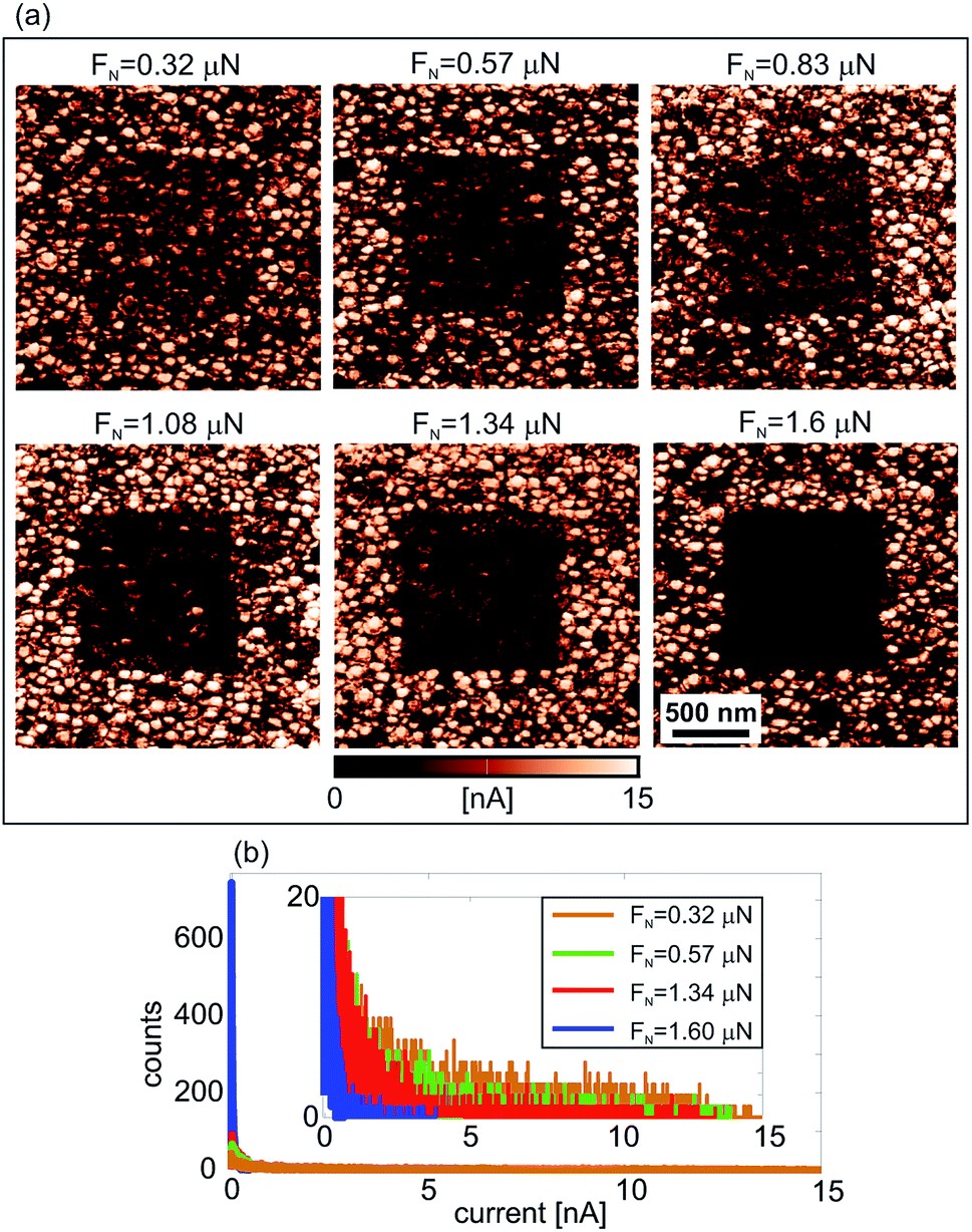 | ||
| Fig. 2 (a) 2 × 2 μm2 current maps measured by C-AFM (at the sample bias voltage Us = 2 V) after the rubbing of inner 1 × 1 μm2 domains at specified normal force (from 0.32 μN to 1.6 μN). The results were obtained on six different sample regions. The current scale is 15 nA. (b) Histograms of the current distribution on rubbed domains in (a) for the selected normal forces. In the inset, the histograms are saturated at 20 counts for a better visibility. | ||
Fig. 3(a) presents the CPD maps measured by KPFM on 2 × 2 μm2 areas after the rubbing of inner 1 × 1 μm2 regions with the AFM tip at an increasing normal force from 0.62 μN to 2.4 μN. As in the previous case, the CPD maps were measured on different sample locations. As can be seen, CPD increases on the rubbed domains. Since the CPD stands for the difference between the work functions of the AFM tip and the sample, an increase in the CPD implies a lower work function of the sample. Therefore, the KPFM results indicate the existence of an electric field originating from negative charges on the sample surface.
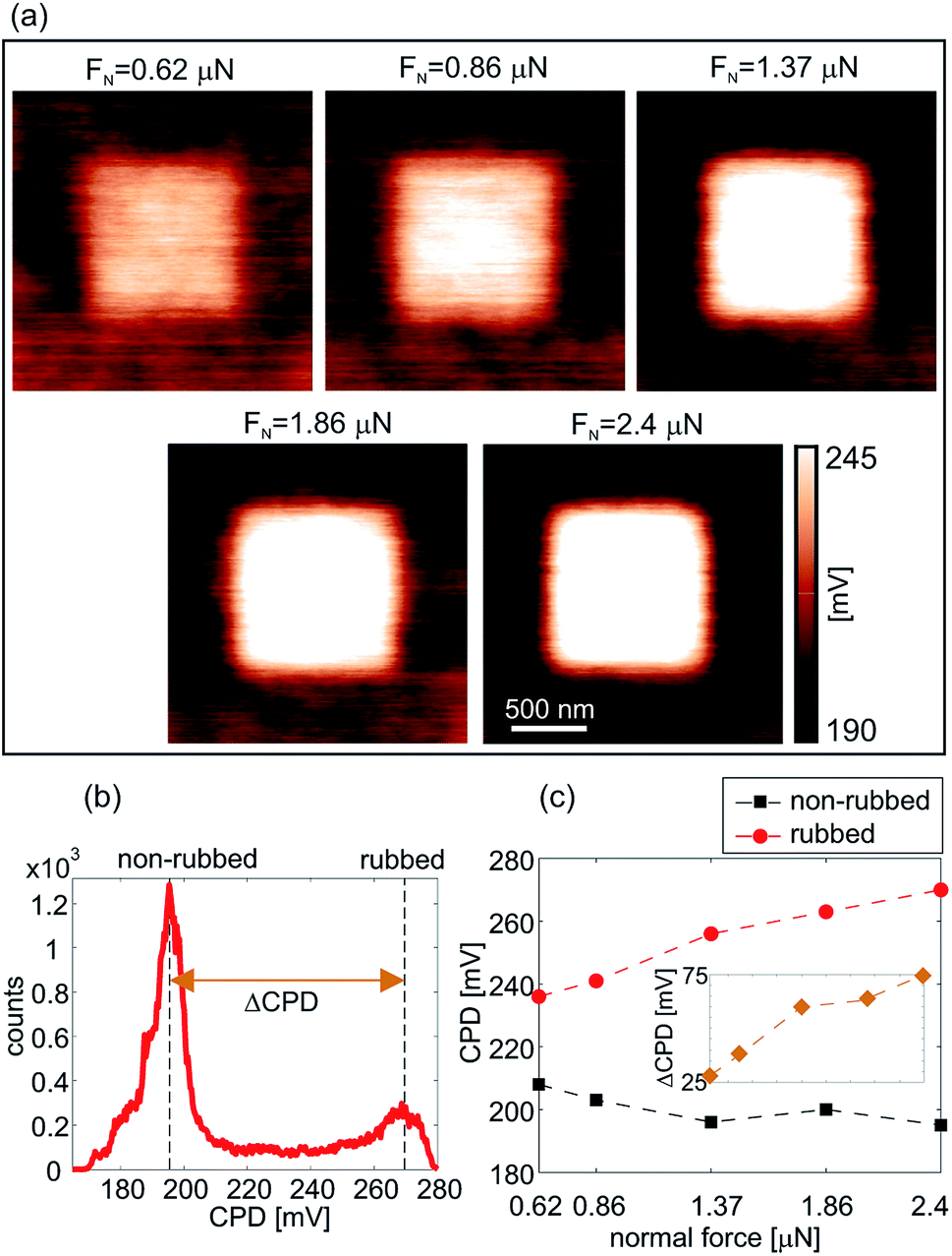 | ||
| Fig. 3 (a) 2 × 2 μm2 CPD maps measured by KPFM after the rubbing of inner 1 × 1 μm2 domain at specified normal force (from 0.62 μN to 2.4 nN). The CPD scale is 190–245 mV. (b) Histogram of the CPD distribution for a normal load of 2.4 μN. (c) Changes in the CPD and ΔCPD on rubbed and non-rubbed regions in (a) as a function of the normal force. | ||
The typical histogram of the CPD distribution is depicted in Fig. 3(b) for a normal load of 2.4 μN. There are two clearly resolved peaks corresponding to the rubbed (the peak at a higher CPD) and non-rubbed (the peak at a lower CPD) domains. Histograms were calculated for all CPD maps in this manner, whereas the histogram peaks were selected as CPD representatives as a function of a normal load. The corresponding results, together with a difference in the CPD between rubbed and non-rubbed domains (ΔCPD), are given in Fig. 3(c). As can be seen, ΔCPD continuously increases with the normal load from around 25 mV to 75 mV.
The topographic images of the sample surface before and after the rubbing (at a high normal force of 1.6 μN) are given in Fig. 4(a) and (b), respectively. The 1 × 1 μm2 rubbed domain is marked by a dashed square. The rubbed region is only slightly darker than the surrounding, non-rubbed part. The histograms and corresponding fits of the height distribution within the square domains before and after the rubbing are given in Fig. 4(c). As can be seen, the mean height is decreased by around 0.3 nm after the rubbing, meaning that the sample surface is locally compressed along the perpendicular direction. Similar results were obtained for the sample with the LSFMO film as depicted in the topographic images in Fig. S6(b) ESI,† again for the cases recorded before and after the rubbing (at a high normal force of 1.34 μN). These topographic images illustrate that NPs were not pushed away by the AFM tip during the rubbing even at very high normal loads. This was confirmed by the absence of accumulated NPs along the rims of the inner 1 × 1 μm2 rubbed domains. Still, in addition to the small local compression of the sample surface within the rubbed domains, the topographic images after the rubbing show that the height of some NPs is slightly decreased. This can be seen by lower brightness and clarity of these NPs. Therefore, NPs stay stable on the film surface and they are not removed, but some of them can be worn since their height is decreased due to local scratching. Still, the most important finding is that the NPs are tightly attached to the underlying film which stays protected.
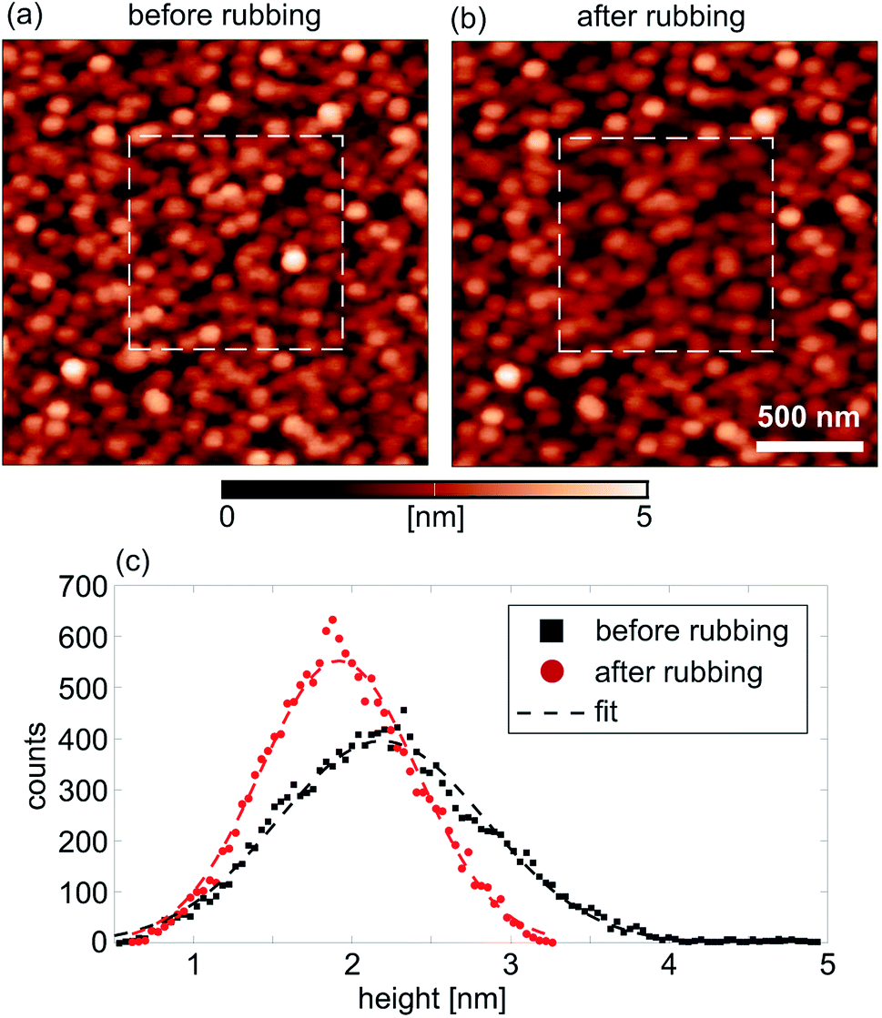 | ||
| Fig. 4 AFM topographic images of the sample surface acquired (a) before and (b) after the rubbing of the inner 1 × 1 μm2 domain (marked by dashed lines) at a normal force of 1.6 μN. z-scale is 5 nm. (c) Histogram of the height distribution within the square domains marked in parts (a) and (b). | ||
The protection by NPs is two-fold. They mechanically protect the underlying manganite film from normal load applied by the AFM probe preventing any morphological damage of the film and facilitating a stable and reliable switching process. At the same time, NPs prevent aging of manganite films due to their exposure to the environment. Namely, it is well known that environmental factors deteriorate electrical properties (conductivity for example) of thin metal-oxides, usually due to detrimental reactions with various species from the atmosphere. This is the reason why higher conductivity was usually observed on areas of the manganite film covered by NPs, as can be seen in Fig. 2(a).
In order to further explain the observed effects, the rubbing with a grounded probe at increased normal load was combined with the scanning in contact mode using a biased AFM tip, but at a low normal force. CPD maps after such manipulations are depicted in Fig. 5(a) and (b). In Fig. 5(a), the 2 × 2 μm2 square domain was firstly rubbed with the grounded tip, and then the inner 1 × 1 μm2 domain was scanned in contact mode with a bias voltage of Ut = −1 V applied to the AFM tip. In Fig. 5(b), the order was the opposite, the larger square domain was scanned in contact mode at Ut = −1 V, while the inner one was rubbed with the grounded tip. In both cases, the rubbing with the grounded tip and increased normal load leads to an increased CPD. This is exactly the opposite to the case with the applied negative voltage (in this case, the CPD was lowered). Therefore, the local pressure from the AFM probe has a similar effect as the rubbing with a positive bias voltage applied to the AFM tip.
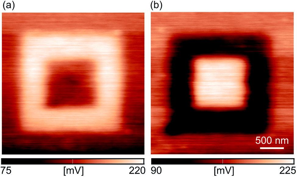 | ||
| Fig. 5 3 × 3 μm2 CPD maps of the sample rubbed with both grounded (at high normal load) and biased (low normal load and negative bias voltage) tips: (a) first, the inner 2 × 2 μm2 domain was rubbed with the grounded AFM probe and at a normal force 0.48 μN, and then, the smaller inner 1 × 1 μm2 domain was scanned in the contact mode at a low normal force 0.16 μN and with a tip bias voltage of −1 V, and (b) first, the inner 2 × 2 μm2 domain was scanned in the contact mode at a low normal force of 0.16 μN and with a tip bias voltage of −1 V, and then the smaller inner 1 × 1 μm2 domain was rubbed with the grounded AFM probe and at a normal force of 0.48 μN. The CPD scale is (a) 75–220 mV and (b) 90–225 mV. | ||
According to the type of conducting path, there are two resistive switching mechanisms: with a filamentary and an interface-type conducting path.4 The switching mechanism of LSMO films belongs to the second type and it is based on oxygen vacancy migrations.59 This mechanism is usually characterized by the formation of a Schottky barrier at the interface between a metal electrode and a semiconducting metal-oxide film.4,60 The width and height of the barrier can be tuned by applying a bias voltage which controls the oxygen vacancy concentration within the charge depletion layer at the metal–semiconductor interface.
In the considered case of mechanically induced resistive switching, instead of an externally applied bias voltage, the width and height of the Schottky barrier between the AFM tip (DCP20 probes are highly conductive, so they can be considered as metallic ones) and sample surface are controlled by the inverse Vegard effect and flexoelectric field. According to the Vegard law of a chemical expansion, the local stress and strains are proportional to the mobile ion concentration.18 Generally, the unit cell volume increases with the oxygen vacancy concentration.26 In the considered case, the sample surface rubbed with the AFM tip is locally compressed along the surface normal, so the oxygen vacancy concentration is decreased. As a result, an excess of negative charges on the sample surface appears. This is in accordance with the results of KPFM measurements, where an increased CPD was observed on rubbed parts, meaning that the Fermi level was locally raised. The electrical transport in LSMO is based on the hopping of electrons between adjacent Mn3+ and Mn4+ ions across oxygen ions.61 During the rubbing, the oxygen ion concentration beneath the tip is increased (since the oxygen vacancy concentration is decreased), so this effect does not seem to be a mechanism for the observed decrease of the electrical conductivity.
At the same time, a local and non-uniform compression of a sample surface leads to a strain gradient and a local flexoelectric field. This field is oriented from the sample surface toward the bulk.31 This pushes oxygen vacancies away from the sample surface, while attracting negative charges toward the sample surface, again in accordance with the KPFM results. Since the C-AFM maps in Fig. 2(a) were measured with a positive bias voltage applied to the sample, the induced flexoelectric field is an obstacle for the electron transport from the AFM tip to the sample. Therefore, the induced flexoelectric field makes an additional potential barrier for the electron transport resulting in lower currents as observed in the C-AFM maps.
The inverse Vegard effect and flexoelectric field can be coupled as well. The LSMO films grown on the STO substrate are under in-plane tensile strain due to a lattice mismatch as can be seen from the asymmetric reciprocal space map given in Fig. S1(a) of the ESI.† This tensile strain can induce an in-built flexoelectric field.21 The strain can be relaxed by increasing the oxygen vacancy concentration.21 However, in a sample rubbed with the AFM tip, the oxygen vacancy concentration is further decreased due to the inverse Vegard effect. The strain is then even more enhanced, potentially leading to an additional increase of the flexoelectric field. As a result, both the inverse Vegard effect and flexoelectric field could raise the potential barrier supporting the observed changes of the electrical properties.
The efficiency and robustness of the resistive switching process were tested also in the case of an insulating LSFMO thin film with FeOx NPs on top. At the same time, besides different conductivities of the underlying film (here the measured current on non-rubbed areas was up to 50 pA, that is, three order of magnitude lower than on the LSMO film with NPs), the surface coverage of the LSFMO film by NPs was increased in order to check its influence on the switching process. The asymmetric reciprocal space map and the in-plane magnetization curves for this sample are given in Figs. S3(a) and (b) of the ESI,† respectively. The morphology of the investigated sample is depicted in Fig. S5 of the ESI.† The surface coverage of the LSFMO substrate by FeOx NPs is more than 80%. As a result, the AFM tip is practically in direct contact only with the NPs (on the other hand, due to a lower surface coverage of the LSMO film, there are parts with a bare LSMO substrate which can be directly probed with the AFM tip). The influence of a local pressure on the surface electrical properties is displayed in Fig. S6 (C-AFM analysis) and S7 (KPFM analysis) of the ESI.† They illustrate that the local electrical current drops, while the local CPD grows with the normal force applied during a rubbing. The CPD maps measured after the combined rubbing with a grounded tip at an increased normal load and a negatively biased tip are given in Fig. S8 of the ESI.† The observed changes in the CPD indicate that the rubbing with the grounded tip is equivalent to the applying a positive bias voltage by the AFM tip.
According to the presented results, the electrical properties were changed in the same way for both samples despite a different surface coverage by NPs. We hence conclude that the observed changes are dominantly related to manganite films since the surface coverage by NPs does not have a significant influence. Therefore, during the rubbing with the AFM tip, the applied mechanical load is transferred across NPs to the underlying manganite films, so the AFM tip does not need to be in direct contact with the films. Since FeOx NPs are not laterally connected, electrical currents go from the AFM tip across NPs to manganite films, or directly from the tip to the films. After that, charge carriers are transported laterally through the manganite films to an external electrical contact.
The results of KPFM measurements indicate that the rubbing with a grounded AFM tip and increased normal load induce localized charges on a sample surface. In metal-oxides generally, localized charges appear due to local changes in the oxygen vacancy concentration. In order to measure the time evolution of the localized charges, the CPD was measured as a function of a time. The resulting CPD maps after the rubbing of the inner 1 × 1 μm2 square domain are given in Fig. 6(a) (immediately after the rubbing, after 2 h and after 3 h) and Fig. 6(b) (immediately after the rubbing, after 3 h and after 6 h) for LSMO and LSFMO films, respectively.
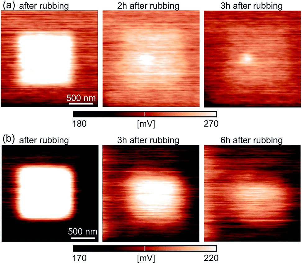 | ||
| Fig. 6 Evolution of CPD maps after the rubbing (at a normal force of 0.55 μN) of the inner 1 × 1 μm2 domain as a function of time: (a) CPD maps of the sample with a LSMO substrate measured immediately after the rubbing, after 2 h, and after 3 h, (b) CPD maps of the sample with a LSFMO substrate measured immediately after the rubbing, after 3 h, and after 6 h. The CPD scale is (a) 180–270 mV and (b) 170–220 mV. | ||
The results for the time-dependent measurements are summarized in Fig. 7(a1) and (b1) for the samples with LSMO and LSFMO films, respectively, displaying the CPD for both rubbed and non-rubbed regions. The representative values of the CPD were calculated from the corresponding histograms, as in the previous analysis. The CPD on the rubbed regions was decreasing rather slowly. After around 4 h and 6 h for the LSMO and LSFMO films, respectively, the CPD was almost equal on both rubbed and non-rubbed domains. The difference in the CPD between two domains, ΔCPD as a function of time is depicted in Fig. 7(a2) and (b2) for the LSMO and LSFMO films, respectively. The experimental results were fitted with the following curve: ΔCPD(t) = ΔCPD(0)exp(−t/τ) (given by the dashed line), where t is time in hours, while τ is the time constant of the relaxation process. For the sample with the LSMO film, τ = 1.75 h, while for that with the LSFMO film, the relaxation was much slower, with the time constant τ = 3.5 h.
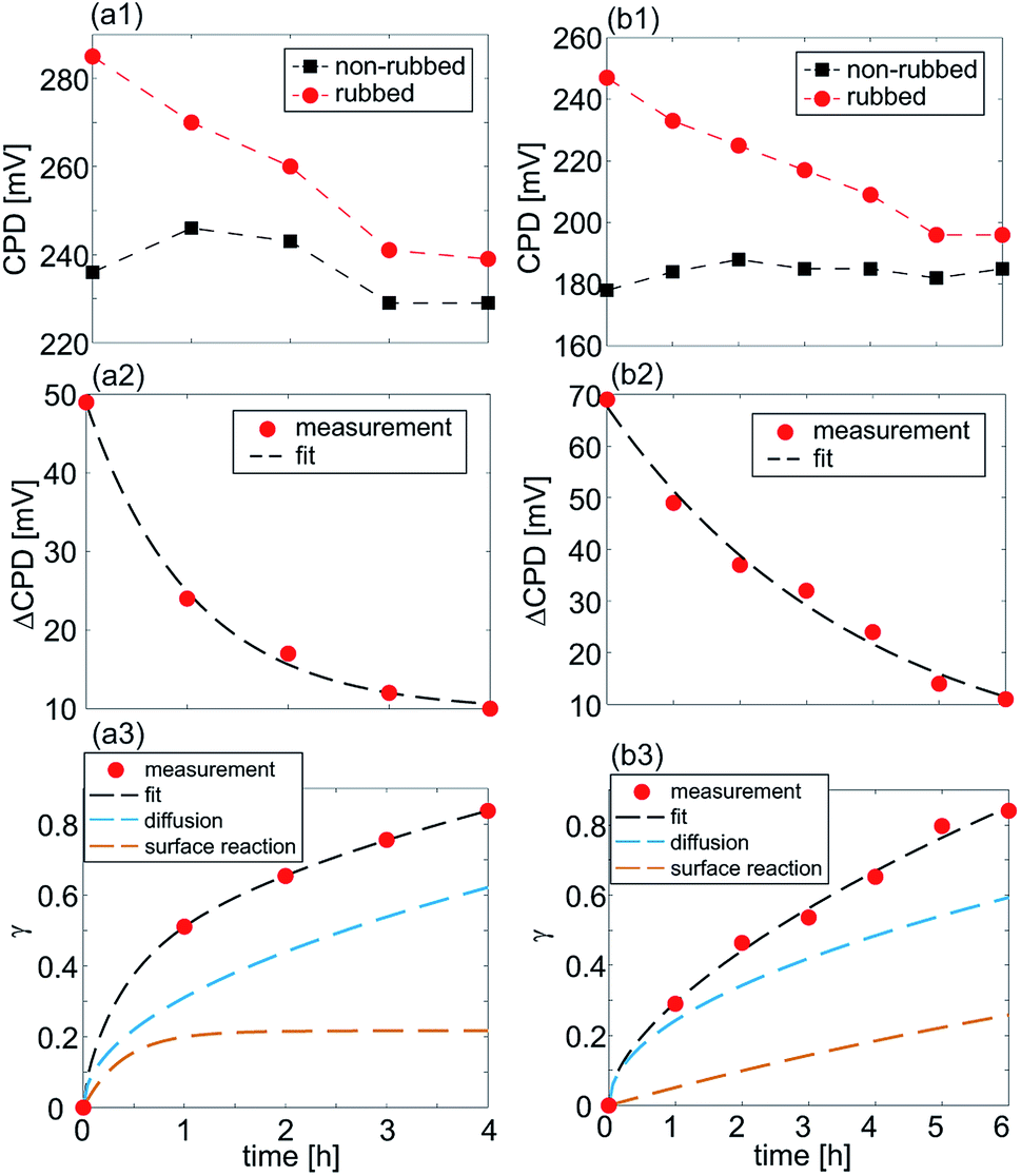 | ||
| Fig. 7 Evolution of CPD, ΔCPD, and γ as a function of time for the (a) LSMO and (b) LSFMO samples. Top row (a1) and (b1): CPD on rubbed and non-rubbed areas. Middle row (a2) and (b2): CPD difference, ΔCPD, calculated as the difference between CPDs on rubbed and non-rubbed areas. Dashed lines stand for the fit to experimentally obtained points. Bottom row (a3) and (b3): factor γ obtained from the experimental results (points) and the corresponding fit (dashed lines) with the individual contribution of γsurf(t) and γdiff(t). | ||
The rate constant of the relaxation of oxygen vacancies can be calculated according to the measured CPD in the following way:62
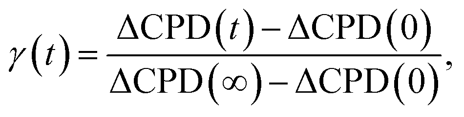 | (1) |
| γ(t) = γsurf(t) + γdiff(t), | (2) |
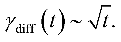 The overall rate constant γ(t) together with the contributions of γsurf(t) and γdiff(t) are given in Fig. 7(a3) and (b3) for both samples, LSMO and LSFMO films, respectively. As can be seen, the diffusion has larger contribution in the overall relaxation of oxygen vacancies. Accordingly, the relaxation process can be described in the following way. The rubbing with the AFM tip leads to a local sample compression and a decrease of the oxygen vacancy concentration at the sample surface. When the AFM tip is removed, the sample surface relaxes slowly, with a time constant in the order of hours. During that time, oxygen vacancies diffuse from the sample bulk toward the surface in order to reach the initial concentration.
KPFM maps measured after the rubbing suggest that the mechanical interaction AFM tip–sample could induce trapped charges in the sample surface due to either contact charging (local pressure in a single point) or triboelectrification (during AFM tip motion in contact with the sample). However, our measurements were done under ambient conditions at a high humidity around 50%. At such high humidity, it was not possible to observe any trapped charges induced by either contact charging or triboelectrification. Due to the conductive water layer at a sample surface, the time scale of the relaxation process of the trapped charges is very small (smaller than the time needed to switch to C-AFM (KPFM) mode and make a full scan). At the same time, the relaxation of trapped charges is generally followed by lateral charge spreading. On the other hand, in our case, we didn't observe any spreading of domains with modified surface potential as can be seen in the KPFM images in Fig. 6. In addition, tribocharges generally improve conductivity due to resulting, discharge induced currents, while we observed exactly the opposite behaviour. Therefore, decreased conductivity, the time constant of the relaxation process and clear spatial confinement of domains with the modified electrical surface potential imply that we really induced an internal flexoelectric field, while trapped charges due to triboelectrification can be excluded.
4 Conclusions
In summary, we have demonstrated mechanically induced switching of the electrical conductivity of thin manganite films covered by iron-oxide NPs. The sample surface is switched to an insulating state for a high enough local pressure applied by the AFM tip. The pressure induces the flexoelectric field while the corresponding potential barrier prevents further flow of charge carriers from the AFM tip to the sample. After removing the AFM tip, the sample surface is relaxed slowly, with the time constant in the order of hours. During this time, oxygen vacancies diffuse from the bulk of manganite films towards the surface until the equilibrium electrical surface potential is not reached. Top iron-oxide NPs provide weak room-temperature magnetism, protect the surface of manganite films from aging caused by environmental factors, and assure wear resistance and a reliable switching process of manganite films since the NPs are mechanically stable and tightly attached to the underlying manganite films even after the rubbing at high normal loads. The considered heterostructures are potential candidates for novel multifunctional devices with switchable both electric and magnetic properties. In that sense, in order to reach their full potential, the next step would be to explore the switching of their magnetic properties.Conflicts of interest
There are no conflicts to declare.Acknowledgements
B. V. and Z. K. acknowledge the support of the Serbian Ministry of Education, Science and Technological Development (Projects No. OI171005 and III45018). E. P.-M. and A. P. acknowledge financial support from the Spanish Ministry of Economy and Competitiveness through the “Severo Ochoa” Programme for Centres of Excellence in R&D (SEV-2015-0496), and project MAT2015-71664 R. This work has received funding from the European Union's Horizon 2020 research and innovation programme under the Marie Sklodowska-Curie grant agreement No. 645658 (DAFNEOX Project). B. V. thanks Dimitrije Stepanenko for fruitful discussions.References
- D. B. Strukov, G. S. Snider, D. R. Stewart and R. S. Williams, Nature, 2008, 453, 80–83 CrossRef CAS PubMed.
- J. J. Yang, M. D. Pickett, X. Li, D. A. A. Ohlberg, D. R. Stewart and R. S. Williams, Nat. Nanotechnol., 2008, 3, 429–433 CrossRef CAS PubMed.
- R. Waser and M. Aono, Nat. Mater., 2007, 6, 833–840 CrossRef CAS PubMed.
- A. Sawa, Mater. Today, 2008, 11, 28–36 CrossRef CAS.
- D. S. Jeong, R. Thomas, R. S. Katiyar, J. F. Scott, H. Kohlstedt, A. Petraru and C. S. Hwang, Rep. Prog. Phys., 2012, 75, 076502 CrossRef PubMed.
- D. B. Strukov and H. Kohlstedt, MRS Bull., 2012, 37, 108–114 CrossRef CAS.
- D. Ielmini, Semicond. Sci. Technol., 2016, 31, 063002 CrossRef.
- B. J. Choi, D. S. Jeong, S. K. Kim, C. Rohde, S. Choi, J. H. Oh, H. J. Kim, C. S. Hwang, K. Szot, R. Waser, B. Reichenberg and S. Tiedke, J. Appl. Phys., 2005, 98, 033715 CrossRef.
- K. Szot, W. Speier, G. Bihlmayer and R. Waser, Nat. Mater., 2006, 5, 312–320 CrossRef CAS PubMed.
- M. Lanza, U. Celano and F. Miao, J. Electroceram., 2017, 39, 94–108 CrossRef CAS.
- Y. Yang, X. Zhang, L. Qin, Q. Zeng, X. Qiu and R. Huang, Nat. Commun., 2017, 8, 15173 CrossRef PubMed.
- I. Bozovic, G. Logvenov, I. Belca, B. Narimbetov and I. Sveklo, Phys. Rev. Lett., 2002, 89, 107001 CrossRef CAS PubMed.
- J. H. Haeni, P. Irvin, W. Chang, R. Uecker, P. Reiche, Y. L. Li, S. Choudhury, W. Tian, M. E. Hawley, B. Craigo, A. K. Tagantsev, X. Q. Pan, S. K. Streiffer, L. Q. Chen, S. W. Kirchoefer, J. Levy and D. G. Schlom, Nature, 2004, 430, 758 CrossRef CAS PubMed.
- L. Abad, V. Laukhin, S. Valencia, A. Gaup, W. Gudat, L. Balcells and B. Martínez, Adv. Funct. Mater., 2007, 17, 3918–3925 CrossRef CAS.
- A. Tebano, C. Aruta, S. Sanna, P. G. Medaglia, G. Balestrino, A. A. Sidorenko, R. De Renzi, G. Ghiringhelli, L. Braicovich, V. Bisogni and N. B. Brookes, Phys. Rev. Lett., 2008, 100, 137401 CrossRef CAS PubMed.
- S. Lee, A. Pirogov, M. Kang, K.-H. Jang, M. Yonemura, T. Kamiyama, S.-W. Cheong, F. Gozzo, N. Shin, H. Kimura, Y. Noda and J.-G. Park, Nature, 2008, 451, 805 CrossRef CAS PubMed.
- A. Herklotz, D. Lee, E.-J. Guo, T. L. Meyer, J. R. Petrie and H. N. Lee, J. Phys.: Condens. Matter, 2017, 29, 493001 CrossRef PubMed.
- A. N. Morozovska, E. A. Eliseev, A. K. Tagantsev, S. L. Bravina, L.-Q. Chen and S. V. Kalinin, Phys. Rev. B, 2011, 83, 195313 CrossRef.
- P. Zubko, G. Catalan and A. K. Tagantsev, Annu. Rev. Mater. Res., 2013, 43, 387–421 CrossRef CAS.
- P. Zubko, G. Catalan, A. Buckley, P. R. L. Welche and J. F. Scott, Phys. Rev. Lett., 2007, 99, 167601 CrossRef CAS PubMed.
- D. Lee, A. Yoon, S. Y. Jang, J.-G. Yoon, J.-S. Chung, M. Kim, J. F. Scott and T. W. Noh, Phys. Rev. Lett., 2011, 107, 057602 CrossRef CAS PubMed.
- H. Lu, D. J. Kim, C.-W. Bark, S. Ryu, C. B. Eom, E. Y. Tsymbal and A. Gruverman, Nano Lett., 2012, 12, 6289–6292 CrossRef CAS PubMed.
- D. Lee, S. M. Yang, J.-G. Yoon and T. W. Noh, Nano Lett., 2012, 12, 6436–6440 CrossRef CAS PubMed.
- Y. Kim, S. J. Kelly, A. Morozovska, E. K. Rahani, E. Strelcov, E. Eliseev, S. Jesse, M. D. Biegalski, N. Balke, N. Benedek, D. Strukov, J. Aarts, I. Hwang, S. Oh, J. S. Choi, T. Choi, B. H. Park, V. B. Shenoy, P. Maksymovych and S. V. Kalinin, Nano Lett., 2013, 13, 4068–4074 CrossRef CAS PubMed.
- S. J. Kelly, Y. Kim, E. Eliseev, A. Morozovska, S. Jesse, M. D. Biegalski, J. F. Mitchell, H. Zheng, J. Aarts, I. Hwang, S. Oh, J. S. Choi, T. Choi, B. H. Park, S. V. Kalinin and P. Maksymovych, Nanotechnology, 2014, 25, 475302 CrossRef PubMed.
- P. Sharma, S. Ryu, J. D. Burton, T. R. Paudel, C. W. Bark, Z. Huang, Ariando, E. Y. Tsymbal, G. Catalan, C. B. Eom and A. Gruverman, Nano Lett., 2015, 15, 3547–3551 CrossRef CAS PubMed.
- Y. Wang, K. Zhao, X. Shi, G. Li, G. Xie, X. Lai, J. Ni and L. Zhang, Sci. Rep., 2015, 5, 10841 CrossRef CAS PubMed.
- S. Das, B. Wang, Y. Cao, M. Rae Cho, Y. Jae Shin, S. Mo Yang, L. Wang, M. Kim, S. V. Kalinin, L.-Q. Chen and T. W. Noh, Nat. Commun., 2017, 8, 615 CrossRef PubMed.
- A. Gómez, J. M. Vila-Fungueiriño, R. Moalla, G. Saint-Girons, J. Gázquez, M. Varela, R. Bachelet, M. Gich, F. Rivadulla and A. Carretero-Genevrier, Small, 2017, 13, 1701614 CrossRef PubMed.
- G. Catalan, A. Lubk, A. H. G. Vlooswijk, E. Snoeck, C. Magen, A. Janssens, G. Rispens, G. Rijnders, D. H. A. Blank and B. Noheda, Nat. Mater., 2011, 10, 963–967 CrossRef CAS PubMed.
- H. Lu, C.-W. Bark, D. Esque de los Ojos, J. Alcala, C. B. Eom, G. Catalan and A. Gruverman, Science, 2012, 336, 59–61 CrossRef CAS PubMed.
- Y.-J. Li, J.-J. Wang, J.-C. Ye, X.-X. Ke, G.-Y. Gou, Y. Wei, F. Xue, J. Wang, C.-S. Wang, R.-C. Peng, X.-L. Deng, Y. Yang, X.-B. Ren, L.-Q. Chen, C.-W. Nan and J.-X. Zhang, Adv. Funct. Mater., 2015, 25, 3405–3413 CrossRef CAS.
- Y. Gu, Z. Hong, J. Britson and L.-Q. Chen, Appl. Phys. Lett., 2015, 106, 022904 CrossRef.
- L. Chen, Z. Cheng, W. Xu, X. Meng, G. Yuan, J. Liu and Z. Liu, Sci. Rep., 2016, 6, 19092 CrossRef CAS PubMed.
- T. Jia, H. Kimura, Z. Cheng and H. Zhao, Sci. Rep., 2016, 6, 31867 CrossRef CAS PubMed.
- Z. Lu, Z. Fan, P. Li, H. Fan, G. Tian, X. Song, Z. Li, L. Zhao, K. Huang, F. Zhang, Z. Zhang, M. Zeng, X. Gao, J. Feng, J. Wan and J. Liu, ACS Appl. Mater. Interfaces, 2016, 8, 23963–23968 CrossRef CAS PubMed.
- D. Guo, G. Xie and J. Luo, J. Phys. D: Appl. Phys., 2014, 47, 013001 CrossRef.
- K. Yakushiji, F. Ernult, H. Imamura, K. Yamane, S. Mitani, K. Takanashi, S. Takahashi, S. Maekawa and H. Fujimori, Nat. Mater., 2005, 4, 57–61 CrossRef CAS PubMed.
- H. A. Atwater and A. Polman, Nat. Mater., 2010, 9, 205–213 CrossRef CAS PubMed.
- X. Yu, T. J. Marks and A. Facchetti, Nat. Mater., 2016, 15, 383 CrossRef CAS PubMed.
- J.-G. J. Zhu and C. Park, Mater. Today, 2006, 9, 36–45 CrossRef CAS.
- S. Yuasa, T. Nagahama, A. Fukushima, Y. Suzuki and K. Ando, Nat. Mater., 2004, 3, 868 CrossRef CAS PubMed.
- Z. Xu, M. Gao, L. Yu, L. Lu, X. Xu and Y. Jiang, ACS Appl. Mater. Interfaces, 2014, 6, 17823–17830 CrossRef CAS PubMed.
- Z. Konstantinović, F. Sandiumenge, J. Santiso, L. Balcells and B. Martínez, Nanoscale, 2013, 5, 1001–1008 RSC.
- R. Abrudan, F. Brüssing, R. Salikhov, J. Meermann, I. Radu, H. Ryll, F. Radu and H. Zabel, Rev. Sci. Instrum., 2015, 86, 063902 CrossRef CAS PubMed.
- E. Dagotto, T. Hotta and A. Moreo, Phys. Rep., 2001, 344, 1–153 CrossRef CAS.
- A.-M. Haghiri-Gosnet and J.-P. Renard, J. Phys. D: Appl. Phys., 2003, 36, R127 CrossRef CAS.
- T. Wu, S. B. Ogale, J. E. Garrison, B. Nagaraj, A. Biswas, Z. Chen, R. L. Greene, R. Ramesh, T. Venkatesan and A. J. Millis, Phys. Rev. Lett., 2001, 86, 5998–6001 CrossRef CAS PubMed.
- C. Moreno, C. Munuera, S. Valencia, F. Kronast, X. Obradors and C. Ocal, Nano Lett., 2010, 10, 3828–3835 CrossRef CAS PubMed.
- L. Balcells, L. Peña, R. Galceran, A. Pomar, B. Bozzo, Z. Konstantinović, F. Sandiumenge and B. Martínez, J. Appl. Phys., 2013, 113, 073703 CrossRef.
- A. Tebano, C. Aruta, P. G. Medaglia, F. Tozzi, G. Balestrino, A. A. Sidorenko, G. Allodi, R. De Renzi, G. Ghiringhelli, C. Dallera, L. Braicovich and N. B. Brookes, Phys. Rev. B: Condens. Matter Mater. Phys., 2006, 74, 245116 CrossRef.
- L. Marín, L. A. Rodríguez, C. Magén, E. Snoeck, R. Arras, I. Lucas, L. Morellón, P. A. Algarabel, J. M. De Teresa and M. R. Ibarra, Nano Lett., 2015, 15, 492–497 CrossRef PubMed.
- J. Ma, Y. Zhang, L. Wu, C. Song, Q. Zhang, J. Zhang, J. Ma and C.-W. Nan, MRS Commun., 2016, 6, 354–359 CrossRef CAS.
- R. U. Chandrasena, W. Yang, Q. Lei, M. U. Delgado-Jaime, K. D. Wijesekara, M. Golalikhani, B. A. Davidson, E. Arenholz, K. Kobayashi, M. Kobata, F. M. F. de Groot, U. Aschauer, N. A. Spaldin, X. Xi and A. X. Gray, Nano Lett., 2017, 17, 794–799 CrossRef CAS PubMed.
- Z. Konstantinović, J. Santiso, L. Balcells and B. Martínez, Small, 2009, 5, 265–271 CrossRef PubMed.
- Z. Konstantinović, J. Santiso, D. Colson, A. Forget, L. Balcells and B. Martínez, J. Appl. Phys., 2009, 105, 063919 CrossRef.
- Z. Konstantinović, L. Balcells and B. Martínez, J. Magn. Magn. Mater., 2010, 322, 1205–1208 CrossRef.
- A. Tebano, C. Aruta, P. G. Medaglia, F. Tozzi, G. Balestrino, A. A. Sidorenko, G. Allodi, R. De Renzi, G. Ghiringhelli, C. Dallera, L. Braicovich and N. B. Brookes, Phys. Rev. B: Condens. Matter Mater. Phys., 2006, 74, 245116 CrossRef.
- L. Yao, S. Inkinen and S. van Dijken, Nat. Commun., 2017, 8, 14544 CrossRef CAS PubMed.
- Y.-L. Chung, P. Y. Lai, Y.-C. Chen and J.-S. Chen, ACS Appl. Mater. Interfaces, 2011, 3, 1918–1924 CrossRef CAS PubMed.
- J. M. D. Coey, M. Viret and S. von Molnár, Adv. Phys., 2009, 58, 571–697 CrossRef CAS.
- M. Andra, F. Gunkel, C. Baumer, C. Xu, R. Dittmann and R. Waser, Nanoscale, 2015, 7, 14351–14357 RSC.
- T. Bieger, J. Maier and R. Waser, Sens. Actuators, B, 1992, 7, 763–768 CrossRef CAS.
- R. Merkle and J. Maier, Angew. Chem., Int. Ed., 2008, 47, 3874–3894 CrossRef CAS PubMed.
Footnotes |
| † Electronic supplementary information (ESI) available: ESI contains the reciprocal space maps of (103) reflections and in-plane magnetization curves of the LSMO film (Fig. S1), the results of XAS measurements and the resulting XMCD for the LSMO film (Fig. S2), the reciprocal space maps of (103) reflections and in-plane magnetization curves of the LSFMO film (Fig. S3), AFM images of the LSFMO film (Fig. S5), the electrical current (C-AFM images in Fig. S5) and surface potential (KPFM images in Fig. S6) distributions after the rubbing of the LSFMO film, and the maps of the electrical surface potential of the LSFMO film after combined rubbing with grounded and biased probe (KPFM images in Fig. S7). See DOI: 10.1039/c8na00301g |
| ‡ Present address: Centro de Investigaciones en Ciencias de la Tierra (CICTERRA-CONICET-UNC), Facultad de Ciencias Exactas, Físicas y Naturales, Av. Velez Sarsfield 1611, X5016GCA, Ciudad Universitaria, Cordoba, Argentina. |
| § Present address: Helmholtz-Zentrum Berlin für Materialien und Energie, Albert-Einstein-Str. 15, 12489 Berlin, Germany. |
| This journal is © The Royal Society of Chemistry 2019 |