
 Open Access Article
 This Open Access Article is licensed under a
 Creative Commons Attribution 3.0 Unported Licence
2D-MoS2 nanosheets as effective hole transport materials for colloidal PbS quantum dot solar cells†
Srikanth Reddy
Tulsani
 ab,
Arup K.
Rath
ab and
Dattatray J.
Late
*ab
ab,
Arup K.
Rath
ab and
Dattatray J.
Late
*ab
aPhysical and Materials Chemistry Division, CSIR-National Chemical Laboratory, Dr Homi Bhabha Road, Pune, 411008, India. E-mail: dj.late@ncl.res.in; datta099@gmail.com
bAcademy of Scientific and Innovative Research (AcSIR), Ghaziabad-201002, India
First published on 7th January 2019
Abstract
Herein, we demonstrate for the first time matrix-free deposition of two dimensional (2D) MoS2 nanosheets as an efficient hole transport layer (HTL) for colloidal lead sulfide (PbS) quantum dot (QD) solar cells. We have developed all-solution-processed n–p–p+ architecture solar cells where ZnO nanoparticles were used as an n-type window layer, a PbS QD layer acted as a light absorbing p-type layer and 2D-MoS2 nanosheets acted as a p+-type hole transport layer. The MoS2 nanosheets allow better interface with the PbS QD layers. The incorporation of the MoS2 hole transport layer leads to superior fill factor, higher open circuit voltage and better performance in colloidal PbS QD solar cells. These results show that one layer of MoS2 nanosheets improves the power conversion efficiency of the device from 0.92% for a hole transport material free device to 2.48%. The present work reveals the development of 2D-MoS2 nanosheets as a new hole transport layer for the fabrication of cost-effective, durable and efficient colloidal PbS quantum dot solar cells.
1 Introduction
In recent years two-dimensional (2D) transition metal dichalcogenides (TMDs) have attracted widespread attention because of their potential application in optoelectronic devices,1 catalysis,2 transistors,3–5 photonics,6–9 photodetectors,10 electronics,11 sensors,12,13 memories,14,15 and photocatalyzed hydrogen evolution reactions.16–18 Among all TMDs, 2D MoS2 attracted significant interest due to its unique graphene like properties along with remarkable optoelectronic properties, like variable energy band gap, high conductivity, good flexibility, high transparency, high surface area, etc. In comparison to monolayer graphene,19 which is semi-metallic, monolayer MoS2 shows semiconducting characteristics with a direct band gap. Furthermore, the thickness dependent band gap changing from an indirect band gap in bulk to a direct bandgap in monolayer MoS2 has opened up several applications.20The development of 2D TMD-based solar cell devices is, however, limited due to the difficulties in fabricating large-scale defect-free 2D TMD materials. Even though the nanosheets, nanoparticles and bulk forms of TMD materials have been used in solar cell devices,21–23 they have not yet been explored in colloidal quantum dot based solar cells. For example, Shanmugan et al. have fabricated 220 nm thick MoS2 nano-membranes stacked with Au and achieved a solar cell efficiency of 1.8% by making a Schottky junction at the MoS2/Au interface.21 The bulk hetero-junction MoS2/TiO2 nano-composite material was used in solar cells, which showed a power conversion efficiency of 1.3%.22 Further, MoS2/graphene and WS2/MoS2 based atomically thin solar cell devices have been reported with exceptionally large power densities per kilogram (450–1800 kW kg−1).24,25 However, due to the high transmission loss in these monolayer-based devices, the efficiencies of WS2/MoS2 and MoS2/graphene based solar cells remained below 2%.
For the commercial viability of solar cell devices, it is of great importance to develop materials with ease of synthesis, cost-effective device building and high throughput performance. This can be achieved by either further improvement in the solar cell efficiency26,27 or reducing the cost28,29 of the devices or both. Silicon based solar cells have dominated the photovoltaic industry due to their abundance, high performance and mature processing technology.26 Therefore, in addition to exploring 2D materials, it will be of great interest to investigate their capability for solar energy conversion applications. To reach the goal, wafer-scale fabrication methods for 2D materials have recently been implemented.30–32 To date, devices based on large-area multilayer TMD materials have not yet been widely established due to the stringent growth conditions of 2D TMD materials.
Here for the first time, we report MoS2 nanosheets as a hole transport material for colloidal PbS quantum dot solar cells. The surface of the MoS2 nanosheets is functionalized with molecular iodine to disperse them in DMF. This allows the matrix free deposition of MoS2 on top of the PbS QD layer for hole transport layer formation. The valence band position of the MoS2 layer matches well with that of PbS QDs for efficient hole transfer, which has been exploited to improve the photovoltaic performance of solar cell devices.
2 Experimental section
Chemicals used
Sodium molybdate dihydrate (>99.0%), sulfur powder, sodium borohydride (>98.0%), N,N-dimethylformamide (99.8%), tetrabutylammonium iodide (TBAI) (98.0%), lead oxide (99.0%), 1-octadecene (90%), oleic acid (90%), bis(trimethylsilyl) sulfide (TMS), zinc acetate trihydrate (99.8%), 2-methoxyethanol (99.9%), ethanolamine(99%), 1,2-ethanedithiol (>98.0%) (EDT), acetone, methanol and toluene were purchased from Sigma-Aldrich. Solvents used in reactions are all anhydrous. The DI water used had a resistivity of 18.2 million ohm cm.Synthesis of MoS2 nanosheets
The MoS2 nanosheets were synthesized by using a facile hydrothermal route.33 Briefly, in this synthesis process, 0.56 grams of Na2MoO4, 0.25 grams of sulphur powder and 0.1 gram of NaBH4 were weighed, dissolved in 40 mL of DI water and stirred for half an hour to achieve proper dispersion in DI water. Then the reaction mixture was transferred into a Teflon lined stainless steel autoclave and kept at 200 °C for 24 hours. After cooling down to room temperature, the product was cleaned with DI water twice, followed by washing with ethanol twice, and then it was centrifuged at 5500 rpm. Finally, the product was dried in a vacuum oven to remove the residual solvents from the material. The as-synthesized MoS2 material was taken in 3 mL DMF solvent. 200 mg TBAI was added to the solution and the mixture was heated at 100 °C under continuous stirring for 12 hours under an Ar atmosphere. Iodine functionalized MoS2 nanosheets were then isolated by addition of toluene, followed by centrifugation. The dry MoS2 powder was then dispersed in DMF at a concentration of 20 mg mL−1 for film fabrication.PbS QD synthesis
The PbS QDs were synthesized by using the hot injection method.34 Briefly, 0.45 grams of lead oxide, 3 mL octadecene (degassed under vacuum for 12 hours before using) and 1.5 mL oleic acid were mixed in a three neck round bottom (RB) flask and kept in a vacuum at 95 °C using a standard Schlenk line for 12 hours. The reaction mixture turned into a clear solution upon the formation of the lead oleate complex. The reaction with vacuum (10−2 mbar) environment was then purged with argon gas. Then 15 mL octadecene was added to this reaction mixture and the temperature was set to 120 °C. At this temperature, 210 μL TMS dissolved in 10 mL octadecene was then injected quickly into the reaction bath without delay and the entire solution turned dark brown immediately, indicating PbS nucleation. The heating source was switched off and the reaction bath was allowed to cool down naturally to room temperature. After reaching room temperature, 24 mL of acetone was then added to the reaction bath and the mixture was allowed to stir for 3 minutes. The PbS QDs were isolated by centrifugation at 3500 rpm for 5 minutes. To clean the QDs they were dispersed in a small amount (∼3 mL) of toluene, precipitated with 24 mL of acetone, followed by centrifugation, and finally dispersed in toluene.ZnO sol–gel synthesis
The zinc oxide sol–gel solution was prepared by dissolving 1 gram of zinc acetate, 10 mL 2-methoxyethanol and 284 microliters of ethanolamine added in the same sequence at room temperature.35 The precursor solution was continuously stirred overnight at room temperature to induce hydrolysis in the presence of air. The solution was filtered through a 0.2 μm syringe filter for further use in device fabrication.ZnO film deposition
Commercially available indium tin oxide (ITO) coated glass substrates were first etched by using hydrochloric acid and zinc dust. After etching, they were sonicated in a soap solution, DI water, acetone and isopropanol for 30 minutes each and finally the substrates were cleaned in boiling isopropanol for 15 minutes. Then the ZnO sol–gel filtered solution was spin coated on the ITO substrates at a rotation speed of 3500 rpm for 30 s. The as-deposited films were then annealed at 200 °C for 10 minutes. The substrates were then coated with another layer of ZnO under the same spinning conditions and annealed at 260 °C for 30 minutes.Solar cell device fabrication
As prepared above ZnO substrates were then used for PbS QD deposition. PbS QDs were deposited via a layer by layer (LBL) solid state ligand exchange approach under ambient conditions.36 1,2-Ethanedithiol (EDT) 2% v/v in acetonitrile solution was used as a ligand for the deposition of PbS QDs. The film deposition steps followed in this work were as follows: PbS QDs (30 mg mL−1 in toluene) were first spin coated at 2500 rpm on the substrates for 30 seconds. Under continuous spinning 4 drops of EDT were added, followed by rinsing with 8 drops of acetonitrile to remove excess EDT. This completes one layer of PbS QD film deposition. The sequence was repeated to grow layer by layer films up to 8 layers. On top of the PbS QD films, one layer of MoS2 (20 mg ml−1) was deposited by spin coating at a speed of 2500 rpm for 40 s. Top electrodes were deposited using a thermal evaporator (Hind High Vacuum, model BC-300) at a base pressure of 3 × 10⁻⁶ mbar. 10 nm MoO3 was deposited at 0.1 Å s−1, followed by 30 nm Au deposition at 0.5 Å s−1, and finally, 120 nm Ag was deposited at 1 Å s−1 to complete the solar cell device fabrication.Current–voltage measurement
The current–voltage (I–V) measurement was carried out using a Keithley 2634B source-meter at ambient room temperature. The light intensity of AM1.5 was provided using a solar simulator (class-AAA) from Peccell Technologies (PEC-L01). A shadow mask was used to match the illuminated area with the device area. Using a Thorlabs flat band thermal sensor S302C (aperture size 9.3 mm), the light intensity was set at 100 mW cm−2.3 Results and discussion
The MoS2 nanosheets synthesized by the hydrothermal method were analyzed by X-ray diffraction (XRD) to confirm their structure, phase and crystallinity. The XRD pattern of the MoS2 nanosheets is shown in Fig. 1(a). The MoS2 nanosheets showed a strong diffraction peak at 14° which corresponds to the (002) plane with a d-spacing of 0.62 nm, which is indexed to a hexagonal phase of MoS2 (JCPDS no. 37-1492), and showed a well-stacked layered structure along the x-axis.33 The Raman spectrum of the MoS2 nanosheets is shown in Fig. 1b. The MoS2 nanosheets showed two prominent Raman bands at ∼381.3 cm−1 and ∼405.8 cm−1, which are ascribed to the E12g and A1g vibrational modes, respectively.37 The out-of-plane A1g mode indicates the symmetric vibration of S atoms along the c-axis and the in-plane E12g mode indicates the opposite vibration of two S atoms relative to the Mo atom. The Raman frequencies of A1g and E12g peaks change with the number of layers in the MoS2 nanosheets, and the frequency difference between A1g and E12g modes is 24.5 cm−1 which corresponds to the multilayer nature of the as-synthesized MoS2 nanosheets.38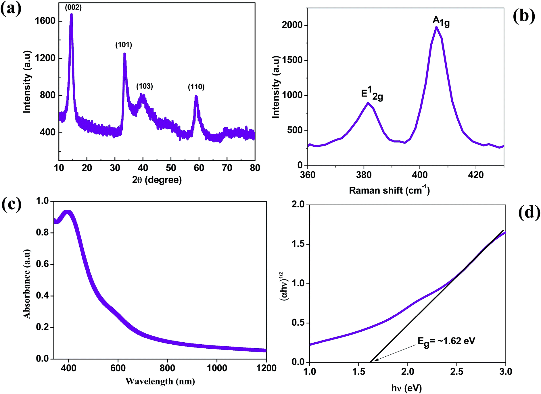 | ||
| Fig. 1 (a) X-ray diffraction pattern of MoS2. (b) Raman spectrum of MoS2. (c) Absorption spectrum and (d) Tauc plot of MoS2. | ||
To estimate the band gap of the as-synthesized MoS2 nanosheets, we measured the absorption spectra as shown in Fig. 1(c). The small noticeable peak at ∼600 nm corresponds to the spin–orbit split pair originating from the band edge excitonic transitions at the K point of the Brillouin zone.39 The broad peak at ∼395 nm corresponds to interband transitions from the occupied dz2 orbital to unoccupied dxy, dyz, dxz and dx2–y2 orbitals.40 From the absorption spectra, the calculated optical band gap is found to be ∼1.62 eV by using the Tauc plot with the allowed transitions for the MoS2 nanosheets.
Fig. S1 (a and b)† shows the typical scanning electron microscopy (SEM) images of the MoS2, indicating the nanosheet morphology of the as-synthesized material of few micrometers in length. High-resolution transmission electron microscopy (HR-TEM) was used for further analysis of MoS2 nanosheets. Fig. 2 (a–d) show the high-resolution TEM images of MoS2 nanosheets; all the TEM images suggest a nanosheet-like morphology, consistent with SEM images. The folded edges show parallel lines in Fig. 2(d), corresponding to different layers of MoS2 sheets with a d-spacing of ∼0.67 nm. The corresponding selected area electron diffraction (SAED) patterns shown in Fig. S2† indicate the crystalline nature of MoS2 nanosheets which supports the XRD and high-resolution TEM results. Further, energy dispersive X-ray analysis (EDAX) of MoS2 nanosheets was carried out. EDAX data are shown in ESI Fig. S3,† showing the stoichiometric ratios between Mo and S. Absorption spectra of oleic acid capped PbS quantum dots dispersed in toluene are shown in ESI Fig. S4.† The TEM images of PbS quantum dots are shown in Fig. S5,† indicating monodispersed QDs with an average size of ∼3.2 nm.
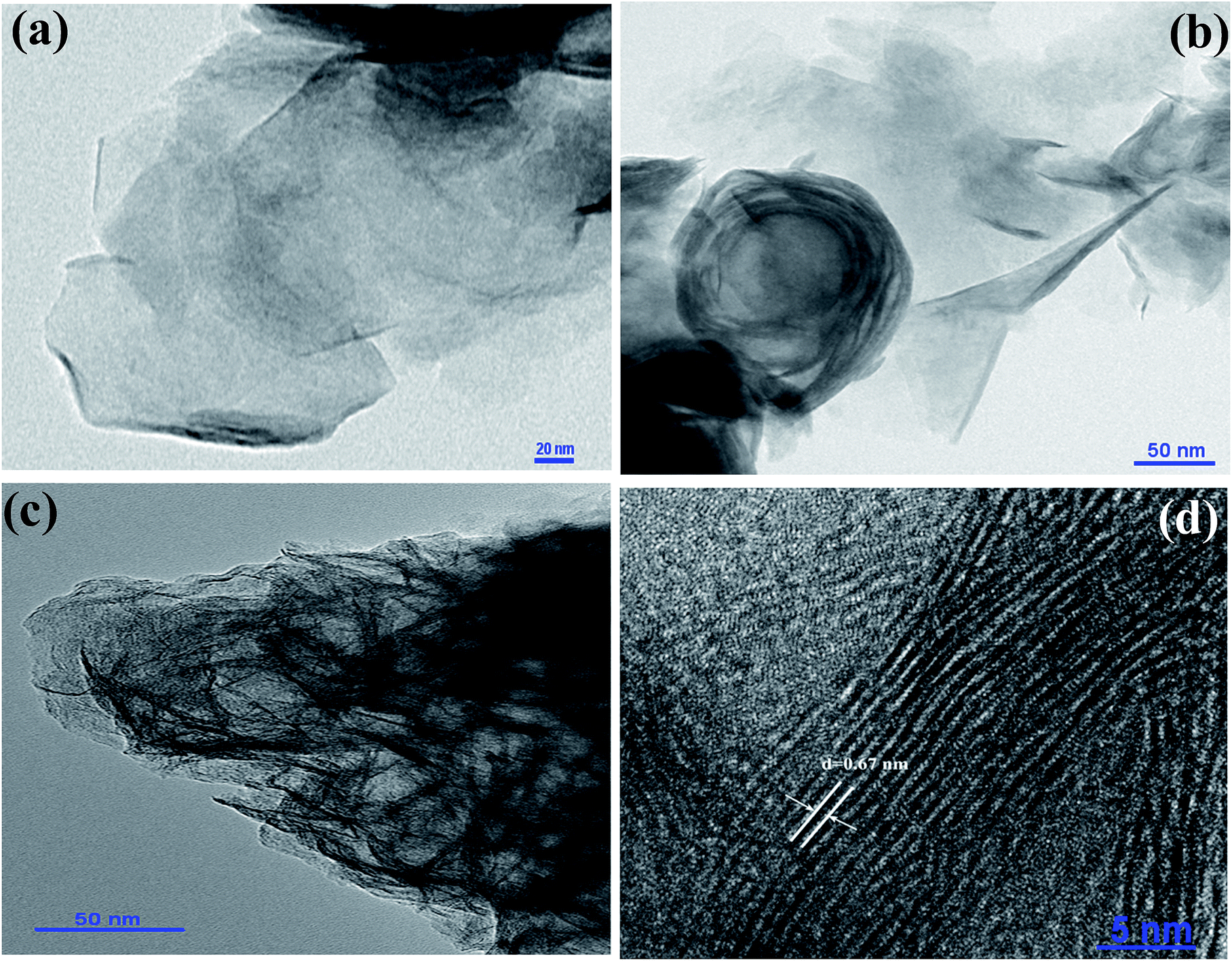 | ||
| Fig. 2 (a)–(d) show the TEM images of MoS2. d-Spacing between the MoS2 layers shown in figure (d) is 0.67 nm. | ||
Fig. 3(a) shows the contact mode atomic force microscopy (AFM) topography of a thin MoS2 nanosheet deposited on a Si substrate. We have used contact mode AFM to determine the thickness and to characterize the topography of the deposited sheets. The height profile obtained from the solid white line is shown in Fig. 3(b). It is noted that the height of the MoS2 nanosheet deposited on a Si substrate is found to be ∼10 nm. The as-synthesized MoS2 nanosheets are used as a hole transport layer to build PbS quantum dot solar cells. The solar cell device architecture is shown in Fig. 4(a) and the corresponding cross sectional SEM image is shown in Fig. 4(b). The typical I–V characteristics for devices with and without the MoS2 hole transport layer are shown in Fig. 4(c). The device without MoS2 shows a power conversion efficiency of 0.92%, with an open circuit voltage (Voc) of 0.46 V, a short circuit current density (Jsc) of 6.84 mA cm−2 and a fill factor of 30%. The insertion of MoS2 nanosheets as a hole transport layer improves the efficiency from 0.92% to 2.48% due to overall increments in Voc, Jsc and FF. The EQE results shown in Fig. 4(d) show higher photon to current conversion ratios for the entire wavelength range for the device with MoS2 nanosheets compared with the pristine device. The increase in EQE (%) and Jsc is attributed to superior charge collection in the latter case. The photovoltaic figures of merits of the photovoltaic devices are shown in Table 1. Fig. 5(a) shows the typical statistical variations in the efficiency of five solar cell devices. The enhancement in photovoltaic performance due to the insertion of the MoS2 layer is explained by the energy band diagram, shown in Fig. 5(b). In the absence of the MoS2 layer photo generated electrons and holes both are allowed to transfer to the Au electrode. This would enhance the photo carrier recombination at the PbS–Au interface and thereby reduce the current generation of the solar cells. Further, the 1.62 eV band gap of the MoS2 layer pushes its conduction band position well above the conduction band of PbS QDs, which blocks the transfer of electrons from PbS to the MoS2 layer. The selective extraction of holes at the PbS–MoS2 interface reduces the recombination of the photo generated carriers, thereby enhancing the current generation of the solar cells. Further, the hole carrier selectivity of the MoS2 layer reduces the voltage loss by reducing the Fermi energy pinning at the PbS–Au interface which helps to increase the voltage generation and fill factor of the solar cells.
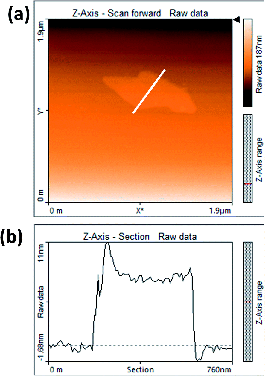 | ||
| Fig. 3 (a) AFM image of MoS2 nanosheets and (b) corresponding AFM height profile of MoS2 nanosheets. | ||
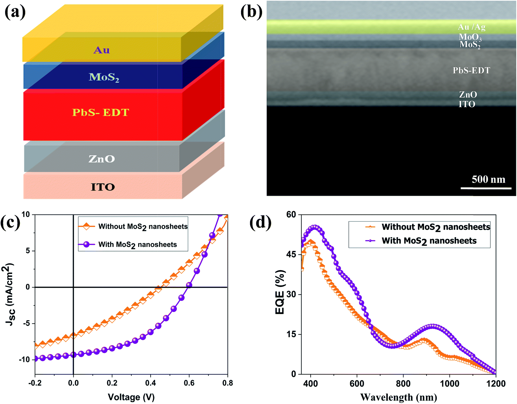 | ||
| Fig. 4 (a) Solar cell device architecture. (b) Cross sectional SEM image of the device. (c) The I–V characteristics of the solar cells. (d) External quantum efficiency (EQE) of the solar cells. | ||
| Device | V oc (V) | J sc (mA cm−2) | Fill factor | Efficiency (η%) |
|---|---|---|---|---|
| Without MoS2 | 0.46 | 6.84 | 0.30 | 0.92 |
| With MoS2 | 0.60 | 9.30 | 0.45 | 2.48 |
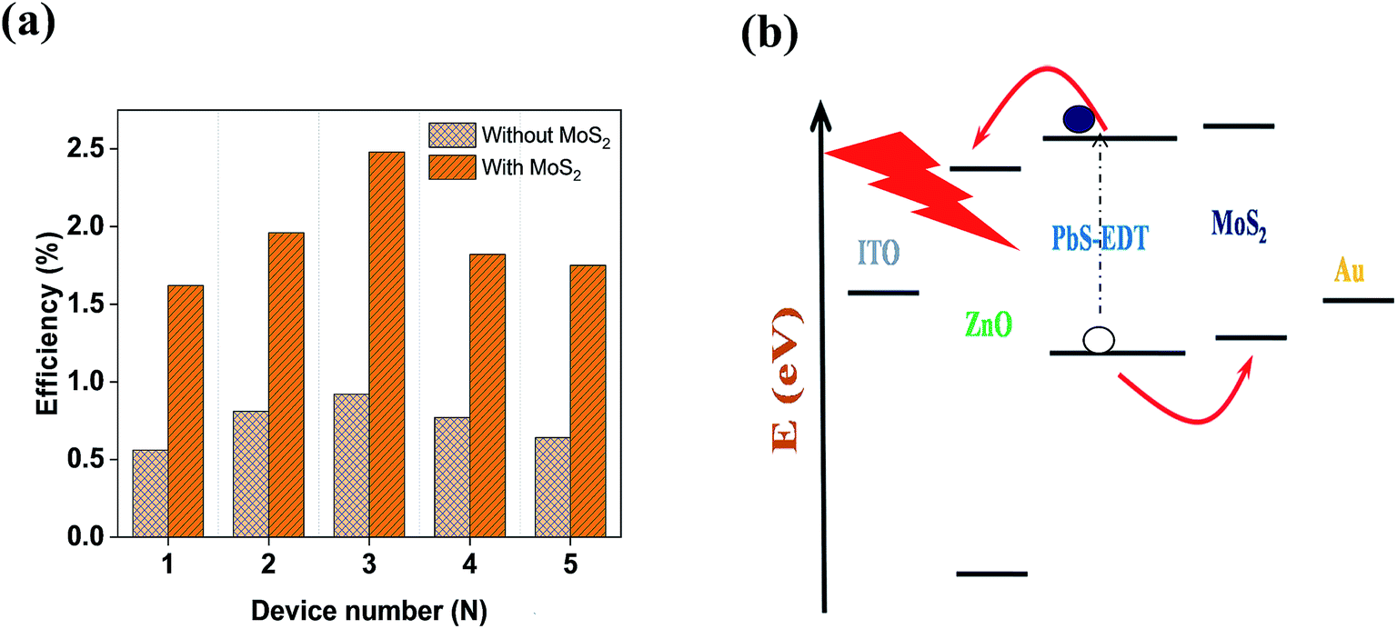 | ||
| Fig. 5 (a) Statistical variation of the solar cells. (b) Energy level diagram of a solar cell. | ||
4 Conclusions
In conclusion, we have demonstrated the matrix free deposition of 2D MoS2 nanosheets by the spin coating process. We have successfully developed a hole transport layer by using 2D MoS2 nanosheets, which improves the efficiency of PbS quantum dot solar cell devices from ∼0.92% to ∼2.48%. In solar cell devices it improves the charge extraction and reduces the carrier recombination. These improvements help to boost the efficiency of the solar cells by enhancing the short circuit current, open circuit voltage and fill factor. Our results open up new opportunities to use inorganic 2D MoS2 as an alternative to organic hole transporting materials for the development of the next generation solar cell devices.Conflicts of interest
All authors declare no conflicts of interest.Acknowledgements
We would like to thank the funding agencies SERB extramural funding, India (No: EMR/2015/002415), DST Nanomission, India (No: SR/NM/NT-1011/2105 (G)), and UGC SRF fellowship no. 2121251076. Dr D. J. Late would like to thank SERB for the SERB Research scientist grant.References
- I. B. Amara, E. B. Salem and S. Jaziri, Optoelectronic response and excitonic properties of monolayer MoS2, J. Appl. Phys., 2016, 120, 051707 CrossRef.
- Q. Xiang, J. Yu and M. Jaroniec, Synergetic Effect of MoS2 and Graphene as Cocatalysts for Enhanced Photocatalytic H2 Production Activity of TiO2 Nanoparticles, J. Am. Chem. Soc., 2012, 134, 6575–6578 CrossRef CAS PubMed.
- D. J. Late, B. Liu, H. S. S. R. Matte, V. P. Dravid and C. N. R. Rao, Hysteresis in Single-Layer MoS2 Field Effect Transistors, ACS Nano, 2012, 6, 5635–5641 CrossRef CAS PubMed.
- B. Radisavljevic, A. Radenovic, J. Brivio, V. Giacometti and A. Kis, Single-Layer MoS2 Transistors, Nat. Nanotechnol., 2011, 6, 147–150 CrossRef CAS PubMed.
- F. A. McGuire, Y. C. Lin, K. Price, G. B. Rayner, S. Khandelwal, S. Salahuddin and A. D. Franklin, Sustained Sub-60 mV/decade Switching via the Negative Capacitance Effect in MoS2 Transistors, Nano Lett., 2017, 17, 4801–4806 CrossRef CAS PubMed.
- W. Zhang, J. K. Huang, C. H. Chen, Y. H. Chang, Y. J. Cheng and L. J. Li, High-Gain Photo-transistors Based on a CVD MoS2 Monolayer, Adv. Mater., 2013, 25, 3456–3461 CrossRef CAS PubMed.
- D. S. Tsai, K. K. Liu, D. H. Lien, M. L. Tsai, C. F. Kang, C. A. Lin, L. J. Li and J. H. He, Few-Layer MoS2 with High Broadband Photogain and Fast Optical Switching for Use in Harsh Environments, ACS Nano, 2013, 7, 3905–3911 CrossRef CAS PubMed.
- K. P. Wang, Y. Y. Feng, C. X. Chang, J. X. Zhan, C. W. Wang, Q. Z. Zhao, J. N. Coleman, L. Zhang, W. J. Blau and J. Wang, Broadband Ultrafast Nonlinear Absorption and Nonlinear Refraction of Layered Molybdenum Dichalcogenide Semiconductors, Nanoscale, 2014, 6, 10530–10535 RSC.
- K. P. Wang, J. Wang, J. T. Fan, M. Lotya, A. O'Neill, D. Fox, Y. Y. Feng, X. Y. Zhang, B. X. Jiang, Q. Z. Zhao, H. Z. Zhang, J. N. Coleman, L. Zhang and W. J. Blau, Ultrafast Saturable Absorption of Two-Dimensional MoS2 Nanosheets, ACS Nano, 2013, 7, 9260−–9267 CrossRef CAS PubMed.
- W. Zhang, C. P. Chu, J. K. Huang, C. H. Chen, M. L. Tsai, Y. H. Chang, C. T. Liang, Y. Z. Chen, Y. L. Chueh and J. H. He, Ultrahigh-Gain Photodetectors Based on Atomically Thin Graphene MoS2 Heterostructures, Sci. Rep., 2014, 4, 3826 CrossRef PubMed.
- Q. H. Wang, K. K. Zadeh, A. Kis, J. N. Coleman and M. S. Strano, Electronics and Optoelectronics of Two-Dimensional Transition Metal Dichalcogenides, Nat. Nanotechnol., 2012, 7, 699–712 CrossRef CAS PubMed.
- J. Zhao, N. Li, H. Yu, Z. Wei, M. Liao, P. Chen, S. Wang, D. Shi, Q. Sun and G. Zhang, Highly Sensitive MoS2 Humidity Sensors Array for Noncontact Sensation, Adv. Mater., 2017, 29, 1702076 CrossRef PubMed.
- D. J. Late, Y. K. Huang, B. Liu, J. Acharya, S. N. Shirodkar, J. Luo, A. Yan, D. Charles, U. V. Waghmare, V. P. Dravid and C. N. R. Rao, Sensing Behavior of Atomically Thin-Layered MoS2 Transistors, ACS Nano, 2013, 7, 4879–4891 CrossRef CAS PubMed.
- S. Bertolazzi, D. Krasnozhon and A. Kis, Nonvolatile, Memory Cells Based on MoS2/Graphene Heterostructures, ACS Nano, 2013, 7, 3246–3252 CrossRef CAS PubMed.
- K. Roy, M. Padmanabhan, S. Goswami, T. P. Sai, G. Ramalingam, S. Raghavan and A. Ghosh, Graphene–MoS2 hybrid structures for multifunctional photoresponsive memory devices, Nat. Nanotechnol., 2013, 8, 826–830 CrossRef CAS PubMed.
- Y. Hou, A. B. Laursen, J. Zhang, G. Zhang, Y. Zhu, X. Wang, S. Dahl and I. Chorkendorff, Layered Nanojunctions for Hydrogen-Evolution Catalysis, Angew. Chem., Int. Ed., 2013, 52, 3621–3625 CrossRef CAS PubMed.
- H. Wang, Z. Lu, D. Kong, J. Sun, T. M. Hymel and Y. Cui, Electrochemical Tuning of MoS2 Nanoparticles on Three Dimensional Substrate for Efficient Hydrogen Evolution, ACS Nano, 2014, 8, 4940–4947 CrossRef CAS PubMed.
- Z. Wang and B. Mi, Environmental Applications of 2D Molybdenum Disulfide (MoS2) Nanosheets, Environ. Sci. Technol., 2017, 51, 8229–8244 CrossRef CAS PubMed.
- K. S. Novoselov, A. K. Geim, S. V. Morozov, D. Jiang, Y. Zhang, S. V. Dubonos, I. V. Grigorieva and A. A. Firsov, Electric Field Effect in Atomically Thin Carbon Films, Science, 2004, 306, 666–669 CrossRef CAS PubMed.
- R. Ganatra and Q. Zhang, Few-Layer MoS2: A Promising Layered Semiconductor, ACS Nano, 2014, 8, 4074–4099 CrossRef CAS PubMed.
- M. Shanmugam, C. A. Durcan and B. Yu, Layered Semiconductor Molybdenum Disulfide Nanomembrane Based Schottky-Barrier Solar Cells, Nanoscale, 2012, 4, 7399–7405 RSC.
- M. Shanmugam, T. Bansal, C. A. Durcan and B. Yu, Molybdenum Disulphide/Titanium Dioxide Nanocomposite-Poly 3-hexylthiophene Bulk Heterojunction Solar Cell, Appl. Phys. Lett., 2012, 100, 153901 CrossRef.
- X. Gu, W. Cui, H. Li, Z. Wu, Z. Zeng, S. T. Lee, H. Zhang and B. Sun, A Solution-Processed Hole Extraction Layer Made from Ultrathin MoS2 Nanosheets for Efficient Organic Solar Cells, Adv. Energy Mater., 2013, 3, 1262–1268 CrossRef CAS.
- M. Bernardi, M. Palummo and J. C. Grossman, Extraordinary Sunlight Absorption and One Nanometer Thick Photovoltaics Using Two-Dimensional Monolayer Materials, Nano Lett., 2013, 13, 3664–3670 CrossRef CAS PubMed.
- L. Y. Gan, Q. Zhang, Y. Cheng and U. Schwingenschlögl, Photovoltaic Heterojunctions of Fullerenes with MoS2 and WS2 Monolayers, J. Phys. Chem. Lett., 2014, 5, 1445–1449 CrossRef CAS PubMed.
- H. P. Wang, T. Y. Lin, C. W. Hsu, M. L. Tsai, C. H. Huang, W. R. Wei, M. Y. Huang, Y. J. Chien, P. C. Yang and C. W. Liu, Realizing High-Efficiency Omni directional n-Type Si Solar Cells via the Hierarchical Architecture Concept with Radial Junctions, ACS Nano, 2013, 7, 9325–9335 CrossRef CAS PubMed.
- H. P. Wang, T. Y. Lin, M. L. Tsai, W. C. Tu, M. Y. Huang, P. C. Yang, Y. J. Chien, C. W. Liu, Y. L. Chueh and J. H. He, Toward Efficient and Omnidirectional n-Type Si Solar Cells: Concurrent Improvement in Optical and Electrical Characteristics by Employing Microscale Hierarchical Structures, ACS Nano, 2014, 3, 2959–2969 CrossRef PubMed.
- S. H. Tsai, H. C. Chang, H. H. Wang, S. Y. Chen, C. A. Lin, S. A. Chen, Y. L. Chueh and J. H. He, Significant Efficiency Enhancement of Hybrid Solar Cells Using Core-Shell Nanowire Geometry for Energy Harvesting, ACS Nano, 2011, 5, 9501–9510 CrossRef CAS PubMed.
- W. R. Wei, M. L. Tsai, S. T. Ho, S. H. Tai, C. R. Ho, S. H. Tsai, C. W. Liu, R. J. Chung and J. H. He, Above-11%-Efficiency Organic-Inorganic Hybrid Solar Cells with Omnidirectional Harvesting Characteristics by Employing Hierarchical Photon-Trapping Structures, Nano Lett., 2013, 13, 3658–3663 CrossRef CAS PubMed.
- K. K. Liu, W. Zhang, Y. H. Lee, Y. C. Lin, M. T. Chang, C. Y. Su, C. S. Chang, H. Li, Y. Shi and H. Zhang, Growth of Large-Area and Highly Crystalline MoS2 Thin Layers on Insulating Substrates, Nano Lett., 2012, 12, 1538–1544 CrossRef CAS PubMed.
- Y. H. Lee, X. Q. Zhang, W. Zhang, M. T. Chang, C. T. Lin, K. D. Chang, Y. C. Yu, J. T. W. Wang, C. S. Chang and L. J. Li, Synthesis of Large-Area MoS2 Atomic Layers with Chemical Vapor Deposition, Adv. Mater., 2012, 24, 2320–2325 CrossRef CAS PubMed.
- Y. C. Lin, W. Zhang, J. K. Huang, K. K. Liu, Y. H. Lee, C. T. Liang, C. W. Chu and L. J. Li, Wafer-Scale MoS2 Thin Layers Prepared by MoO3 Sulfurization, Nanoscale, 2012, 4, 6637–6641 RSC.
- K. Chang and W. X. Chen, l-Cysteine-Assisted Synthesis of Layered MoS2/Graphene Composites with Excellent Electrochemical Performances for Lithium Ion Batteries, ACS Nano, 2011, 5, 4720 CrossRef CAS PubMed.
- M. A. Hines and G. D. Scholes, Colloidal PbS Nanocrystals with Size Tunable Near Infrared Emission: Observation of Post Synthesis Self Narrowing of the Particle Size Distribution, Adv. Mater., 2003, 15, 1844–1849 CrossRef CAS.
- L. K. Jagadamma, M. Abdelsamie, A. E. Labban, E. Aresu, G. O. N. Ndjawa, D. H. Anjum, D. Cha, P. M. Beaujuge and A. Amassian, Efficient inverted bulk-heterojunction solar cells from low-temperature processing of amorphous ZnO buffer layers, J. Mater. Chem. A, 2014, 2, 13321–13331 RSC.
- C. H. Chuang, P. R. Brown, V. Bulovic and M. G. Bawendi, Improved performance and stability in quantum dot solar cells through band alignment engineering, Nat. Mater., 2014, 13, 796–801 CrossRef CAS PubMed.
- D. J. Late, B. Liu, H. S. S. R. Matte, C. N. R. Rao and V. P. Dravid, Rapid Characterization of Ultrathin Layers of Chalcogenides on SiO2/Si Substrates, Adv. Funct. Mater., 2012, 22, 1894–1905 CrossRef CAS.
- M. Thripuranthaka, R. V. Kashid, C. S. Rout and D. J. Late, Temperature-dependent Raman spectroscopy of chemically derived few-layer MoS2 and WS2 nanosheets, Appl. Phys. Lett., 2014, 104, 081911 CrossRef.
- R. Coehoorn, C. Haas, J. Dijkstra and C. J. F. Flipse, Electronic-Structure of MoSe2, MoS2, and WSe2. I. Band-Structure Calculations and Photoelectron spectroscopy, Phys. Rev. B: Condens. Matter Mater. Phys., 1987, 35, 6195–6202 CrossRef CAS.
- L. A. King, W. Zhao, M. Chhowalla, D. J. Riley and G. Eda, Photo-electrochemical Properties of Chemically Exfoliated MoS2, J. Mater. Chem. A, 2013, 1, 8935–8941 RSC.
Footnote |
| † Electronic supplementary information (ESI) available. See DOI: 10.1039/c8na00272j |
| This journal is © The Royal Society of Chemistry 2019 |