
 Open Access Article
 This Open Access Article is licensed under a Creative Commons Attribution-Non Commercial 3.0 Unported Licence
Fingerprints of native defects in monolayer PbTe
C. E. Ekuma
U.S. Army Research Laboratory, Aberdeen Proving Ground, MD 21005-5069, USA. E-mail: cekuma1@gmail.com
First published on 29th October 2018
Abstract
Understanding the intricate interplay of defects and electron–electron interactions is crucial to exploiting the full potential of materials for practical applications. At the nanoscale, the combined effects are more pronounced due to quantum confinement and can have both positive and negative subtle effects on device performance. Herein, we report optoelectronic properties of pristine and disordered monolayer PbTe. We obtain the pristine electronic structure from first-principles calculations with the modified Becke–Johnson potential. We study the combined impact of random defects due to Te and Pb vacancies and material-specific electron–electron interactions on the electronic and optical properties of monolayer PbTe. We use a generalized energy-dependent Anderson–Hubbard Hamiltonian within a first-principles-based many-body typical medium method to self-consistently calculate the single-particle electronic structure. The absorption spectra, which also accounted for the effects of electron–hole interactions, are studied using valence electron energy-loss spectroscopy (VEELS) and they are obtained by solving the Bethe–Salpeter equation. Our results show an anomalous dependence on spin–orbit coupling for the pristine nanostructure and demonstrate that increased vacancy concentrations lead to, among other things, enhancement of the band gap, resonant shallow impurities, strong renormalization of the VEELS, and a systematic increase of the effective plasmon energy.
PbTe is a prototype lead salt semiconductor that has been actively studied for use in thermoelectric energy conversion devices and other optoelectronic applications.1–16 PbTe is one of the most studied and efficient thermoelectric materials for mid-temperature power generation. The thermoelectric performance, characterized by the figure of merit zT = σS2T/κ (σ is electrical conductivity, S is the Seebeck coefficient, and κ is thermal conductivity), depends on the carrier density (doping) and temperature T.4 In order to maximize the thermoelectric performance, the carrier density could be tuned by adjusting the dopant/defect concentrations, which also determines where the maximum of zT will be located in the temperature space.7 Therefore, obtaining high zT requires optimization of the doping level.4,7
Many techniques, both experimental and computational have been developed to probe the electronic structure of materials. One of the emerging techniques for characterizing changes in the electronic structure of materials is electron energy-loss spectroscopy (EELS) L(ω).17–22 EELS provides a non-optical approach for probing the electronic structure of materials. Recently, EELS has been used to study valence electron excitations in low-dimensional materials.23–27 Most EELS studies have focused mainly on ionization edges, which are edge loss energies corresponding to the excitation of core electrons generally above 100 eV.22,28–31 The features of the spectra in this regime are mainly due to the variations in the density of unoccupied states above the Fermi level.
In contrast, the low-loss spectra (valence EELS), which appear at lower energies below ≈50 eV, are less studied. Valence EELS (VEELS) reflects (i) the collective excitation of the valence states (plasmons) due to a singly excited valence electron in the unoccupied state in the conduction band, (ii) the low-energy interband transition of a single electron, and (iii) possible metastable excitons. VEELS could be most useful for characterizing disordered materials since the collective oscillation of the valence electrons and their energies (plasmon losses) is related to the density of the valence electrons. In particular, the electronic response of the material due to plasmon loss is a signature of the complex dielectric function, which is related to the experimental single scattering distribution through L(ω).22,25 As such, it is a natural quantity for characterizing the electronic properties of a material.22,28,29
Defects have been shown to be ubiquitous in materials, and at the nanoscale the impact is more pronounced due to quantum effects (see, e.g., ref. 32–34). This could have a significant impact on device performance. Herein, we have chosen PbTe, a well-known group IV–VI semiconductor used in thermoelectric energy conversion devices, and its alloy, a major component in the synthesis of optoelectronic systems for this study. Generally, defects can be in different forms.1,3,15 Depending on the growth conditions, both hole and electron conductivity have been observed in the bulk crystal of PbTe.1,3,35 The origin of free carriers, i.e., electron (hole) conductivity, is by now generally agreed to originate from Te (Pb) vacancies in bulk PbTe.1,3 Motivated in part by the recent experiments on lead salt nanocrystals confirming this observation, we explore the role of native defects due to Te and Pb vacancies in monolayer PbTe. While theoretical studies of Pb and Te vacancies have been reported at the DFT-level in the bulk crystal (see, e.g., ref. 8, 15 and 36) we are not aware of such a study for the monolayer crystal. This is not to say that the understanding of the pristine structure is not important as well. In our monolayer PbTe example [the crystal structure is shown in Fig. 1(a)], a rigorous study of the optoelectronic properties of the pristine structure is still lacking. As a result of this study, we will understand the main features of the electronic structure. However, to support the development of any practical applications, we also need to develop a better understanding of the properties of disordered PbTe. Herein, we use first-principles-based calculations to study the pristine structure and the defect morphology of disordered monolayer PbTe.
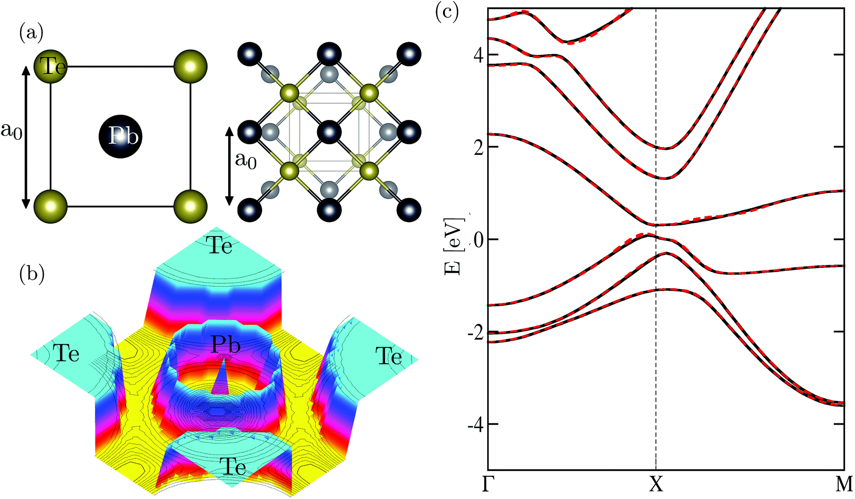 | ||
| Fig. 1 (a) Top and perspective view of the atomic structure of monolayer PbTe. The lattice exhibits a D4h (space group no. 123) tetragonal crystal structure. (b) The electron localization function of monolayer PbTe. (c) The density functional theory band structure (black dashed bands) reproduced by the downfolded Hamiltonian H0 (solid red bands) within the energy window [–10.0, 12.0] eV obtained using the mBJ functional. A direct band gap Eg ≈ 0.28 eV around the X-point of the k-space is predicted. | ||
A significant challenge is that defects and electron–electron interactions are of central importance to understanding many physical and chemical processes in nanomaterials including photoemission, cation exchange, and accommodation of off-stoichiometry. Modeling the interplay of defects and electron–electron interactions is very challenging and computational approaches are still not yet well-developed. The lack of first-principles-based many-body calculations of the effects of defects on the properties of monolayer PbTe is one of the motivations of this study.
The basic features of the electronic structure of the bulk crystal are known both experimentally and theoretically (see above, and also, e.g., ref. 37–41). However, there are few computational results on the properties of monolayer PbTe (see, e.g., ref. 13 and 42) and none to the best of our knowledge on the role of defects or impurities. Experimentally, we are not aware of any reported results on the properties of disordered monolayer PbTe. Hence, our first-principles data could aid in the experimental design and fabrication of single-crystals of the lead salt family for optoelectronic applications that could benefit from the flexibility that abounds in nanostructures.
The purpose of this paper is threefold. First, we investigate the electronic properties of pristine PbTe as obtained from modern electronic structure calculations based on the modified Becke–Johnson (mBJ) potential.43 The mBJ potential yields the band gap and related properties of materials in better agreement with the experiment.4,16 Second, we study the role of native defects due to randomly distributed Te and Pb vacancies and material-specific electron–electron interactions in the electronic and absorption spectra of monolayer PbTe. Instead of the supercell approach of the density functional theory, which could be prohibitively expensive to simulate low vacancy concentrations ∼1% and only describes ordered defect structures, we used the recently developed first-principles-based typical medium dynamical cluster approximation (TMDCA).44,45 The TMDCA systematically takes into account the intrinsic random nature of the defect states in crystals.44,46 As noted above, electron–electron interactions could be important to understanding the electronic and absorption features of monolayer PbTe. To adequately account for these many-body fine structures, we used the recently formulated energy-dependent Anderson–Hubbard Hamiltonian.45 This energy-dependent Hamiltonian uses a dynamical material-specific screened Coulomb interaction W(E) obtained by solving a separate self-consistent, quasiparticle Green's function and screened Coulomb (sqGW) calculations instead of the usual onsite Hubbard interactions parameter.45 We characterize the electronic structure using the quasiparticle self-energy ∑(E) obtained from our self-consistent TMDCA calculations. Third, we explore and provide the absorption spectra of disordered monolayer PbTe via valence electron energy-loss spectroscopy. The absorption spectra accounted for the effects of electron–hole interactions by solving the Bethe–Salpeter equation (BSE) in the particle–hole channel as described in ref. 45 and 47. The BSE calculation used the single-particle Green's function from our self-consistent TMDCA results, which accounts for the effects of both native defects due to vacancies and electron–electron interactions. We hope that the presented approach and results will motivate its use in characterizing the properties of PbTe and materials in general. Also, it is our hope that it stimulates future experiments to investigate the pristine crystals of monolayer PbTe and the role of defects on both the electronic properties and absorption spectra, especially the VEELS. Understanding the VEELS could be crucial since the states around the Fermi level are the most important in determining the electronic, optical, and transport properties of materials.
The main findings of our work are the following: (1) pristine monolayer PbTe is a semiconductor with a direct narrow band gap of ∼0.28 eV occurring around the X-point of the k-space. The band extrema around the Fermi level are slightly shifted away from the X-point due to band inversion. The electronic structure exhibits anomalous behavior due to spin–orbit coupling (SOC), which increases rather than decreases the band gap. (2) Te and Pb vacancies in monolayer PbTe are found to have significantly different effects. Specifically, while Pb vacancies lead to more scattering and the generation of impurity levels close to the band edge, Te vacancies lead to increased band gap renormalization. In both cases, the defect-induced levels are mainly shallow impurity states. That is, the impurity states are located outside the band gap, and can be characterized as virtual bound states residing within the bands as resonant states. From this characterization, disordered PbTe single-crystals could be observed to be defect-tolerant. The ability of monolayer PbTe to host impurity states as shallow levels without the formation of localized deep-levels could be central to unraveling the unusual properties of the family of lead salts for diverse applications, e.g., as thermoelectric materials. (3) The intricate interplay of defects and electron–electron interactions affect the absorption spectra in a subtle way. In particular, we find that many-body effects are essential for the proper description of the VEELS, e.g., the plasmon energy is ∼40% higher when electron–electron interactions are neglected.
To study the interplay of random native defects and material-specific screened Coulomb interactions, we use the energy-dependent Anderson–Hubbard Hamiltonian45
 | (1) |
The Hamiltonian for the pristine crystal Ĥ0 and W(E) are obtained from self-consistent calculations based on the density functional theory (DFT)48 and the GW method,49 respectively. For the monolayer PbTe, we initially carried out full structural (ionic positions and cell volume) relaxation using the linearized augmented planewave (LAPW) method with the Perdew–Burke–Ernzerhof (PBE)50 exchange-correlation functional. The calculated lattice parameters are a0 = 4.49 Å and c = 23.30 Å. The out of plane lattice constant c separates periodic images of monolayer PbTe to avoid the artifacts of the periodic boundary condition. Using the optimized crystal lattice, we carried out self-consistent electronic structure calculations with the modified Becke–Johnson potential43 as implemented in WIEN2K.51 This latter calculation yields the Kohn–Sham eigenvalues and eigenfunctions. All the DFT calculations were performed relativistically including spin–orbit coupling using a well-converged basis set with a dense Brillouin zone sampling grid of 20 × 20 × 1, a LAPW sphere radius of 2.50 Bohr for Pb and Te, and an RminKmax = 9, where Rmin is the smallest sphere radius in the system and Kmax is the plane wave momentum cutoff. We obtained Ĥ0 from the Kohn–Sham eigenvalues and eigenfunctions using a downfolding method that transforms the basis to a set of maximally localized Wannier functions as implemented in WANNIER90.52 For the monolayer PbTe considered herein, Ĥ0 includes Pb (s, p, and d orbitals) and Te (s, p, and d orbitals) within the energy window [−10.0, 12.0] eV. In essence, only the f-electrons, which are deep in energy are neglected in Ĥ0. The 36-bands that make up Ĥ0 reproduce the DFT band structure, with a direct single-particle energy band gap Eg ≈ 0.28 eV around the X-point of the k-space [Fig. 1(c)]. To obtain W(E), we performed sqGW calculations using an energy cutoff of 450 (160) eV for the DFT (sqGW) with a 9 × 9 × 1 Γ-centered grid to represent the reciprocal space as implemented in the Vienna Ab Initio Simulation Package.53
The single-particle Green's function is a vital quantity that could be used to obtain the electronic and related properties of materials. For an infinite disordered crystal, only an approximate single-particle Green's function could be obtained in our case, based on the typical medium dynamical cluster approximation. The TMDCA self-consistency is based on an approach consistent with the dynamical cluster theory approaches to correlated electron systems.54,55 The TMDCA maps the lattice problem (1) onto a periodically repeated system of size Nc primitive cells embedded in a typical medium.44,46 We solve iteratively the TMDCA equations in the presence of both random Te and Pb vacancies and W(E) to obtain the typical single-particle Green's function. Details of the implementation of the first-principles TMDCA are presented in ref. 44.
In order to calculate the valence-loss spectra, we need to obtain the two-particle Green's function. To achieve this, the single-particle Green's functions obtained from the TMDCA self-consistent calculations are used to solve the Bethe–Salpeter equation (BSE). Details of the implementation of the BSE for disordered materials are presented in ref. 45 and 47. For brevity, we will present only the essential steps to calculate the valence-loss spectra from the BSE. After obtaining the disorder and electron–electron interaction dressed single-particle Green's function from the TMDCA self-consistent calculations, we calculate the dynamical charge susceptibility, which accounted for the screening within the typical medium as χ(![[q with combining right harpoon above (vector)]](https://www.rsc.org/images/entities/i_char_0071_20d1.gif) , ω) = χ0(, ω)[
, ω) = χ0(, ω)[ − W(ω)χ0(, ω)]−1, where χ0 is the bare charge susceptibility obtained as the convolution of two single-particle Green's functions, W(ω) is the material-specific dynamical screened Coulomb interaction, ω is the excitation energy, and 1 is the identity matrix.45,47 Recall that the dynamical dielectric function ε(, ω) ∝ χ(, ω). Then, we obtain the valence-loss function (for → 0)
  .
.
Imperfections in materials could take many forms not limited to antisites, adatoms, and vacancies. In the present study, we focus on material imperfections due to Te and Pb vacancies, respectively. We model the vacancies with a bimodal site potential Viσα = Vi∈{0, Wb} randomly generated using the probability mass functions P(Vi = W) = δ and P(Vi = W) = 0, where 0 (W) is for the ordered (disordered) site. The vacancy potential is set to an energy far greater than the pristine bandwidth of monolayer PbTe. All the TMDCA calculations used a tetragonal crystal structure on a dense Brillouin zone sampling grid of 20 × 20 × 1 ![[k with combining right harpoon above (vector)]](https://www.rsc.org/images/entities/i_char_006b_20d1.gif) points.
points.
We start the discussion of our results with the electronic properties of the pristine structure. We show in Fig. 1(a) the optimized atomic structure of monolayer PbTe, which contains 1-Pb and 1-Te in the unit cell forming a square lattice positioned in the mirror plane z = 0. We predict a lattice constant a0 ∼ 4.48 Å. In Fig. 1(b), we present the electron localization function, which shows mixed ionic-covalent bonding further confirmed by the sum of the bond order ∼2.22 (2.34) for Pb (Te) as obtained from the net atomic charges.56 We present in Fig. 1(c) the calculated band structure of monolayer PbTe. The calculated spectra share some qualitative similarities with those previously reported, but important quantitative differences exist, which are due to our use of the mBJ functional. For instance, we predict a direct band gap Eg ∼ 0.28 eV around the X-point of the high symmetry zone. We are not aware of any reported experimental band gap of monolayer PbTe and hence we cannot compare our predicted band gap with experimental ones. We note that the PBE-DFT band gaps with and without SOC are 0.19 and 0.24 eV, respectively. Recent DFT calculations indicated a near metallic solution with a band gap of ∼ 0.09 eV.57 The data of Liu et al.58 and Kobayashi42 led to band gaps of 0.26 and 0.16 eV, respectively. We checked the dependence of the band gap on both lattice and computational parameters such as energy cutoff, Brillouin zone sampling, and radii of the LAPW spheres. In both cases, we noticed a band gap change of ∼±40 meV. Specifically, we found that a compression or expansion (∼±2%) of the lattice parameters could induce a band gap change of up to ±50 meV. This observation mirrors the anomalous dependence of the energy band gap on pressure observed in bulk lead salts.4 The pressure-induced effect in the energy band gap was attributed to the band ordering of the states around the Fermi level, which depends on the spin–orbit coupling.39,41 The predicted band gap is smaller than its bulk counterpart Eg ∼ 0.36 eV by more than 20%. The smaller band gap of the monolayer could be understood from the above-described scenario since the predicted lattice constant of the monolayer crystal (∼4.48 Å) is smaller than the bulk lattice constant of ∼6.46 Å. We also note recent first-principles calculations of IV–VI nanostructures, which attributed this anomalous behavior to pressure and crystal field effects.58,59 As a function of the input parameters, we noticed that using a smaller k-point grid, e.g., 8 × 8 × 1 to sample the Brillouin zone increases the band gap by as much as 40 meV. In a conventional semiconductor, SOC generally leads to the decrease of the band gap. Surprisingly, our data show that SOC has anomalous effects on the electronic structure as it increased the band gap by as much as ∼95 meV. We ascribe this behavior to the pressure-induced topological insulator (TI) in monolayer PbTe.60 The significance of this is that since the TI phase is intrinsic and has such a large band gap, it could be stable at room temperature with significantly smaller finite size effects.61
Remarkably, the band structure of the monolayer shares many commonalities with the bulk counterpart, especially around the Fermi level. From Fig. 1(c), the Fermi level is located around the X-point, which also hosts the valence band maximum and the conduction band minimum. The bands are derived from a strong hybridization between Pb 6p (mainly in the conduction bands) and Te 5p (mainly in the valence bands) states with some contribution primarily from the s and d states at higher energies of Pb and Te, respectively. In the conduction band, the spin–orbit splitting (SOS) of the two low-lying states at the Γ-point is ∼1.54 eV and ∼0.22 eV at the X-point. The conduction band SOS defined by the splitting of the second and third low-lying conduction bands at the Γ-point is ∼0.60 eV. In the valence states, the SOS of the low-lying states is ∼0.30 eV and ∼1.0 eV at the X- and Γ-points, respectively. The calculated SOS values compare rather well with the bulk ones from both first-principles calculations and experiments.4,62,63
In order to study the effects of electron–electron interactions and native defects on the electronic properties of monolayer PbTe, we computed the quasiparticle self-energy ∑(E). The self-energy could be said to be the “memory function” of a material as it is a measure of the energy acquired by carriers due to changes in their local environment. It is an important fingerprint of the electronic and related properties of materials. For example, ∑(E) is directly related to the scattering rate and the mass enhancement factor.64 The self-energy is obtained from the single-particle Green's function as  , where
  and G are the site-excluded and fully (disorder and electron–electron interactions) dressed Green's functions, respectively.
We show in Fig. 2 and 3 the imaginary part of the quasiparticle self-energy calculated at various Te and Pb vacancy concentrations. For small δ, strong resonance states are observed around the Fermi level, especially at the conduction band minimum, which is mainly due to Pb-pz states. As δ increases, we observed resonant state broadening and significant spectra weight redistribution and transfer to higher energies. It can be observed from Fig. 2 and 3 that the band gap is systematically enhanced as it increases with increasing δ. This effect is more pronounced in the data for disorder due to Te vacancies (Fig. 2). Also, Pb vacancies seem to induce more scattering in the spectra as could be seen from the higher spikiness (Fig. 3). Surprisingly, for all the vacancy concentrations considered herein, the defect-induced states are all shallow impurity levels residing in the bands as resonant states. This observation suggests that monolayer PbTe could be a potential defect-tolerant material.65,66 A similar observation was recently reported for monolayer PbSe.59 Hence, the ability of PbTe to host defect states as shallow levels outside the band gap could be a generic property of the family of lead salts, which warrants further investigation. The observed defect tolerance offers an opportunity for exploring monolayer PbTe as a candidate for application in intermediate solar cell devices and could be used to optimize its application as a thermoelectric material.
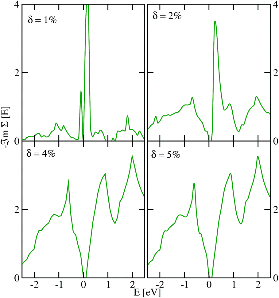 | ||
| Fig. 2 The TMDCA@DFT results for the imaginary part of the quasiparticle self-energy of monolayer PbTe at various Te vacancy concentrations δ. The Fermi level is set at zero of the energy scale. | ||
 | ||
| Fig. 3 The TMDCA@DFT results for the imaginary part of the quasiparticle self-energy of monolayer PbTe at various Pb vacancy concentrations δ. The Fermi level is set at zero of the energy scale. | ||
One significant implication of the TMDCA approach is that it uses the same primitive crystals of the pristine material to study the disordered crystals. This has advantages as well as disadvantages. While it allows for the study of very low concentrations since the computational cost does not scale with the system size as in the DFT supercell method, it, however, neglects any structural relaxation around the vacant sites. To ascertain the latter effect, we performed relaxed supercell calculations of size 5 × 5 × 1 corresponding to a 4.0% Te and Pb vacancy concentration, respectively, using PBE-DFT. As can be seen from Fig. 4, both the DFT and the TMDCA data are qualitatively similar, especially at low energy. Subtle differences could be attributed to the different sampling techniques used in the two approaches: random disorder sampling used in the TMDCA and no sampling since defects are ordered in DFT. Hence, the neglect of lattice relaxation has insignificant effects on the conclusions reached in our analysis. These data also support the observed defect tolerance since no deep-levels are induced within the band gap.
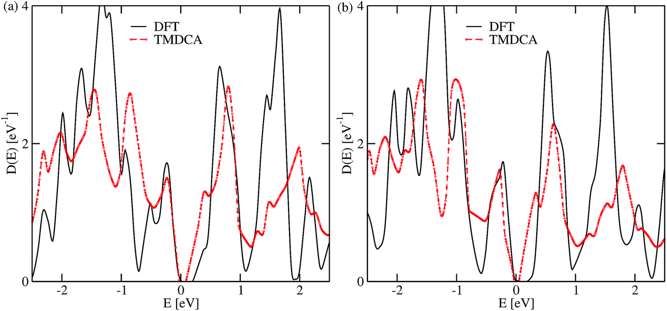 | ||
| Fig. 4 Comparison of the density of states obtained using the DFT supercell approach with the TMDCA@DFT for Te (a) and Pb (b) vacancy concentrations δ = 4.0%. The DFT calculations used a 5 × 5 × 1 supercell with the PBE functional and the TMDCA@DFT used a normal averaging procedure. Observe that in both cases studied herein, the defect-induced states are all resonant levels with no localized deep-level states within the band gap. | ||
To gain some insight into the absorption spectra of disordered monolayer PbTe, we show in Fig. 5 and 6 the VEELS calculated at various Te and Pb vacancy concentrations, respectively. We note that the computed spectra show more features than traditional absorption spectra due to the smaller broadening ∼10−3 eV used in our calculations. As could be seen, there are several features of the spectra. The pristine VEELS show rather sharp plasmon peaks. Noticeable additional peaks and features are also observed, which we attribute to multiple plasmon losses. This behavior is reminiscent of what is observed in simple metals and most semiconductors but not in transition metal oxides that show single broad plasmon spectra.21,22 The prominent feature of the spectra is the main plasmon peak at ∼3.66 eV. The pristine spectra show two sharp peaks at ∼1.10 and 1.85 eV. These lower fine structures are followed by a shoulder at 2.58 eV, two other peaks at 3.13 and 4.30 eV, another shoulder at ∼5.0 eV, and several other fine structures at higher energies. We could attribute the characteristic of the prominent low energy excitations to the dipole allowed transition from Te-p states located below the Fermi level to available unoccupied states above the Fermi level.
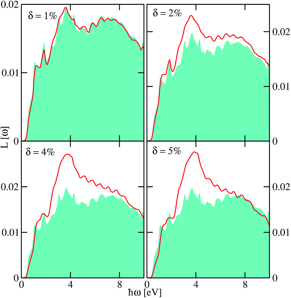 | ||
| Fig. 5 The low-energy loss spectra of monolayer PbTe at various Te vacancy concentrations δ as a function of the excitation energy ℏω. The spectra included the effects of electron–hole interactions through the Bethe–Salpeter equation. For reference, we also include the spectra of pristine monolayer PbTe depicted with a turquoise background. | ||
 | ||
| Fig. 6 The low-energy loss spectra of monolayer PbTe at various Pb vacancy concentrations δ as a function of the excitation energy ℏω. The spectra included the effects of electron–hole interactions through the Bethe–Salpeter equation. For reference, we also include the spectra of pristine monolayer PbTe depicted with a turquoise background. | ||
The impact of the Te and Pb vacancies on the overall magnitude of L(ω) varies at different parts of the spectra. While the obtained disordered spectra due to Te and Pb vacancies share some commonalities, some subtle differences could be seen as highlighted below. In both cases, the L(ω) appears to be slightly blue shifted. At higher energies above ∼2.12 eV, we observed an increase in the magnitude of L(ω) as the vacancy concentration increases. This could be attributed to the reduction in the generation of free excitons as disorder induced by the vacancies enhances the localization of carriers in the proximity of the Fermi level. However, below ∼2.12 eV, the magnitude of L(ω) initially increased, then decreased at δ ∼ 4% before increasing monotonically as δ is increased. The decreased valence-loss at δ ∼ 4% signifies increased absorption, which could be within the optimal doping concentration in monolayer PbTe. This could be further explored to harness its optoelectronic properties. Also, as δ is increased, some of the fine structures observed in the pristine spectra get broadened and then disappear. For example, the sharp features at ∼(1.10 and 1.85) eV are systematically broadened as δ increases and could be seen to merged into a shoulder at ∼1.88 eV for δ ∼ 5%. As observed further from Fig. 6, that as the Pb vacancy concentration is increased, impurity states appear at the band edge, which are blue-shifted as δ is increased and a shoulder could be observed at ∼2.0 eV. These two spectral features are absent in the data obtained for the disorder due to Te vacancies (Fig. 5). The former feature is predominantly due to Pb-pz states while the latter emanated mainly from a hybridization between the Pb-px and Pb-py states.
The subtle additional fine structures below and above the prominent peak of the spectra observed both in the pristine and disordered crystal could be due to additional energy loss from nondipole transitions and collective excitation. This could occur since we obtained the valence-loss spectra using the BSE, which takes into account higher order diagrams beyond the random-phase approximation. We note that the RPA data (not shown) show fewer or no structures within this photon-energy range. Consider the electron energy loss associated with a single electron transition 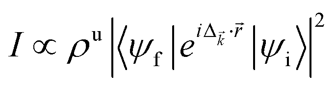 ,67 where ρu is the unoccupied density of states, ψi (ψf) is the occupied initial (unoccupied final) state, Δ is the momentum transfer from the incident electron to the excited electron, and
 ![[r with combining right harpoon above (vector)]](https://www.rsc.org/images/entities/i_char_0072_20d1.gif) is the relative position of the electron. Within the RPA, the dipole approximation I ≈ |〈ψf|iΔ·|ψi〉|2 is used, which guarantees that all the observed transitions obey the dipole selection rule change of the angular momentum quantum number Δl = ±1. However, due to the proximity of the outer shell electrons to the Fermi level, Δ· could approach or even exceed unity rendering the dipole approximation inapplicable. Even more importantly, our calculated spectra also included the effects of both electron–electron and electron–hole interactions. The latter two effects and the higher order diagrams accounted for in the BSE account for crystal local-field effects due to inhomogeneities of the electronic density that could be missed in dipole approximations. The crystal local-field effects have been shown to have significant effects on the absorption spectra and hence the plasmon features in some materials.68,69 Our recent sqGW calculations show that crystal local-field effects significantly affect the optical properties of monolayer MoS2, e.g., the quasiparticle band gap is reduced by ∼8.0%.45
is the relative position of the electron. Within the RPA, the dipole approximation I ≈ |〈ψf|iΔ·|ψi〉|2 is used, which guarantees that all the observed transitions obey the dipole selection rule change of the angular momentum quantum number Δl = ±1. However, due to the proximity of the outer shell electrons to the Fermi level, Δ· could approach or even exceed unity rendering the dipole approximation inapplicable. Even more importantly, our calculated spectra also included the effects of both electron–electron and electron–hole interactions. The latter two effects and the higher order diagrams accounted for in the BSE account for crystal local-field effects due to inhomogeneities of the electronic density that could be missed in dipole approximations. The crystal local-field effects have been shown to have significant effects on the absorption spectra and hence the plasmon features in some materials.68,69 Our recent sqGW calculations show that crystal local-field effects significantly affect the optical properties of monolayer MoS2, e.g., the quasiparticle band gap is reduced by ∼8.0%.45
To further quantify the VEELS, we calculate the effective plasmon energy Epc of monolayer PbTe at various Te and Pb vacancy concentrations, respectively. This could be obtained as the maximum of the VEELS70,71 from Fig. 5 and 6. The Drude model could also be used to approximate the effective plasmon energy as EDp= ℏωp,72 where ℏ is the reduced Planck constant and ωp is the plasmon frequency, which we approximate as ωp = ∫ωε2(ω)dω for a given δ. We show in Table 1 the Ep from the two approaches at various δ. As expected, the effective plasmon energy estimated from the Drude model decreases as the vacancy concentration is increased due to a decrease in valence electron density. However, the effective plasmon energy obtained using the peaks of the VEELS increases with increasing vacancy concentrations due to many-body effects, which renormalized the spectra, especially the valence electron density.
| δ | E p c [Te] | E p c [Pb] | E D p [Te] | E D p [Pb] |
|---|---|---|---|---|
| 0.0 | 3.67 (6.27) | 3.67 (6.27) | 4.96 | 4.96 |
| 1.0 | 3.59 | 3.55 | 5.09 | 4.74 |
| 2.0 | 3.60 | 3.56 | 4.59 | 4.30 |
| 4.0 | 3.78 | 3.60 | 4.41 | 3.89 |
| 5.0 | 3.87 | 3.69 | 4.20 | 3.81 |
We also observe that the Drude model significantly overestimates (at low δ) and underestimates (at high δ) the effective plasmon energy. This is not surprising since it assumes material homogeneity and independent particle approximation. The Epc obtained from the pristine crystal within the RPA without the effects of electron–electron interactions is ≈6.27 eV. This is more than 40% the value obtained using the BSE, which accounted for the effects of electron–electron interactions. This latter observation shows the importance of going beyond the dipole approximations and taking into account electron inhomogeneities (crystal local-field effects) beyond the RPA to properly describe the VEELS of monolayer PbTe. We note that the plasmon energy obtained in the case of disorder due to Te vacancies is slightly higher than that resulting from disorder due to Pb vacancies. We attribute this to the difference in the local symmetry of the orbitals around the Fermi level: Te-p states dominated valence bands whereas Pb-p states dominated conduction bands. There is still no available experimental plasmon energy for monolayer PbTe. We, however, note the value of ≈10 eV reported for bulk PbTe.72,73 Aside from the fact that this is for the bulk crystal, this experimental value has not taken into account many-body effects which, as is obvious from our discussion above, significantly affect the plasmon energy.
We have studied the electronic structure of pristine and disordered monolayer PbTe. The pristine structure is a narrow band gap semiconductor with rather anomalous spin–orbit coupling effects. We explore the roles of randomly distributed (Te and Pb) vacancies and material-specific Coulomb interactions on the electronic and valence-energy-loss properties of monolayer PbTe using a first-principles-based many-body typical medium approach. Our results show that both electron–electron interactions and vacancies affect the optical and electronic properties in a subtle way. Our results reveal that aside from the well-known n- (p-) doping due to Te (Pb) vacancies, they show markedly different behavior, e.g., significantly higher scattering as observed in the quasiparticle self-energy and the appearance of impurity states at the band edge as observed from the optical absorption at high Pb vacancy concentrations. Our calculations also show that many-body effects significantly affect the absorption spectra even for the pristine crystal. The computed data reveal that disorder due to both Te and Pb vacancies induced mainly shallow impurity states residing as resonant levels within the bands with no localized deep-levels within the band gap. This observation suggests that monolayer PbTe could be a potential defect-tolerant material and that defect-engineering is a useful tool that could be used to harness its optoelectronic properties.
Conflicts of interest
The authors declare no conflict of interest.Acknowledgements
The research was sponsored by the U.S. Army Research Laboratory (ARL) and was accomplished under the Cooperative Agreement Number W911NF-11-2-0030 as ARL Research [George F. Adams] Fellow. This work was supported in part by a grant of computer time from the DOD High-Performance Computing Modernization Program at the Army Engineer Research and Development Center, Vicksburg, MS.Notes and references
- G. Bauer, H. Burkhard, H. Heinrich and A. Lopez-Otero, J. Appl. Phys., 1976, 47, 1721–1723 CrossRef CAS.
- (a) R. Smith, Physica, 1954, 20, 910 CrossRef CAS; (b) Y. I. Ravich, B. A. Efimova and V. I. Tamarchenko, Phys. Status Solidi B, 1971, 453, 453 CrossRef.
- R. Breschi, A. Camanzi and V. Fano, J. Cryst. Growth, 1982, 58, 399–408 CrossRef CAS.
- C. E. Ekuma, D. J. Singh, J. Moreno and M. Jarrell, Phys. Rev. B, 2012, 85, 085205 CrossRef.
- B. Akimov, A. Dmitriev, D. Khohlov and L. Ryabova, Phys. Status Solidi A, 1993, 137, 9–55 CrossRef CAS.
- Q. Zhang, F. Cao, W. Liu, K. Lukas, B. Yu, S. Chen, C. Opeil, D. Broido, G. Chen and Z. Ren, J. Am. Chem. Soc., 2012, 134, 10031–10038 CrossRef CAS PubMed.
- G. J. Snyder and E. S. Toberer, Nat. Mater., 2008, 7, 105 CrossRef CAS PubMed.
- S. Ahmad, S. D. Mahanti, K. Hoang and M. G. Kanatzidis, Phys. Rev. B, 2006, 74, 155205 CrossRef.
- B. Wiendlocha, Phys. Rev. B, 2013, 88, 205205 CrossRef.
- C. M. Jaworski, B. Wiendlocha, V. Jovovic and J. P. Heremans, Energy Environ. Sci., 2011, 4, 4155–4162 RSC.
- J. P. Heremans, V. Jovovic, E. S. Toberer, A. Saramat, K. Kurosaki, A. Charoenphakdee, S. Yamanaka and G. J. Snyder, Science, 2008, 321, 554–557 CrossRef CAS PubMed.
- J. John and H. Zogg, J. Appl. Phys., 1989, 85, 3364–3367 CrossRef.
- X.-B. Li, P. Guo, Y.-N. Zhang, R.-F. Peng, H. Zhang and L.-M. Liu, J. Mater. Chem. C, 2015, 3, 6284–6290 RSC.
- S. E. Kohn, P. Y. Yu, Y. Petroff, Y. R. Shen, Y. Tsang and M. L. Cohen, Phys. Rev. B, 1973, 8, 1477–1488 CrossRef CAS.
- S. Bajaj, G. S. Pomrehn, J. W. Doak, W. Gierlotka, H. jay Wu, S.-W. Chen, C. Wolverton, W. A. Goddard and G. J. Snyder, Acta Mater., 2015, 92, 72–80 CrossRef CAS.
- D. J. Singh, Phys. Rev. B, 2010, 81, 195217 CrossRef.
- P. Rez, J. Alvarez and C. Pickard, Ultramicroscopy, 1999, 78, 175–183 CrossRef CAS.
- K. Lie, R. Høier and R. Brydson, Phys. Rev. B, 2000, 61, 1786–1794 CrossRef CAS.
- V. Olevano and L. Reining, Phys. Rev. Lett., 2001, 86, 5962–5965 CrossRef CAS PubMed.
- K. Lie, R. Brydson and H. Davock, Phys. Rev. B, 1999, 59, 5361–5367 CrossRef CAS.
- H. Raether, Excitation of Plasmons and Interband Transitions by Electrons, Springer-Verlag Berlin Heidelberg, 1980, vol. 88 Search PubMed.
- R. F. Egerton, An Introduction to Electron Energy-loss Spectroscopy, Springer US, Boston, MA, 3rd edn, 2011, p. 1 Search PubMed.
- R. Arenal, O. Stéphan, M. Kociak, D. Taverna, A. Loiseau and C. Colliex, Phys. Rev. Lett., 2005, 95, 127601 CrossRef CAS PubMed.
- L. Gu, V. Srot, W. Sigle, C. Koch, P. van Aken, F. Scholz, S. B. Thapa, C. Kirchner, M. Jetter and M. Rühle, Phys. Rev. B, 2007, 75, 195214 CrossRef.
- J. Hong, K. Li, C. Jin, X. Zhang, Z. Zhang and J. Yuan, Phys. Rev. B, 2016, 93, 075440 CrossRef.
- P. Wachsmuth, R. Hambach, M. K. Kinyanjui, M. Guzzo, G. Benner and U. Kaiser, Phys. Rev. B, 2013, 88, 075433 CrossRef.
- W. Zhou, J. Lee, J. Nanda, S. T. Pantelides, S. J. Pennycook and J.-C. Idrobo, Nat. Nanotechnol., 2012, 7, 161 CrossRef CAS PubMed.
- H. Ibach, Dynamical Phenomena at Surfaces, Interfaces and Superlattices, Berlin, Heidelberg, 1985, pp. 109–116 Search PubMed.
- R. D. Leapman, L. A. Grunes and P. L. Fejes, Phys. Rev. B, 1982, 26, 614–635 CrossRef CAS.
- J. Graetz, C. C. Ahn, H. Ouyang, P. Rez and B. Fultz, Phys. Rev. B, 2004, 69, 235103 CrossRef.
- O. Prytz, O. M. Løvvik and J. Taftø, Phys. Rev. B, 2006, 74, 245109 CrossRef.
- K.-K. Liu, W. Zhang, Y.-H. Lee, Y.-C. Lin, M.-T. Chang, C.-Y. Su, C.-S. Chang, H. Li, Y. Shi, H. Zhang, C.-S. Lai and L.-J. Li, Nano Lett., 2012, 12, 1538–1544 CrossRef CAS PubMed.
- W. Zhou, X. Zou, S. Najmaei, Z. Liu, Y. Shi, J. Kong, J. Lou, P. M. Ajayan, B. I. Yakobson and J.-C. Idrobo, Nano Lett., 2013, 13, 2615–2622 CrossRef CAS PubMed.
- X. Zou, Y. Liu and B. I. Yakobson, Nano Lett., 2013, 13, 253–258 CrossRef CAS PubMed.
- W. W. Scanlon, Phys. Rev., 1962, 126, 509–513 CrossRef CAS.
- W.-F. Li, C.-M. Fang, M. Dijkstra and M. A. van Huis, J. Phys.: Condens. Matter, 2015, 27, 355801 CrossRef PubMed.
- Y. I. Ravich, B. A. Efimova and V. I. Tamarchenko, Phys. Status Solidi B, 1971, 48, 11 CrossRef.
- P. J. Lin and L. Kleinman, Phys. Rev., 1966, 142, 478–489 CrossRef CAS.
- S. H. Wei and A. Zunger, Phys. Rev. B, 1997, 55, 13605–13610 CrossRef CAS.
- L. Xu, Y. Zheng and J.-C. Zheng, Phys. Rev. B, 2010, 82, 195102 CrossRef.
- A. Svane, N. E. Christensen, M. Cardona, A. N. Chantis, M. van Schilfgaarde and T. Kotani, Phys. Rev. B, 2010, 81, 245120 CrossRef.
- K. Kobayashi, Surf. Sci., 2015, 639, 54–65 CrossRef CAS.
- F. Tran and P. Blaha, Phys. Rev. Lett., 2009, 102, 226401 CrossRef PubMed.
- C. E. Ekuma, V. Dobrosavljević and D. Gunlycke, Phys. Rev. Lett., 2017, 118, 106404 CrossRef CAS PubMed.
- C. E. Ekuma and D. Gunlycke, Phys. Rev. B, 2018, 97, 201414 CrossRef.
- C. E. Ekuma, H. Terletska, K.-M. Tam, Z.-Y. Meng, J. Moreno and M. Jarrell, Phys. Rev. B, 2014, 89, 081107 CrossRef.
- C. E. Ekuma, Phys. Rev. B, 2018, 98, 085129 CrossRef.
- (a) P. Hohenberg and W. Kohn, Phys. Rev., 1964, 136, B864–B871 CrossRef; (b) W. Kohn and L. J. Sham, Phys. Rev., 1965, 140, A1133–A1138 CrossRef.
- M. van Schilfgaarde, T. Kotani and S. Faleev, Phys. Rev. Lett., 2006, 96, 226402 CrossRef CAS PubMed.
- J. P. Perdew, K. Burke and M. Ernzerhof, Phys. Rev. Lett., 1996, 77, 3865–3868 CrossRef CAS PubMed.
- P. Blaha, K. Schwarz, G. Madsen, D. Kvasnicka, J. Luitz, F. Laskowski, F. Tran and L. D. Marks, in WIEN2K, An Augmented Plane Wave+Local Orbitals Program for Calculating Crystal Structure, K. Schwarz Technical University, Wien, Australia, 2018 Search PubMed.
- A. A. Mostofi, J. R. Yates, Y.-S. Lee, I. Souza, D. Vanderbilt and N. Marzari, Comput. Phys. Commun., 2008, 178, 685–699 CrossRef CAS.
- G. Kresse and J. Furthmüller, Comput. Mater. Sci., 1996, 6, 15–50 CrossRef CAS.
- T. Maier, M. Jarrell, T. Pruschke and M. H. Hettler, Rev. Mod. Phys., 2005, 77, 1027–1080 CrossRef CAS.
- (a) P. A. Lee and T. V. Ramakrishnan, Rev. Mod. Phys., 1985, 57, 287 CrossRef CAS; (b) D. Belitz and T. R. Kirkpatrick, Rev. Mod. Phys., 1994, 66, 261 CrossRef CAS.
- T. A. Manz, RSC Adv., 2017, 7, 45552–45581 RSC.
- C. Niu, P. M. Buhl, G. Bihlmayer, D. Wortmann, S. Blügel and Y. Mokrousov, Phys. Rev. B, 2015, 91, 201401 CrossRef.
- J. Liu, X. Qian and L. Fu, Nano Lett., 2015, 15, 2657–2661 CrossRef CAS PubMed.
- C. E. Ekuma, J. Phys. Chem. Lett., 2018, 9, 3680–3685 CrossRef CAS PubMed.
- C.-H. Cheung, H.-R. Fuh, M.-C. Hsu, Y.-C. Lin and C.-R. Chang, Nanoscale Res. Lett., 2016, 11, 459 CrossRef PubMed.
- M. C. Hsu, Y. C. Lin and C. R. Chang, J. Appl. Phys., 2015, 118 CrossRef CAS.
- V. Hinkel, H. Haak, C. Mariani, L. Sorba, K. Horn and N. E. Christensen, Phys. Rev. B, 1989, 40, 5549 CrossRef CAS.
- T. Grandke and M. Cardona, Phys. Rev. B, 1978, 18, 3847 CrossRef CAS.
- (a) A. Abrikosov, L. GorÊkov and I. Dzyaloshinski, Methods of Quantum Field Theory in Statistical Physics, Dover Publications, 1975 Search PubMed; (b) A. Fetter and J. Walecka, Quantum Theory of Many-particle Systems, Dover Publishers, 1971 Search PubMed.
- A. Zakutayev, C. M. Caskey, A. N. Fioretti, D. S. Ginley, J. Vidal, V. Stevanovic, E. Tea and S. Lany, J. Phys. Chem. Lett., 2014, 5, 1117–1125 CrossRef CAS PubMed.
- R. E. Brandt, V. Stevanović, D. S. Ginley and T. Buonassisi, MRS Commun., 2015, 5, 265–275 CrossRef CAS.
- C. Ahn, Transmission Electron Energy Loss Spectrometry in Materials Science and the EELS Atlas, Wiley, 2006 Search PubMed.
- N. E. Brener, Phys. Rev. B, 1975, 12, 1487–1492 CrossRef CAS.
- I. G. Gurtubay, W. Ku, J. M. Pitarke, A. G. Eguiluz, B. C. Larson, J. Tischler and P. Zschack, Phys. Rev. B, 2004, 70, 201201 CrossRef.
- (a) H. C. Ong, J. Y. Dai and G. T. Du, Appl. Phys. Lett., 2002, 81, 277–279 CrossRef CAS; (b) L. L. Wu and X. T. Zhang, CrystEngComm, 2015, 17, 2250–2254 RSC.
- W. Zhan, V. Venkatachalapathy, T. Aarholt, A. Y. Kuznetsov and Ø. Prytz, Sci. Rep., 2018, 8, 848 CrossRef PubMed.
- N. Ravindra and V. Srivastava, Phys. Status Solidi A, 1980, 58, 311–316 CrossRef CAS.
- U. Büchner, Phys. Status Solidi B, 1977, 83, 493–500 CrossRef.
| This journal is © The Royal Society of Chemistry 2019 |