
 Open Access Article
 This Open Access Article is licensed under a Creative Commons Attribution-Non Commercial 3.0 Unported Licence
Cell refinement of CsPbBr3 perovskite nanoparticles and thin films
Christophe
Tenailleau
a,
Sigalit
Aharon
b,
Bat-El
Cohen
b and
Lioz
Etgar
 *b
*b
aLaboratoire CIRIMAT, CNRS-INP-UPS, Université de Toulouse, France
bThe Hebrew University of Jerusalem, Institute of Chemistry, Casali Center for Applied Chemistry, Jerusalem, Israel. E-mail: lioz.etgar@mail.huji.ac.il
First published on 12th September 2018
Abstract
In this work, we performed a detailed study of the phase transformations and structural unit cell parameters of CsPbBr3 nanoparticles (NPs) and thin films. In situ X-ray diffraction patterns were acquired as a function of temperature, where the positions and widths of the diffraction peaks were systematically tracked upon heating and cooling down to room temperature (RT). Scanning electron microscopy provides physical insight on the CsPbBr3 thin films upon annealing and transmission electron microscopy gives physical and crystallographic information for the CsPbBr3 NPs using electron diffraction. The secondary phase(s) CsPb2Br5 (and CsPb4Br6) are clearly observed in the XRD patterns of both nanoparticles and thin films upon heating to 500 K, whilst from 500 K to 595 K, these phases remain in small amounts and are kept like this upon cooling down to RT. However, in the case of thin films, the CsPb2Br5 secondary phase disappears completely above 580 K and pure cubic CsPbBr3 is observed up to 623 K. The CsPbBr3 phase is then kept upon cooling down to RT, achieving pure CsPbBr3 phase. This study provides detailed understanding of the phase behavior vs. temperature of CsPbBr3 NPs and thin films, which opens the way to pure CsPbBr3 phase, an interesting material for optoelectronic applications.
Introduction
Organic–inorganic halide perovskites have become very popular in the photovoltaic field during the last six years owing to their attractive structural and physical properties, achieving a photovoltaic power conversion efficiency today of more than 22%.1 Organic–inorganic perovskites usually contain three-dimensional arrays of inorganic PbX6 anions surrounded by organic ammonium counter ions or by inorganic counter ions, most commonly Cs+. In 1958, CsPbX3 (where X = Cl, Br or I) was reported for the first time,2 where the use of an inorganic cation in the form of Cs+ makes it a completely inorganic perovskite with the potential for better stability. Since then, there has been growing interest in thin films of CsPbX3 and, more recently, in CsPbX3 nanoparticles (NPs). The complexity of the preparation of CsPbX3 thin films depends on the halide being used. CsPbI3 films are more challenging in terms of stability while CsPbBr3 are more stable (mainly for optoelectronic activity) after their deposition on the substrate. On the other hand, recent reports3,4 on colloidal synthesis of CsPbX3 show that CsPbI3, CsPbBr3 or CsPbCl3 NPs are much more stable than their corresponding thin films. CsPbBr3 and CsPbI3 (thin films and NPs) have a preferred orthorhombic structure with Pnma space group at room temperature.5–7In the case of CsPbBr3, there are several reports that also present a secondary phase of CsPb2Br5,8 some relating the CsPb2Br5 to be tetragonal with an indirect band gap,9 while others successfully synthesized an all-inorganic composite of CsPbBr3–CsPb2Br5 that works as the emitting layer in a light emitting diode (LED) exhibiting high external quantum efficiency (EQE).10 Recently, Dursun et al. synthesized single crystals of CsPb2Br5 revealing its structure to be two-dimensional with Cs+ in between Pb2Br5− layers having an approximately 3.1 eV indirect band gap and inactive photoluminescence (PL).11
In this study, we performed X-ray diffraction (XRD) measurements at various temperatures for CsPbBr3 NPs and films (bulk) up to a maximum temperature of 623 K. Scanning electron microscopy (SEM) and transmission electron microscopy (TEM) were used to support the XRD measurements. The XRD patterns were taken every 10–15 K (see Experimental section) upon heating and also during cooling back to room temperature (RT). We carefully followed the structural phase transformations with temperature in air. We successfully recognized the secondary phase CsPb2Br5 in both thin films and NPs; interestingly, this phase appears in a very small quantity upon annealing to 573 K and importantly it disappears completely above 580 K in the case of thin films and also stays like this when cooling down back to RT. This paves the way to synthetically avoiding the parasitic CsPb2Br5 phase, which seems to be insulating and optically inactive, in the case of CsPbBr3 thin film.
Results and discussion
In this work, in situ XRD was performed at different temperatures for CsPbBr3 NPs and thin films. The samples were heated from RT to 573 K and 623 K for thin films and NPs, respectively, then cooled back down to RT.A main structural change is observed by in situ powder XRD measurements upon heating (and cooling) for CsPbBr3 at ∼390 K corresponding to the orthorhombic/cubic phase transition (Fig. 1). For the NPs, a pure orthorhombic CsPbBr3 phase is observed at RT before heating, while thin films show tetragonal CsPb2Br5 and orthorhombic CsPbBr3 phases. The CsPb2Br5 presence is attributed to the perovskite-based crystallization process that occurs during the preparation of the homogenous perovskite thin film on the substrate. The peak width is wider in the case of the NPs, indicating smaller crystallites than for thin films. The extended Debye–Scherrer method developed by Williamson–Hall was used on the XRD data in order to try to determine the crystal size based on the peak shapes and FWHM. However, the method also depends on the morphology and shape of particles and is strongly related to the X-ray beam orientation over the film to be analyzed. In addition, when peaks become too sharp it is usually impossible to determine crystal sizes this way. Small angle X-ray scattering (SAXS) could be a useful method to determine the crystallite size, although it is rather complicated to use versus temperature. The insets in Fig. 1 show the peak deviations and phase transformations that occur upon heating with the general disappearance of the double peaks related to the distorted orthorhombic phase observed at low temperature to a single peak (with Kα1 and Kα2) related to the cubic phase. For instance, (002) and (101) transform into (100) Miller indices at 2θ ∼ 15°, (040) and (202) into (200) at ∼30°, and (240) and (321) into (211) at ∼37.5°.
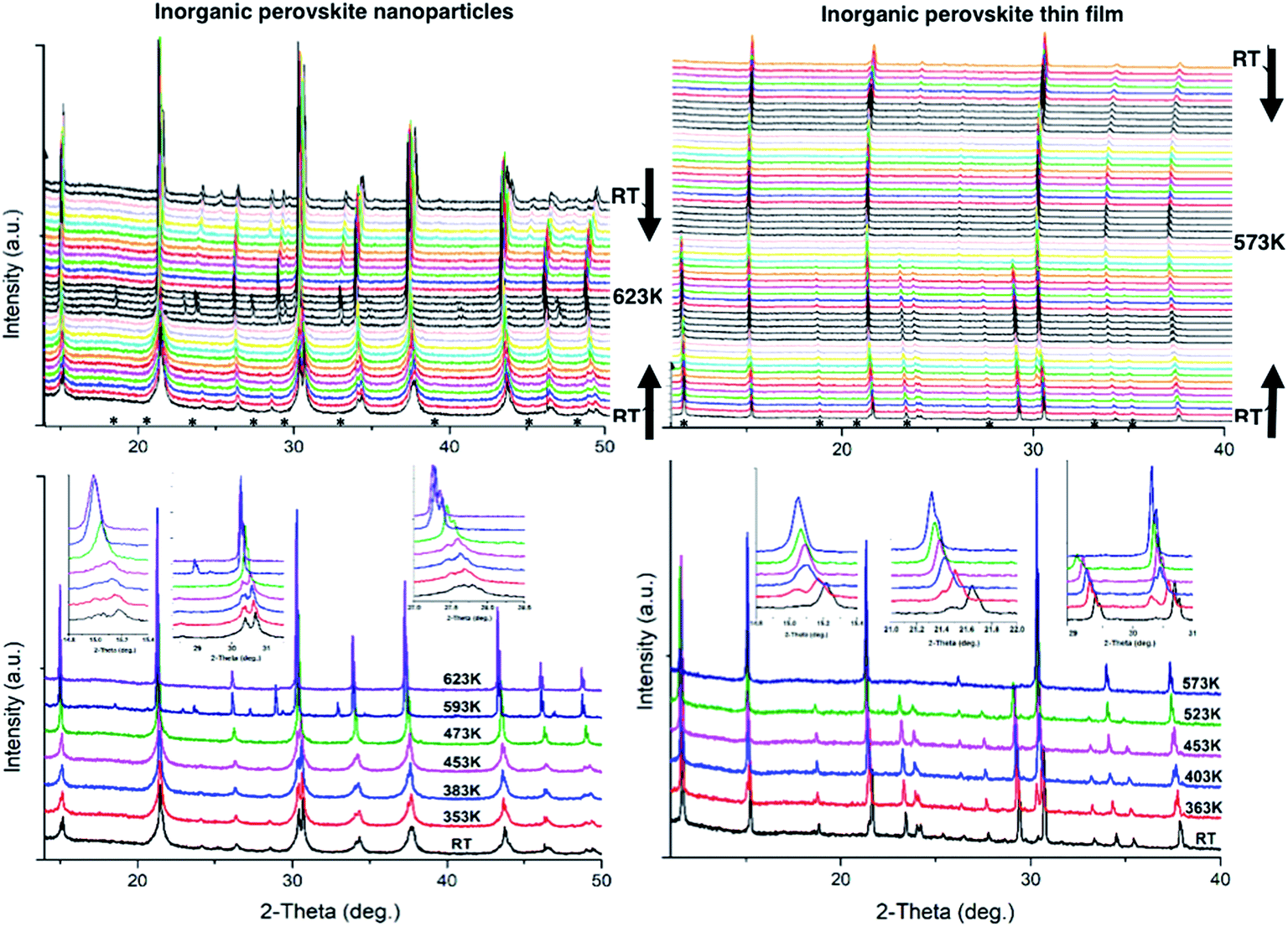 | ||
| Fig. 1 X-ray diffraction patterns recorded in situ at different temperatures for (left) CsPbBr3-based nanoparticles and (right) thin films. Scan step is every 15 K from 308 K to 623 K (top left) and every 10 K in the 303–573 K temperature range (top right) upon cooling and heating. Selected XRD patterns are shown with particular areas in insets. Asterisk symbolizes the CsPb2Br5 phase. | ||
Profile matching refinements using the Rietveld method and the FULLPROF program were performed on all the XRD data as a function of temperature in order to verify the phase symmetries and precisely determine the unit cell variations. Cell parameters, zero shift and peak shape factors (U, V and W from Caglioti's formula) were refined for each pattern. Fig. 2 shows the refined data at RT before and after in situ XRD thermal treatment, as well as at the highest temperature for both NPs and thin films. A very good match was found between the observed and calculated data (all reliability factors are 2.2 < χ2 < 4.7 and 0.12 < Rwp < 0.26, after Rietveld refinements), confirming the theoretical models, and refinements can be used for precisely determining the crystal unit cell at different temperatures. Note that peak shapes are sharper at RT after annealing owing to crystal size growth after the heating process.
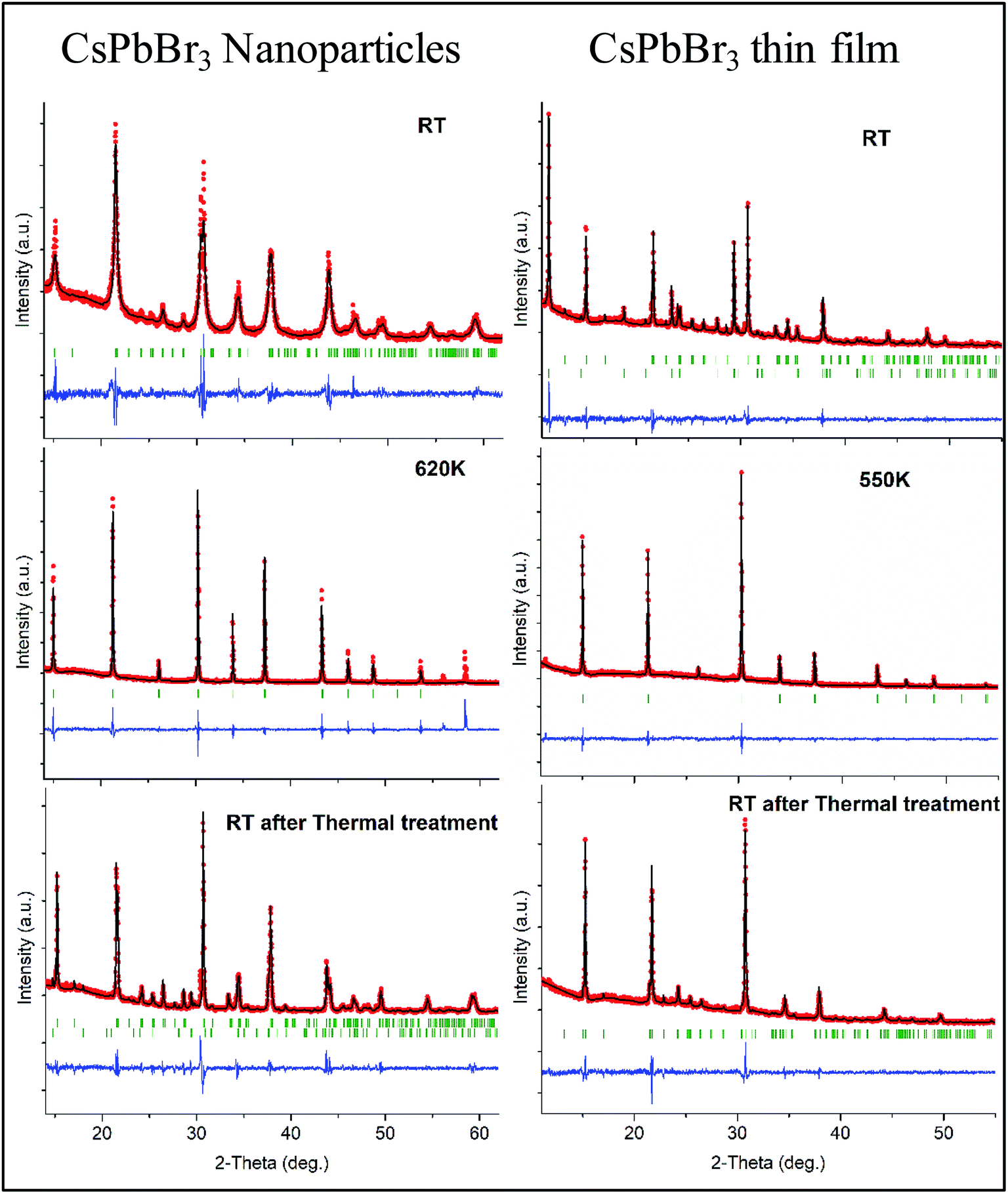 | ||
| Fig. 2 Profile matching of the XRD patterns for (left) CsPbBr3-based NPs and (right) thin films. At RT before in situ XRD heating measurements (top), highest temperature (middle) and back to RT (bottom). Symbols correspond to the observed (red dots), calculated (black line), difference (blue line below) XRD patterns and Bragg peaks (green vertical lines). | ||
Fig. 3b shows the unit cell parameters changes with temperature. In the case of the NPs, the orthorhombic structure is described with the Pnma space group (also mentioned in the literature as Pbnm with a different origin choice),6,12 and cell parameters are a = 8.240(2) Å, b = 11.755(2) Å and c = 8.210(2) Å. The peak shifts observed with the temperature increase correspond to a thermal cell expansion and for the cubic phase the cell parameter is equal to 5.9061(4) Å (Pm![[3 with combining macron]](https://www.rsc.org/images/entities/char_0033_0304.gif) m) at 623 K. When cooling down to RT, the orthorhombic CsPbBr3 phase exhibits a = 8.2638(5) Å, b = 11.6107(7) Å and c = 8.1959(6) Å unit cell parameters. The peak full width at half maximum (FWHM or Hw) is then on average half the value (for instance, Hw = 0.13 at 2-theta = 15.1°) of the one measured before heat treatment (Hw = 0.28), characterizing a wider crystallite size. A bigger change in the ‘c’ unit cell parameter is observed for the NPs compared to the thin film between heating and cooling, which indicates that there might be a preferred orientation or stronger distortion along the c-axis during the synthesis process. The distorted octahedral environments of Pb2+ and unit cell differences are attenuated owing to structural rearrangement after heating. The minority phase CsPb2Br5 left at RT after thermal treatment, presents a = b = 8.484(1) Å and c = 17.362(2) Å cell parameters with I4/mcm space group. The temperature and excess Pb2+ are two key factors for the formation of CsPbBr3/CsPb2Br5 mixtures. During the synthesis processes, the evolution between CsPb2Br5 and CsPbBr3 is reversible in a solution of superfluous Pb2+ and Br−. In our case, pure nanocrystals of cube-like shape were obtained at RT and upon heating in air these nanoparticles drive to the appearance of a small quantity of CsPb2Br5 dispersed with the main CsPbBr3 phase. Li et al.9 showed that tetragonal CsPb2Br5 nanosheets are obtained by an oriented attachment of orthorhombic CsPbBr3 nanocubes by varying the ligands, involving a lateral shape evolution from octagonal to square. The shape and phase evolution from CsPbBr3 to CsPb2Br5 demonstrated that the reaction could take place at 397 K (in the solvent with a negative Gibbs variation). CsPb2Br5 prefers growing horizontally at two crystal facets (100) and (110) and forms 2D layer structures with Pb and Br elements while Cs is between the two layers. As the nanocrystals grew, the evolution between CsPbBr3 and CsPb2Br5 persisted. However, CsPb2Br5 changes back to CsPbBr3 if sufficient Cs+ remains (in solution) at a relatively high temperature of 463 K. In the case of thin films, both CsPb2Br5 and CsPbBr3 phases coexists at RT. The orthorhombic CsPbBr3 phase shows cell values of a = 8.583(6) Å, b = 11.648(7) Å and c = 8.2081(4) Å, while for the majority phase CsPb2Br5, a = b = 8.4923(4) Å and c = 15.194(1) Å. At 573 K, a = 5.8972(3) Å for the cubic CsPbBr3. Once cooled down to RT, orthorhombic CsPbBr3 presents a = 8.2506(6) Å, b = 11.773(2) Å and c = 8.1878(5) Å cell parameters. Note that the intermediate phase of tetragonal symmetry (‘tet’ corresponds to ‘tetragonal’ in Fig. 3b), usually described in the literature6,13 from 360–400 K in the case of CsPbBr3, cannot be clearly distinguished here on the XRD patterns (Fig. 1). Indeed, the peaks observed at 2θ ∼ 24° and 29° in the XRD patterns corresponding to the orthorhombic phase remain up to 390 K while the peak splitting observed at 2θ ∼ 15° and 30.5° can still be attributed to the low temperature orthorhombic (Pnma) structure. In addition, profile matching refinements performed with either orthorhombic or tetragonal (P4/mbm) symmetry at 370 K show good pattern matching in both cases, with a reliability factor actually slightly improved for the former one (χ2 = 2.4 and 3.7, respectively), corresponding to a more distorted structure. Additional peaks corresponding to the CsPb2Br5 (and possibly CsPb4Br6) are observed in the XRD patterns of both nanoparticles and thin films from 500 to 595 K, which remain in small amounts upon cooling down to RT. For thin films, the main CsPb2Br5 phase starts to disappear upon heating above 500 K and is at a very low quantity above 570 K, while the cubic CsPbBr3 is the main phase at the highest temperatures (see Fig. 1). Our thin films were then re-heated to 623 K in order to check their behavior and stability. The CsPb2Br5 secondary phase disappears completely above 580 K and pure cubic CsPbBr3 is observed up to 623 K. This phase is then kept upon cooling down to RT with the usual symmetry distortion observed at T ∼ 390 K (Fig. 3a).
m) at 623 K. When cooling down to RT, the orthorhombic CsPbBr3 phase exhibits a = 8.2638(5) Å, b = 11.6107(7) Å and c = 8.1959(6) Å unit cell parameters. The peak full width at half maximum (FWHM or Hw) is then on average half the value (for instance, Hw = 0.13 at 2-theta = 15.1°) of the one measured before heat treatment (Hw = 0.28), characterizing a wider crystallite size. A bigger change in the ‘c’ unit cell parameter is observed for the NPs compared to the thin film between heating and cooling, which indicates that there might be a preferred orientation or stronger distortion along the c-axis during the synthesis process. The distorted octahedral environments of Pb2+ and unit cell differences are attenuated owing to structural rearrangement after heating. The minority phase CsPb2Br5 left at RT after thermal treatment, presents a = b = 8.484(1) Å and c = 17.362(2) Å cell parameters with I4/mcm space group. The temperature and excess Pb2+ are two key factors for the formation of CsPbBr3/CsPb2Br5 mixtures. During the synthesis processes, the evolution between CsPb2Br5 and CsPbBr3 is reversible in a solution of superfluous Pb2+ and Br−. In our case, pure nanocrystals of cube-like shape were obtained at RT and upon heating in air these nanoparticles drive to the appearance of a small quantity of CsPb2Br5 dispersed with the main CsPbBr3 phase. Li et al.9 showed that tetragonal CsPb2Br5 nanosheets are obtained by an oriented attachment of orthorhombic CsPbBr3 nanocubes by varying the ligands, involving a lateral shape evolution from octagonal to square. The shape and phase evolution from CsPbBr3 to CsPb2Br5 demonstrated that the reaction could take place at 397 K (in the solvent with a negative Gibbs variation). CsPb2Br5 prefers growing horizontally at two crystal facets (100) and (110) and forms 2D layer structures with Pb and Br elements while Cs is between the two layers. As the nanocrystals grew, the evolution between CsPbBr3 and CsPb2Br5 persisted. However, CsPb2Br5 changes back to CsPbBr3 if sufficient Cs+ remains (in solution) at a relatively high temperature of 463 K. In the case of thin films, both CsPb2Br5 and CsPbBr3 phases coexists at RT. The orthorhombic CsPbBr3 phase shows cell values of a = 8.583(6) Å, b = 11.648(7) Å and c = 8.2081(4) Å, while for the majority phase CsPb2Br5, a = b = 8.4923(4) Å and c = 15.194(1) Å. At 573 K, a = 5.8972(3) Å for the cubic CsPbBr3. Once cooled down to RT, orthorhombic CsPbBr3 presents a = 8.2506(6) Å, b = 11.773(2) Å and c = 8.1878(5) Å cell parameters. Note that the intermediate phase of tetragonal symmetry (‘tet’ corresponds to ‘tetragonal’ in Fig. 3b), usually described in the literature6,13 from 360–400 K in the case of CsPbBr3, cannot be clearly distinguished here on the XRD patterns (Fig. 1). Indeed, the peaks observed at 2θ ∼ 24° and 29° in the XRD patterns corresponding to the orthorhombic phase remain up to 390 K while the peak splitting observed at 2θ ∼ 15° and 30.5° can still be attributed to the low temperature orthorhombic (Pnma) structure. In addition, profile matching refinements performed with either orthorhombic or tetragonal (P4/mbm) symmetry at 370 K show good pattern matching in both cases, with a reliability factor actually slightly improved for the former one (χ2 = 2.4 and 3.7, respectively), corresponding to a more distorted structure. Additional peaks corresponding to the CsPb2Br5 (and possibly CsPb4Br6) are observed in the XRD patterns of both nanoparticles and thin films from 500 to 595 K, which remain in small amounts upon cooling down to RT. For thin films, the main CsPb2Br5 phase starts to disappear upon heating above 500 K and is at a very low quantity above 570 K, while the cubic CsPbBr3 is the main phase at the highest temperatures (see Fig. 1). Our thin films were then re-heated to 623 K in order to check their behavior and stability. The CsPb2Br5 secondary phase disappears completely above 580 K and pure cubic CsPbBr3 is observed up to 623 K. This phase is then kept upon cooling down to RT with the usual symmetry distortion observed at T ∼ 390 K (Fig. 3a).
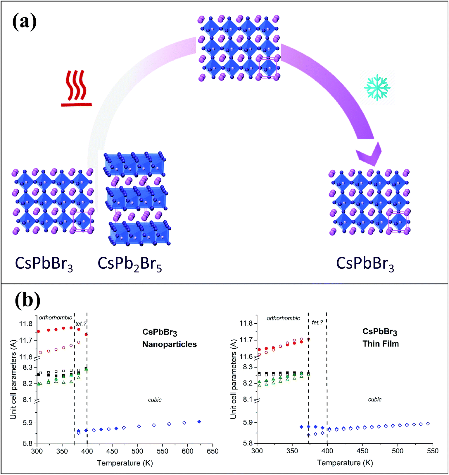 | ||
| Fig. 3 (a) Schematic illustration of the process described in this work. On heating the CsPbBr3 thin films to 623 K, the CsPb2Br5 disappears and pure CsPbBr3 remains when cooling down to room temperature. (b) Cell parameters as a function of temperature for (left) NPs and (right) thin films. Triangles, squares and circles correspond to the a, b and c unit cell parameters, respectively. Closed and open symbols correspond to the heating and cooling sequence, respectively. The uncertainty of the cell value is contained within each symbol. ‘tet’ corresponds to tetragonal. | ||
Annealing films made of CsPbBr3 nanoparticles can lead to morphological transformations (sintering) and chemical transformations (transformation and vanishing of tetragonal CsPb2Br5 phase) that could be linked to the desorption of different organic species from the film at different temperatures.14 Post-synthesis transformation of insulating Cs4PbBr6 into bright perovskite CsPbBr3 can also be performed through thermal annealing by physical extraction of CsBr.15 The extracted Cs+ and Br− ions would be complexed by residual organics or form very small clusters hardly detectable by XRD. CsPb2Br5 could recombine with CsBr by the following reaction: CsPb2Br5 + CsBr = 2CsPbBr3. Similarly, during the annealing process of our thin films initially containing a mixture of CsPb2Br5 and CsPbBr3, CsPb2Br5 can transform into CsPbBr3 releasing ions of Pb2+ and 2Br− (PbBr2), which can spontaneously react with Cs4PbBr6 in order to form pure CsPbBr3 (Cs4PbBr6 + 3PbBr2 = 4CsPbBr3). Therefore, small quantities or clusters of CsBr and PbBr2 extracted during the annealing process will contribute to the phase transformations and, if in appropriate proportions, to the formation of pure CsPbBr3 that can remain down to RT.
Top view scanning electron microscopy (SEM) images of the CsPbBr3 thin film can be observed in Fig. 4. The CsPbBr3 thin films were annealed to 338 K, 368 K, 398 K, 428 K, 458 K, 503 K, 563 K and 623 K in order to get some observations on the film morphology while heating. Upon increasing the temperature, the perovskite grains melt together, losing their shape, while the XRD measurements show that their crystallinity is maintained.
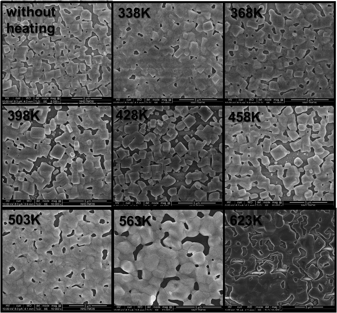 | ||
| Fig. 4 SEM top view images of CsPbBr3 thin films at different annealing temperatures. Scale bar is 5 μm. | ||
The case of the CsPbBr3 NPs is different. Transmission electron microscopy (TEM) images at three annealing temperatures are shown in Fig. 5.
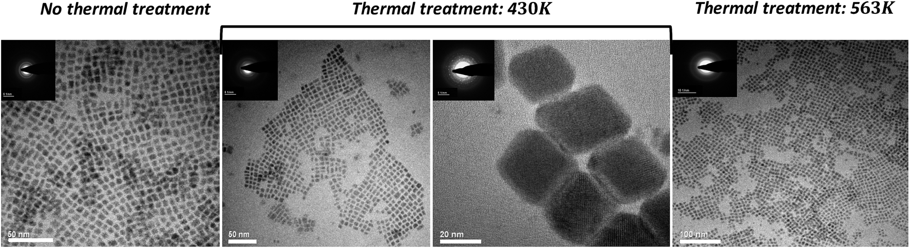 | ||
| Fig. 5 TEM micrographs of CsPbBr3 and CsPb2Br5 NPs after different annealing temperatures. Insets correspond to the electron diffraction patterns taken from these NPs. | ||
The NPs were synthesized using the metathesis reaction, which involves the injection of Cs-oleate precursor into a hot mixture of PbBr2, octadecene, and ligand (oleic-acid and oleylamine). After the Cs-oleate injection, the mixture was cooled down with an ice bath. At this point, before the purification process, a thermal treatment was performed. The NPs crude mixture were heated slowly to 430 K and 563 K, for comparison.
In the case of the NPs without thermal treatment (i.e. “no thermal treatment”) a typical size of 6 ± 1 nm and cubic-like shape are observed. The d-spacing values, calculated from the electron diffraction patterns, are d = 4.2 Å which is related to the most intense peaks and close to each other in XRD, i.e. (112) and (020); d = 2.9 Å related to the second most intense peak (220) in the XRD and d = 2.0 Å related to (224) and (040) crystallographic planes. Based on these d-spacing, the NPs are in the orthorhombic phase at RT.
TEM images of the NPs after annealing to 430 K can be seen in the middle of Fig. 5. Two different sizes of NPs were observed. A set of small NPs with size distribution of 6 ± 1 nm, and large NPs in the size of 28 ± 4 nm. The d-spacing determined after measuring the distances from the center of electron diffraction pattern to the diffracted lines are d = 3.0 Å and d = 2.1 Å for the small NPs close to the (220), (224) and (040) planes of the orthorhombic symmetry of CsPbBr3 while for the large NPs the d-spacing are d = 2.6 Å, d = 2.3 Å and d = 1.60 Å, which can be attributed to the (310), (313) and (504) planes also observed by XRD for the tetragonal phase of CsPb2Br5. This further confirms the presence of the CsPb2Br5 phase in the NPs.
In the case of the annealing treatment up to 563 K, a change to the color of the crude solution was observed during the annealing process owing to the precipitation of large NPs (larger than in the case of 430 K). It can be assumed that the large NPs contain the CsPb2Br5 phase as predicted in the case of 430 K annealing and while heating further to 563 K these NPs keep on growing, making them too large to be analyzed by TEM. As mentioned earlier, the XRD measurements above 500 K recognized the CsPb2Br5 phase in the NPs samples, which further supports our assumption. Fig. 5 shows the small NPs that were observed in parallel to the very large NPs after the annealing treatment to 563 K. Analyzing their electron diffraction patterns once back at RT provides the corresponding d-spacing: d = 2.5 Å and d = 2.1 Å; these values match with the orthorhombic phase of CsPbBr3, the regular stable phase at room temperature.
Conclusions
This work describes a detailed structural study on CsPbBr3 thin films and NPs. In situ XRD as a function of the temperature was acquired systematically each 10–15 K, where the lattice parameters and the phases of cesium lead bromide perovskite were tracked upon heating above RT. Both thin films and NPs exhibit the orthorhombic phase at RT while their cubic phase was revealed upon heating to 623 K. In both cases the parasitic CsPb2Br5 phase is observed at 500 K, where from 500 K to 595 K, this phase remains in small amounts and kept like this upon cooling down to RT. Interestingly in the case of thin films, further heating to 623 K results in complete elimination of the CsPb2Br5 phase, which remains like this when cooled down back to RT. In addition, a bigger change in the ‘c’ unit cell parameter is observed for NPs compares to thin films between heating and cooling, which indicates that there might be a preferred orientation or stronger distortion along the c-axis during the synthesis process. The distorted octahedral environments of Pb2+ and the unit cell differences are attenuated owing to structural rearrangement after heating. SEM and TEM characterization support the different morphologies and phases observed by the XRD. This study shows the importance of understanding the structural changes in all-inorganic perovskites and provides a route to achieve pure CsPbBr3 phase.Experimental
XRD measurements
In situ X-ray diffraction (XRD) measurements were performed in air with a Bruker AXS D8-ADVANCE instrument in the Bragg–Brentano configuration (with copper radiation CuKalpha1 = 1.5405 Å and CuKalpha2 = 1.5445 Å) equipped with an Anton-Paar HTK1200N heating system. Samples were heated up to a maximum temperature of 623 K with heating and cooling rates of 10 °C min−1. XRD patterns were recorded every 10–15 K from 10 to 60° in 2-theta with a step scan of 0.014° and 0.3 s per step. An approximately 1.5 cm2 square shape glass sample with the nanoparticles in a solvent spread over with a spatula or as-prepared thin films was put on the alumina sample holder close to the S-type platinum (Rh10Pt) thermocouple.CsPbBr3 NPs synthesis and characterization
CsPbBr3 NPs were synthesized according to a previously published procedure,3 which was slightly adjusted. Lead bromide (PbBr2, 99.9%), cesium carbonate (Cs2CO3, 99.9%), octadecene (ODE, Tech. 90%), oleic acid (OA, Tech. 90%), and oleylamine (OLA, Tech. 70%) were purchased from Sigma-Aldrich. Briefly, 0.207 g of PbBr2 was dissolved in 15 mL of ODE, 1.5 mL of OA, and 1.5 mL of OLA in a three-necked-flask, and then degassed at 393 K. 0.4 g of Cs2CO3 was dissolved in 15 mL of ODE and 1.25 mL of OA in a three-necked-flask, and degassed at 393 K. Then, under argon atmosphere, a hot syringe was used to swiftly inject 1.2 mL of the Cs precursor into the PbBr2 precursor solution (which was at 393 K). The reaction was quenched with an ice bath for 10 seconds after the injection of the Cs precursor, yielding a shiny green-yellow colloid. The colloid was then divided into three vials, two of which were thermally treated: one vial was heated to 428 K, while the other was heated to 563 K. The third vial did not undergo any thermal treatment. Finally, the NPs were precipitated by centrifugation (6000 rpm for 10 minutes), and the supernatant was discarded. The NPs were re-dispersed in hexane, and bulky byproducts were precipitated by centrifugation (3000 rpm for 5 minutes).CsPbBr3 films deposition
CsPbBr3 films were prepared on clean microscope glass substrates by two-step deposition technique (as described in ref. 16). Briefly, a 1 M solution of PbBr2 (≥98% Sigma-Aldrich) in dimethylformamide and a 20 mg mL−1 CsBr solution (99.999% Sigma-Aldrich) in methanol were dissolved overnight on a hot plate at 70 °C and 50 °C, respectively. PbBr2 solution was spin-coated for 30 s at 1200 rpm and dried on a hot plate at 70 °C for 10 min. After drying, the substrates were dipped for 5 min in a hot solution of CsBr (50 °C) and annealed for 10 min at 250 °C.For the thermal treatment, a hot plate was heated stepwise starting at 30 °C reaching up to 563 K. The CsPbBr3 films were placed on the hot plate. The gradual heating process included the following temperatures: 303 K, 338 K, 368 K, 398 K, 428 K, 458 K, 503 K, 563 K and 623 K, where the temperature was kept constant at each value for 20 minutes.
![[thin space (1/6-em)]](https://www.rsc.org/images/entities/char_2009.gif) 000.
000.
Conflicts of interest
There are no conflicts to declare.Acknowledgements
The French FERMAT Federation FR3089 is acknowledged for financial support for the D8 XRD instrument and M. Benjamin Duployer, from the CIRIMAT laboratory, for experimental assistance. We would like to thank the Israel Ministry of Energy for supporting this work.References
- W. S. Yang, B.-W. Park, E. H. Jung, N. J. Jeon, Y. C. Kim, D. U. Lee, S. S. Shin, J. Seo, E. K. Kim, J. H. Noh and S. I. Seok, Iodide management in formamidinium-lead-halide-based perovskite layers for efficient solar cells, Science, 2017, 356(6345), 1376–1379 CrossRef CAS PubMed.
- C. K. Møller, Crystal Structure and Photoconductivity of Cæsium Plumbohalides, Nature, 1958, 182, 1436 CrossRef.
- L. Protesescu, S. Yakunin, M. I. Bodnarchuk, F. Krieg, R. Caputo, C. H. Hendon, R. X. Yang, A. Walsh and M. V. Kovalenko, Nanocrystals of Cesium Lead Halide Perovskites (CsPbX3, X = Cl, Br, and I): Novel Optoelectronic Materials Showing Bright Emission with Wide Color Gamut, Nano Lett., 2015, 15, 3692 CrossRef CAS PubMed.
- M. Koolyk, D. Amgar, S. Aharon and L. Etgar, Kinetics of cesium lead halide perovskite nanoparticle growth; focusing and de-focusing of size distribution, Nanoscale, 2016, 8, 6403–6409 RSC.
- C. C. Stoumpos, C. D. Malliakas, J. A. Peters, Z. Liu, M. Sebastian, J. Im, T. C. Chasapis, A. C. Wibowo, D. Y. Chung, A. J. Freeman, B. W. Wessels and M. G. Kanatzidis, Crystal Growth of the Perovskite Semiconductor CsPbBr3: A New Material for High-Energy Radiation Detection, Cryst. Growth Des., 2013, 13, 2722 CrossRef CAS.
- C. C. Stoumpos, C. D. Malliakas and M. G. Kanatzidis, Semiconducting Tin and Lead Iodide Perovskites with Organic Cations: Phase Transitions, High Mobilities, and Near-Infrared Photoluminescent Properties, Inorg. Chem., 2013, 52, 9019 CrossRef CAS PubMed.
- P. Cottingham and R. L. Brutchey, On the crystal structure of colloidally prepared CsPbBr3 quantum dots, Chem. Commun., 2016, 52, 5246 RSC.
- S. K. Balakrishnan and P. V. Kamat, Ligand Assisted Transformation of Cubic CsPbBr3 Nanocrystals into Two-Dimensional CsPb2Br5 Nanosheets, Chem. Mater., 2018, 30, 74–78 CrossRef CAS.
- G. Li, H. Wang, Z. Zhu, Y. Chang, T. Zhang, Z. Song and Y. Jiang, Shape and phase evolution from CsPbBr3 perovskite nanocubes to tetragonal CsPb2Br5 nanosheets with an indirect bandgap, Chem. Commun., 2016, 52, 11296 RSC.
- X. Zhang, B. Xu, J. Zhang, Y. Gao, Y. Zheng, K. Wang and X. W. Sun, All-Inorganic Perovskite Nanocrystals for High-Efficiency Light Emitting Diodes: Dual-Phase CsPbBr3–CsPb2Br5 Composites, Adv. Funct. Mater., 2016, 26, 4595–4600 CrossRef CAS.
- I. Dursun, M. De Bastiani, B. Turedi, B. Alamer, A. Shkurenko, J. Yin, A. M. El-Zohry, I. Gereige, A. Ahmed, O. F. Mohammed, E. Mohamed and O. M. Bakr, CsPb2Br5 Single Crystals: Synthesis and Characterization, ChemSusChem, 2017, 10, 3746–3749 CrossRef CAS PubMed.
- M. Imran, F. Di Stasio, Z. Dang, C. Canale, A. H. Khan, J. Shamsi, R. Brescia, M. Prato and L. Manna, Colloidal Synthesis of Strongly Fluorescent CsPbBr3 Nanowires with Width Tunable down to the Quantum Confinement Regime, Chem. Mater., 2016, 28(18), 6450–6454 CrossRef CAS PubMed.
- M. Zhang, Z. Zheng, Q. Fu, Z. Chen, J. He, S. Zhang, L. Yan, Y. Hua and W. Luo, Growth and characterization of all-inorganic lead halide perovskite semiconductor CsPbBr3 single crystals, CrystEngComm, 2017, 19, 6797–6803 RSC.
- F. Palazon, S. Dogan, S. Marras, F. Locardi, I. Nelli, P. Rastogi, M. Ferretti, M. Prato, K. Roman and L. Manna, From CsPbBr3 Nano-Inks to Sintered CsPbBr3–CsPb2Br5 Films via Thermal Annealing: Implications on Optoelectronic Properties, J. Phys. Chem. C, 2017, 121(21), 11956–11961 CrossRef CAS.
- F. Palazon, C. Urso, L. De Trizio, Q. Akkerman, S. Marras, F. Locardi, I. Nelli, M. Ferretti, M. Prato and L. Manna, Postsynthesis Transformation of Insulating Cs4PbBr6 Nanocrystals into Bright Perovskite CsPbBr3 through Physical and Chemical Extraction of CsBr, ACS Energy Lett., 2017, 2, 2445–2448 CrossRef CAS PubMed.
- M. Kulbak, D. Cahen and G. Hodes, How Important Is the Organic Part of Lead Halide Perovskite Photovoltaic Cells? Efficient CsPbBr3 Cells, J. Phys. Chem. Lett., 2015, 6, 2452–2456 CrossRef CAS PubMed.
| This journal is © The Royal Society of Chemistry 2019 |