
 Open Access Article
 This Open Access Article is licensed under a Creative Commons Attribution-Non Commercial 3.0 Unported Licence
Rational design of C2N-based type-II heterojunctions for overall photocatalytic water splitting†
Xu
Zhang
,
An
Chen
,
Zihe
Zhang
,
Menggai
Jiao
and
Zhen
Zhou
 *
*
School of Materials Science and Engineering, National Institute for Advanced Materials, Institute of New Energy Material Chemistry, Computational Centre for Molecular Science, Nankai University, Tianjin 300350, P. R. China. E-mail: zhouzhen@nankai.edu.cn; Fax: +86 22 23498941; Tel: +86 22 23503623
First published on 11th September 2018
Abstract
Photocatalytic water splitting is a promising method for the production of clean energy and searching for efficient photocatalysts has received extensive attention. Fabricating type-II heterojunctions is an effective approach to improve the photocatalytic efficiency. Based on the band edge positions and lattice parameters, we found that several kinds of monochalcogenide monolayers can be used to fabricate type-II heterojunctions with C2N monolayers. C2N/GaTe and C2N/InTe van der Waals (vdW) heterojunctions were investigated as potential photocatalysts for water splitting by means of first-principles computations. Both are type-II heterojunctions, and could promote the efficient spatial separation of electron–hole pairs. Their band edges straddle water redox potentials, satisfying the requirements for photocatalytic water splitting. Besides, the high carrier mobility of C2N/GaTe and C2N/InTe heterojunctions implies that the transfer of carriers to reactive sites is easy, and the recombination probability of photo-generated carriers is reduced. The Gibbs free energy calculations indicate that C2N/GaTe and C2N/InTe heterojunctions, especially C2N/InTe, exhibit high catalytic performance towards hydrogen and oxygen evolution reactions. Particularly, C2N/InTe exhibits a direct band gap with strong absorption in both visible and near ultraviolet regions, indicating that it is a very promising candidate for photocatalytic water splitting. This work would provide a new idea for the development of type-II heterojunctions for photocatalytic water splitting.
Introduction
Photocatalytic water splitting is a promising technology to produce hydrogen with sunlight, providing a sustainable solution to address environmental and energy related issues.1,2 The first significant breakthrough in photocatalytic overall water splitting without electric power was achieved by Fujishima and Honda.3 Since then, many photocatalysts have been developed.4–10 However, industrial hydrogen is primarily produced from fossil fuels since the current photocatalytic systems are not efficient and economical enough for industrial hydrogen production.4 A low quantum yield, inability to utilize visible light and poor catalytic activity are critical obstacles for the commercial application of photocatalytic water splitting.11,12 Therefore, the discovery of novel photohydrolytic catalysts with high efficiency plays a critical role in the development of photocatalytic water splitting.Nanoscale materials with adjustable dimensions and shapes are one of the most promising photohydrolytic catalysts. Among various kinds of nanoscale materials, two-dimensional (2D) materials possess two main inherent advantages which can be used to improve the photocatalytic efficiency for water splitting.11,13–15 First, 2D materials have a high surface to volume ratio, exhibiting a large specific surface area available for photocatalytic reactions and promoting the adsorption of reactants. Besides, the distance that photo-generated electrons and holes have to migrate in 2D materials is short, reducing the possibility of electron–hole recombination, thereby potentially enhancing photocatalytic activity. With the rapid development of high-performance computations, various 2D materials were designed and predicted to be promising photocatalysts for overall water splitting.11,12,15,16 The computations have promoted the development of photocatalysts and some 2D materials have been proved to be good photocatalysts for water splitting in experiments, such as g-C3N4 (ref. 17) and MPS3 (M = Fe or Mn).18,19
Besides, fabricating van der Waals (vdW) heterojunctions is an effective method to further improve the photocatalytic performance.20,21 Especially, in type-II heterojunctions, both the conduction band minimum (CBM) and valence band maximum (VBM) of one layer are lower than that of the other layer. Therefore, the lowest energy states of electrons and holes are on different layers, ensuring the effective separation of photo-generated electrons and holes. In our previous reports, we proposed a high-throughput computational material design framework to search for 2D photocatalysts and rationally design type-II heterojunctions for water splitting based on the Materials Project Database.15 Various kinds of type-II heterojunctions were successfully designed. However, due to the rapid development of 2D materials, several novel kinds of materials, which have not been included in materials databases, have been successfully prepared in experiments. Therefore, predicting type-II heterojunctions containing novel kinds of 2D materials is necessary to evaluate their photocatalytic activity.
Recently, a novel kind of 2D material, named C2N, has been successfully prepared by simple wet chemical reactions.22 By means of first-principles computations, C2N monolayers were predicted to be a promising photocatalyst for water splitting.23 In experiments, vdW heterojunctions composed of C2N and aza-conjugated microporous polymers were prepared, which exhibit good photocatalytic performance for overall water splitting.24 Enlightened by the computational and experimental results, we screened the 2D monolayer materials in our previous work15 to explore the materials which could be used to fabricate type-II heterojunctions with C2N monolayers to further improve their photocatalytic performance. The screening criteria are consistent with our previous report.15 First, the CBM and VBM of the layer should be lower or higher than that of C2N, respectively. Then the lattice parameters of the layer should be close to those of C2N (lattice mismatch <10%), which could reduce the strain, improving the stability. This could also be achieved by constructing supercells. Considering the computational cost, small supercells, such as 2 × 2 × 1 supercells, were considered. Our results indicate that transition metal monochalcogenides and dichalcogenides could be used to fabricate type-II vdW heterojunctions with C2N. Recently, C2N/WS2 vdW type-II heterojunctions were proposed as promising photocatalysts for water splitting.25
Therefore, in this work, we focused on monochalcogenide/C2N heterojunctions. Based on the calculated band structures,26 besides GaTe which was proposed in our previous report,15 some other monochalcogenides, including GaSe and InTe, were also investigated. By means of first-principles computations, we designed GaSe/C2N, GaTe/C2N and InTe/C2N vdW heterojunctions and investigated their stability, electronic, optical properties, carrier mobility and catalytic performance towards the hydrogen evolution reaction (HER) and oxygen evolution reaction (OER). The results indicate that GaTe/C2N and InTe/C2N are type-II heterojunctions, implying the efficient separation of holes and electrons, thereby preventing their recombination. The exciton binding energies of GaTe/C2N and InTe/C2N type-II heterojunctions are lower than that of C2N, indicating better separation of the bound holes and electrons to free charge carriers. Both GaTe/C2N and InTe/C2N exhibit high carrier mobility, indicating high photocatalytic activity. Besides, InTe/C2N exhibits an excellent catalytic performance towards the HER and OER, further proving InTe/C2N type-II heterojunctions to be a promising candidate for overall photocatalytic water splitting.
Computational methods
First-principles computations on the basis of density functional theory (DFT) were performed by using a plane-wave basis set as implemented in the Vienna ab initio simulation package (VASP).27 Ion-electron interactions were described with the projector augmented wave (PAW) method28 and an energy cutoff of 550 eV was adopted for the plane-wave basis set. The generalized gradient approximation (GGA) involving the Perdew, Burke, and Ernzerhof (PBE) functional was selected to describe the exchange correlation energy.29 The effect of the vdW interactions was dealt with the DFT-D3 method with Becke–Jonson damping.30,31 A Monkhorst–Pack k-point mesh32 of 5 × 5 × 1 was employed for C2N and heterojunctions and 10 × 10 × 1 for monochalcogenide (MX, M = Ga, In, X = Se, Te) monolayers. In order to prevent the artificial interactions between periodic images, a vacuum space with at least 20 Å was inserted between the periodic images along the z-direction. Since the GGA functional systematically underestimates the band gaps,33 we used the Heyd–Scuseria–Ernzerhof (HSE06) functional34 to accurately compute the band structures and band edge positions.The binding energy of vdW heterojunctions was calculated based on:
| Ebinding = Eheterojunction − EC2N − EMX |
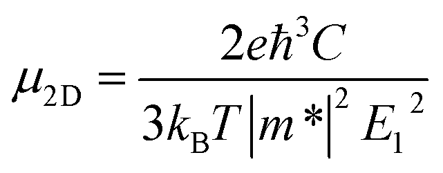
For inorganic semiconductors, the phonon scattering dominates the intrinsic mobility which could be described by deformation potential (DP) theory.35 DP theory has been successfully used in predicting the carrier mobility of 2D semiconductors, including graphene,36 phosphorene,37 MoS2,38 MXenes39 and so on.16,40 Therefore, the carrier mobility (μ2D) of isolated C2N, GaTe, and InTe monolayers and heterojunctions could be predicted by using the phonon limited scattered mode on the basis of effective mass approximation with DP theory according to:
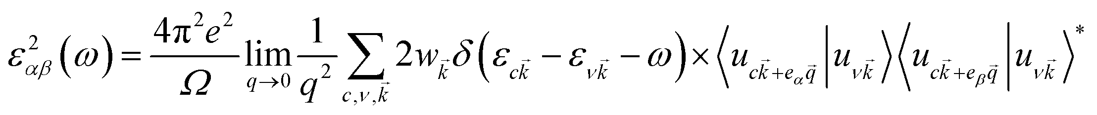
To investigate the optical absorption, the imaginary part of the dielectric function ε2 was calculated based on the following equation:41
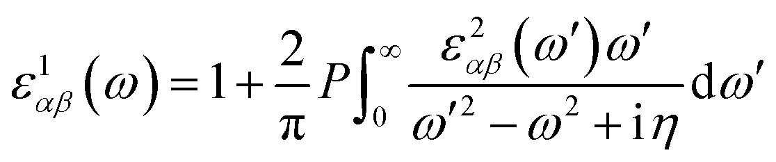
![[k with combining right harpoon above (vector)]](https://www.rsc.org/images/entities/i_char_006b_20d1.gif) represents the cell periodic part of the orbital at the k-point . The real part is obtained by using the Kramers–Kronig relationship:42
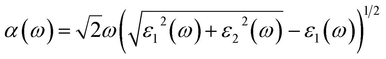
represents the cell periodic part of the orbital at the k-point . The real part is obtained by using the Kramers–Kronig relationship:42where P indicates the principal value. The absorption coefficient α(ω) was computed by using43
where ε1 is the real part of the dielectric function, obtained from ε2 by using the Kramer–Kronig relationship.
The HER catalytic performance of the heterojunctions was evaluated by calculating the Gibbs free energy change of the adsorption of atomic hydrogen (ΔGH):
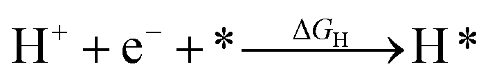
| ΔGH = ΔEH + ΔEZPE − TΔSH |
where R is the universal gas constant, h is Planck's constant, νi is the normal mode frequency, NA is Avogadro's number and N represents the number of the adsorbed atoms. The ΔGH of a good catalyst for the HER should be close to zero.

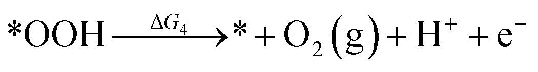
Under acidic conditions, the mechanism for the OER process is:
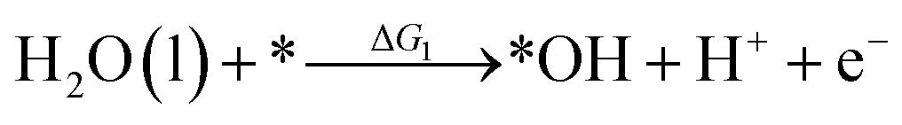
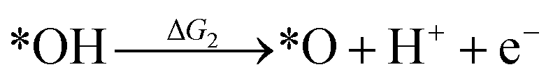
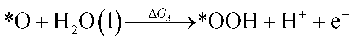
where (l) represents the liquid phase and (g) refers to the gas phase. To estimate the OER activity, the free energy change (ΔG) of the OER elementary steps should be calculated by:
| ΔG = ΔE + ΔEZPE − TΔS + ΔGU + ΔGpH |
![[thin space (1/6-em)]](https://www.rsc.org/images/entities/char_2009.gif) ln10 × pH. Because of the inaccuracy of DFT in estimating the binding energy of O2, the free energy of O2 was calculated according to the free energy change of O2 + 2H2 → 2H2O, which is −4.92 eV.
ln10 × pH. Because of the inaccuracy of DFT in estimating the binding energy of O2, the free energy of O2 was calculated according to the free energy change of O2 + 2H2 → 2H2O, which is −4.92 eV.
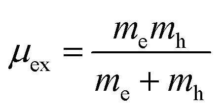
In order to evaluate the efficiency of the separation of photogenerated charge carriers, the exciton binding energies (Eb) were calculated based on the Mott–Wannier hydrogenic model. In a previous report, the exciton binding energies of C2N containing vdW heterojunctions were calculated based on:25
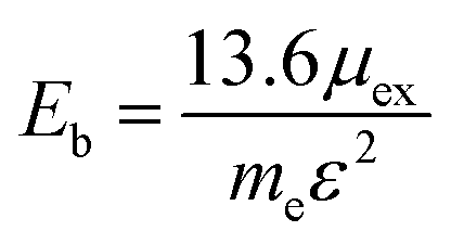
where μex is the effective exciton mass and ε is the macroscopic static dielectric constant which is the sum of the ionic εion and electronic εel contributions.
Results and discussion
Geometric structure and electronic properties of isolated monolayers
First the geometric structures of isolated monolayers were optimized and are shown in Fig. S1.† The lattice parameters are listed in Table S1,† which are consistent with reported values.26,46Then the electronic properties of these monolayers were investigated at the HSE06 level as shown in Fig. S2.† The C2N monolayer exhibits a direct band gap of 2.49 eV at the Γ point of the Brillouin zone, which agrees well with those in previous reports.23,46 The MX monolayers (GaSe, GaTe and InTe) exhibit indirect band gaps of 2.97, 2.21 and 2.21 eV, respectively. For GaSe and InTe monolayers, the CBM is at the Γ point while the VBM is located between the Γ and K points. For the GaTe monolayer, the CBM is located at the M point. These computational results are consistent with those in the previous report,26 indicating the reliability of our results.
Geometric structure and stability of heterojunctions
In order to match the lattice and reduce the strain, the C2N/MX heterojunctions were constructed based on the unit cell of C2N and 2 × 2 × 1 supercells of MX monolayers. Three high symmetry stacking patterns (Fig. S3†) were considered in this work. For pattern a, all the MX atoms are on the top of the hollow sites of the C2N monolayers. For patterns b and c, several MX atoms are located on the top of C2N atoms. The relative binding energies are shown in Table S2.† For all the heterojunctions, pattern a is the most stable structure and was used in the following computations.The geometric structures, lattice parameters and binding energies of the most stable structure for the three heterojunctions are summarized in Fig. 1 and Table S3.† The distance between the C2N and MX monolayers in these heterojunctions is about 3.40 Å (Table S3†), implying that the vdW effect plays the primary role in the interlayer interaction. Due to the large lattice mismatch for C2N/GaSe (Table S3†), the binding energy is positive, indicating that it is unstable. For C2N/GaTe and C2N/InTe, their lattice mismatch is lower than 3%, ensuring the experimental feasibility. Besides, the binding energies of C2N/GaTe and C2N/InTe are −10.8 and −9.6 meV Å−2, respectively, which are comparable to those of some typical vdW crystals, including MoS2 (−26.0 meV Å−2)47 and graphene (−12.0 meV Å−2),48 and some vdW heterojunctions, such as GaSe/graphene (−18.4 meV Å−2)49 and C3N4/MoS2 (−17.8 meV Å−2).50 These results further indicate that C2N/GaTe and C2N/InTe are stable. C2N/GaTe and C2N/InTe heterojunctions were investigated in the following computations.
 | ||
| Fig. 1 Top and side views of (a) C2N/GaSe, (b) C2N/GaTe and (c) C2N/InTe heterojunctions. | ||
Electronic and optical properties of heterojunctions
The electronic properties are extremely important for photocatalysts. The band structures of C2N/GaTe and C2N/InTe heterojunctions were calculated with the HSE06 functional as shown in Fig. 2.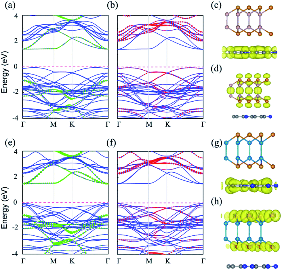 | ||
| Fig. 2 Band structures of the C2N/GaTe heterojunction projected to (a) C2N and (b) GaTe, respectively computed with the HSE06 functional. Band structures of the C2N/InTe heterojunction projected to (e) C2N and (f) InTe, respectively. The sizes of green and red dots represent the weight of C2N and GaTe (InTe). Spatial structures of wave functions for the C2N/GaTe heterojunction at the (c) CBM and (d) VBM with an isosurface of 0.002 e Å−3. Spatial structures of wave functions for the C2N/InTe heterojunction at the (g) CBM and (h) VBM with an isosurface of 0.002 e Å−3. | ||
The band gaps of C2N/GaTe and C2N/InTe heterojunctions are 1.43 and 1.52 eV, respectively, which are lower than those of isolated monolayers. The CBM of C2N/GaTe and C2N/InTe heterojunctions both are located at the Γ point. The VBM of C2N/GaTe is located between the Γ and K points while the VBM of C2N/InTe is at the Γ point. Therefore, C2N/InTe transfers to a direct band gap semiconductor while C2N/GaTe still possesses an indirect band gap. As shown in Fig. 2, the CBM of the heterojunctions is mainly contributed by C2N while the VBM mostly comes from the MX. Therefore, both C2N/GaTe and C2N/InTe possess a typical type-II band alignment, which promotes the efficient spatial separation of electron–hole pairs, overcoming the electron–hole recombination issue. The conduction band offset (CBO) and valence band offset (VBO) were calculated to be 0.65 and 1.00 eV for C2N/GaTe and 0.79 and 0.92 eV for C2N/InTe. The photogenerated electrons in the CBM of GaTe or InTe could transfer to the CBM of C2N by the chemical potential difference of CBO while the photogenerated holes in the VBM of C2N can migrate to the VBM of GaTe or InTe via the chemical potential difference of VBO. The results further ensure the effective spatial separation of electron–hole pairs.
Besides, the partial density of states (PDOS) was also calculated to gain deep insight into the composition of the VBM and CBM of the heterojunctions as shown in Fig. S4.† The CBM mainly originates from the p states of C and N atoms while the VBM is contributed by the p states of Te and Ga (or In) atoms.
A fundamental requirement for photocatalysts for overall water splitting is that the band edges should straddle the water redox potentials. That is to say, the VBM must be lower than the oxidation potential of O2/H2O and the CBM should be higher than the reduction potential of H+/H2. Besides, the water redox potential is influenced by the pH value.12,15 Here, the reduction potential of H+/H2 is calculated by using:  and the oxidation potential of O2/H2O is
  . The schematic diagram for the band edge positions relative to the vacuum level of the isolated monolayers and heterojunctions is shown in Fig. 3. The band edges of all the isolated monolayers (C2N, GaSe, GaTe and InTe) and C2N/InTe heterojunction straddle the redox potentials of water at pH = 0. However, the VBM of the C2N/GaTe heterojunction is higher than the oxidation potential of O2/H2O at pH = 0. An appropriate pH value of 1.60–4.98 is needed for the C2N/GaTe heterojunction for photocatalytic water splitting. The results suggest that the constructed C2N/GaTe and C2N/InTe heterojunctions are promising candidates for photocatalytic water splitting without an external bias voltage at appropriate pH. Interestingly, the C2N/InTe heterojunction exhibits a direct band gap.
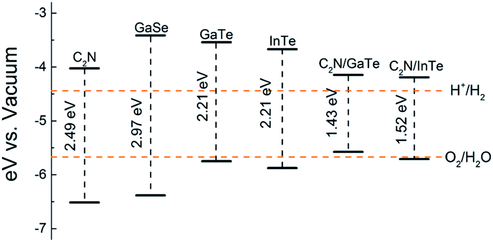 | ||
| Fig. 3 Band edge positions of isolated monolayers and heterojunctions. The redox potentials of water splitting are represented by orange dashed lines. | ||
Compared with the isolated monolayers, the band edge positions of the CBM and VBM in the heterojunctions are located closer to the redox potentials of water, suggesting higher photocatalytic efficiency and optical absorption.51 In order to investigate the optical absorption, the average absorption coefficients of x, y and z directions were calculated as shown in Fig. 4. Besides, the imaginary parts of the dielectric function are also shown in Fig. S5.† As shown in Fig. 4 and S5,† the C2N monolayer possesses absorption peaks in the visible spectrum while GaTe and InTe monolayers exhibit broad absorption in the near ultraviolet region. Fascinatingly, C2N/GaTe and C2N/InTe heterojunctions exhibit strong absorption in both visible and near ultraviolet regions with an intensity of 105 cm−1. Therefore, both the C2N/GaTe and C2N/InTe heterojunctions are efficient light harvesting photocatalysts.
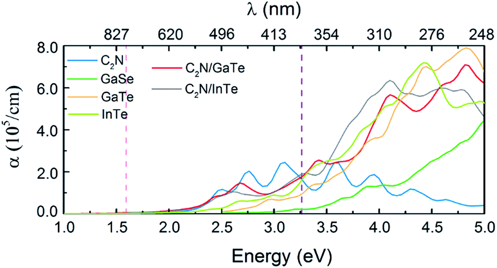 | ||
| Fig. 4 Optical absorption coefficients for the isolated C2N, GaSe, GaTe, and InTe monolayers as well as C2N/GaTe and C2N/InTe heterojunctions. The area between the red and the purple lines represents the visible-light range. | ||
Carrier mobility
The carrier mobility was investigated to further evaluate the photocatalytic performance of the heterojunctions. Generally, high carrier mobility could potentially improve the charge utilization for redox reactions before their recombination.25,52 Two directions of x and y were investigated as shown in Fig. S6.†The effective masses of electrons  and holes
  are computed by fitting parabolic functions to the CBM and VBM along the transport direction. The
  and
and  along the directions of x and y for the isolated C2N, GaTe and InTe monolayers as well as C2N/GaTe and C2N/InTe heterojunctions are shown in Tables S4† and 1. The
  of the C2N monolayer is much higher than the
  of C2N, indicating much lower hole mobility in the C2N monolayer, consistent with previous reports.25 For GaTe and InTe, the
  is also larger than
  , which agrees well with previously reported data,53,54 indicating the credibility of our results.
| |m*| | C | |E1| | μ 2D | ||
|---|---|---|---|---|---|
| C2N/GaTe | ex | 0.82 | 222.11 | 2.60 | 685.67 |
| hx | 1.06 | 222.11 | 1.55 | 1163.21 | |
| ey | 0.38 | 219.03 | 2.55 | 3229.29 | |
| hy | 0.86 | 219.03 | 1.82 | 1251.53 | |
| C2N/InTe | ex | 0.39 | 207.12 | 3.35 | 1744.56 |
| hx | 0.24 | 207.12 | 8.84 | 613.05 | |
| ey | 0.42 | 207.04 | 3.54 | 1330.34 | |
| hy | 0.31 | 207.04 | 8.88 | 390.98 |
To calculate the in-plane stiffness and DP constant, the relative energy and band edge positions of the CBM and VBM as a function of the uniaxial strain along the transport directions are shown in Fig. 5 and S7,† respectively. Based on the calculated effective masses, in-plane stiffness and DP constant, the carrier mobility of the isolated monolayers and heterojunctions could be obtained and are shown in Tables S4† and 1. In heterojunctions, the electron and hole mobility can become very high, which could be attributed to the improved in-plane stiffness and more dispersed valence band. The carrier mobility of C2N/GaTe and C2N/InTe is higher than that of many 2D semiconductors, such as MoS2 (ref. 38) and BN monolayers,55 and comparable to that of MXenes39 and phosphorene.56 The improved carrier mobility indicates that the transfer of carriers to reactive sites is easier during the photocatalytic process. Besides, due to the short distance for the photogenerated electrons and holes to migrate in 2D nanosheets, the recombination of photogenerated carriers is further reduced. Therefore, it can be inferred that the photocatalytic activity of the C2N/MX heterojunctions would be very good.
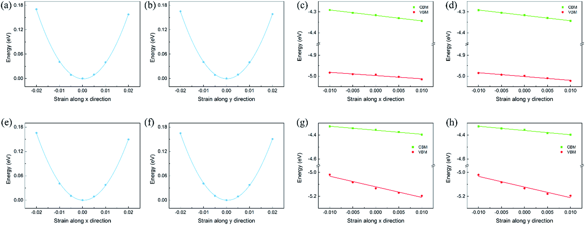 | ||
| Fig. 5 The relationship between energy and strain for (a, b) C2N/GaTe and (e, f) C2N/InTe. The CBM and VBM along the x and y directions as a function of deformation proportion for (c, d) C2N/GaTe and (g, h) C2N/InTe. | ||
To further evaluate the separation of the charge carrier, the exciton binding energies (Eb) were also calculated as shown in Table S5.† The Eb of C2N was calculated to be 1.24 eV, which is consistent with those in previous reports.25,57 C2N/GaTe and C2N/InTe exhibit much lower Eb values of 0.31 and 0.13 eV, respectively, indicating easier separation of carriers.
HER and OER catalytic activity
The HER and OER catalytic activity is critically important for overall water splitting photocatalysts. The HER performance was evaluated from ΔGH, which was widely used in previous reports.58–61 The OER catalytic activity was checked by using the free energy change of each step.62–65Since the CBM of C2N/GaTe and C2N/InTe heterojunctions is mainly contributed by C2N while the VBM mostly comes from the MX, the HER performance of the C2N layer and the OER catalytic activity of the MX layer were calculated. The ΔGH with different hydrogen coverages on the C2N layer is shown in Fig. 6.
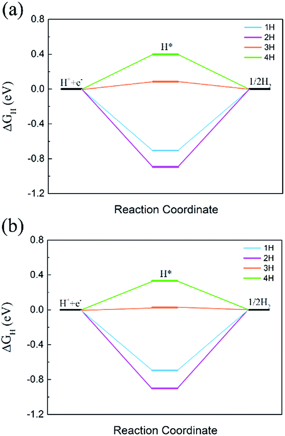 | ||
| Fig. 6 ΔGH with different hydrogen coverages on the C2N layer in (a) C2N/GaTe and (b) C2N/InTe heterojunctions. | ||
The ΔGH of the first two hydrogen atoms is too negative, indicating that the bonding is too strong. The ΔGH of the third hydrogen could reach 0.08 and 0.03 eV for C2N/GaTe and C2N/InTe, respectively, which are very close to zero, implying that C2N/GaTe and C2N/InTe are potentially excellent catalysts for the HER at an appropriate H coverage. The fourth hydrogen atom adsorbed on the C2N/GaTe and C2N/InTe heterojunctions would be close to the MX layer (Fig. S8†), leading to a positive ΔGH.
Then the OER performance of MX in the heterojunctions was investigated. In order to calculate the limiting step of the OER, the free energy of each elementary step (ΔG1 − ΔG4) was computed. The free energy diagrams of OER elementary steps on MX layers are shown in Fig. 7.
 | ||
| Fig. 7 Free energy diagram for the OER on MX in (a) C2N/GaTe and (b) C2N/InTe. | ||
For both C2N/GaTe and C2N/InTe heterojunctions, ΔG of the first three steps is positive while the last step is negative. The third step is the rate-limiting step with a ΔG of 2.70 and 2.17 eV for C2N/GaTe and C2N/InTe, respectively. At the standard reduction potential of water oxidation (1.23 eV), the ΔG of the rate-limiting step will decrease to 0.94 eV for C2N/InTe, which is comparable to and even lower than that of many TM@C catalysts or metal oxides.66
The stability of C2N in water has been experimentally confirmed24 while the MX has been proven to be stable by calculating their enthalpy of solvation.26 Therefore, the C2N/MX heterojunctions would be stable in water. Overall, both C2N/GaTe and C2N/InTe are type-II heterojunctions with strong absorption in both visible and near ultraviolet regions and high carrier mobility. Especially, C2N/InTe is a direct-band-gap heterojunction and exhibits excellent catalytic performance towards both the HER and the OER, indicating that it is a very promising photocatalyst for overall water splitting.
Conclusions
In conclusion, based on band edge positions and lattice parameters, we found that several kinds of MX monolayers can be used to fabricate type-II heterojunctions with C2N monolayers. By means of first-principles computations, we systematically investigated the photocatalytic performance of C2N/GaTe and C2N/InTe heterojunctions for overall water splitting. The results indicate that both are type-II heterojunctions, promoting the efficient spatial separation of electron–hole pairs; therefore, overcoming the electron–hole recombination issue. Interestingly, the C2N/InTe heterojunction exhibits a direct band gap. The band edge positions from the HSE06 functional predict that their band edges straddle water redox potentials, satisfying the requirements for photocatalytic water splitting. Besides, C2N/GaTe and C2N/InTe heterojunctions exhibit strong absorption in both visible and near ultraviolet regions. The calculations of carrier mobility illustrate that the heterojunctions possess higher carrier mobility compared with isolated monolayers, indicating that the transfer of charge carriers to the reactive sites is easier, reducing the probability of recombination of photogenerated carriers. The ΔGH can reach 0.08 and 0.03 eV for C2N/GaTe and C2N/InTe heterojunctions, respectively, leading to a high HER catalytic activity. Moreover, the C2N/InTe heterojunction possesses a good OER catalytic performance. These results indicate that C2N/GaTe and C2N/InTe heterojunctions, especially C2N/InTe, are very promising photocatalysts for water splitting. Our findings could be helpful to rationally design more type-II heterojunctions for photocatalytic water splitting.Conflicts of interest
There are no conflicts to declare.Acknowledgements
This work was supported by the National Natural Science Foundation of China (21421001). The computations were performed on the Magic Cube at the Shanghai Supercomputer Center.Notes and references
- X. Chen, S. Shen, L. Guo and S. S. Mao, Chem. Rev., 2010, 110, 6503–6570 CrossRef CAS PubMed.
- S. Y. Reece, J. A. Hamel, K. Sung, T. D. Jarvi, A. J. Esswein, J. J. H. Pijpers and D. G. Nocera, Science, 2011, 334, 645–648 CrossRef CAS PubMed.
- A. Fujishima and K. Honda, Nature, 1972, 238, 37–38 CrossRef CAS PubMed.
- A. Kudo and Y. Miseki, Chem. Soc. Rev., 2009, 38, 253–278 RSC.
- Y. Tachibana, L. Vayssieres and J. R. Durrant, Nat. Photonics, 2012, 6, 511–518 CrossRef CAS.
- J. Yang, D. Wang, H. Han and C. Li, Acc. Chem. Res., 2013, 46, 1900–1909 CrossRef CAS PubMed.
- M. Z. Rahman, K. Davey and S.-Z. Qiao, J. Mater. Chem. A, 2018, 6, 1305–1322 RSC.
- J. Ran, W. Guo, H. Wang, B. Zhu, J. Yu and S. Z. Qiao, Adv. Mater., 2018, 30, 1800128 CrossRef PubMed.
- J. Ran, B. Zhu and S. Z. Qiao, Angew. Chem., Int. Ed., 2017, 56, 10373–10377 CrossRef CAS PubMed.
- J. Ran, G. Gao, F.-T. Li, T.-Y. Ma, A. Du and S.-Z. Qiao, Nat. Commun., 2017, 8, 13907 CrossRef CAS PubMed.
- A. K. Singh, K. Mathew, H. L. Zhuang and R. G. Hennig, J. Phys. Chem. Lett., 2015, 6, 1087–1098 CrossRef CAS PubMed.
- X. Zhang, X. Zhao, D. Wu, Y. Jing and Z. Zhou, Adv. Sci., 2016, 3, 1600062 CrossRef PubMed.
- M. Zhou, X. W. Lou and Y. Xie, Nano Today, 2013, 8, 598–618 CrossRef CAS.
- D. Wu, X. Zhang, Y. Jing, X. Zhao and Z. Zhou, Nano Energy, 2016, 28, 390–396 CrossRef CAS.
- X. Zhang, Z. Zhang, D. Wu, X. Zhang, X. Zhao and Z. Zhou, Small Methods, 2018, 2, 1700359 CrossRef.
- X. Zhang, Z. Zhang, X. Zhao, D. Wu, X. Zhang and Z. Zhou, J. Mater. Chem. A, 2017, 5, 2870–2875 RSC.
- X. Wang, K. Maeda, A. Thomas, K. Takanabe, G. Xin, J. M. Carlsson, K. Domen and M. Antonietti, Nat. Mater., 2009, 8, 76–80 CrossRef CAS PubMed.
- T. A. Shifa, F. Wang, Z. Cheng, P. He, Y. Liu, C. Jiang, Z. Wang and J. He, Adv. Funct. Mater., 2018, 28, 1800548 CrossRef.
- Z. Cheng, T. A. Shifa, F. Wang, Y. Gao, P. He, K. Zhang, C. Jiang, Q. Liu and J. He, Adv. Mater., 2018, 1707433 CrossRef PubMed.
- H. Wang, L. Zhang, Z. Chen, J. Hu, S. Li, Z. Wang, J. Liu and X. Wang, Chem. Soc. Rev., 2014, 43, 5234–5244 RSC.
- S. J. A. Moniz, S. A. Shevlin, D. J. Martin, Z.-X. Guo and J. Tang, Energy Environ. Sci., 2015, 8, 731–759 RSC.
- J. Mahmood, E. K. Lee, M. Jung, D. Shin, I. Y. Jeon, S. M. Jung, H. J. Choi, J. M. Seo, S. Y. Bae, S. D. Sohn, N. Park, J. H. Oh, H. J. Shin and J. B. Baek, Nat. Commun., 2015, 6, 6486 CrossRef CAS PubMed.
- M. R. A. Kishore and P. Ravindran, ChemPhysChem, 2017, 18, 1526–1532 CrossRef CAS PubMed.
- L. Wang, X. Zheng, L. Chen, Y. Xiong and H. Xu, Angew. Chem., Int. Ed., 2018, 57, 3454–3458 CrossRef CAS PubMed.
- R. Kumar, D. Das and A. K. Singh, J. Catal., 2018, 359, 143–150 CrossRef CAS.
- H. L. Zhuang and R. G. Hennig, Chem. Mater., 2013, 25, 3232–3238 CrossRef CAS.
- G. Kresse and J. Furthmüller, Phys. Rev. B: Condens. Matter Mater. Phys., 1996, 54, 11169–11186 CrossRef CAS.
- G. Kresse and D. Joubert, Phys. Rev. B: Condens. Matter Mater. Phys., 1999, 59, 1758–1775 CrossRef CAS.
- J. P. Perdew, K. Burke and M. Ernzerhof, Phys. Rev. Lett., 1996, 77, 3865–3868 CrossRef CAS PubMed.
- S. Grimme, J. Antony, S. Ehrlich and H. Krieg, J. Chem. Phys., 2010, 132, 154104 CrossRef PubMed.
- S. Grimme, S. Ehrlich and L. Goerigk, J. Comput. Chem., 2011, 32, 1456–1465 CrossRef CAS PubMed.
- H. J. Monkhorst and J. D. Pack, Phys. Rev. B: Solid State, 1976, 13, 5188–5192 CrossRef.
- S. Kümmel and L. Kronik, Rev. Mod. Phys., 2008, 80, 3–60 CrossRef.
- J. Heyd, G. E. Scuseria and M. Ernzerhof, J. Chem. Phys., 2003, 118, 8207–8215 CrossRef CAS.
- J. Bardeen and W. Shockley, Phys. Rev., 1950, 80, 72–80 CrossRef CAS.
- M.-Q. Long, L. Tang, D. Wang, L. Wang and Z. Shuai, J. Am. Chem. Soc., 2009, 131, 17728–17729 CrossRef CAS PubMed.
- J. Qiao, X. Kong, Z.-X. Hu, F. Yang and W. Ji, Nat. Commun., 2014, 5, 4475 CrossRef CAS PubMed.
- Y. Cai, G. Zhang and Y.-W. Zhang, J. Am. Chem. Soc., 2014, 136, 6269–6275 CrossRef CAS PubMed.
- X. Zhang, X. Zhao, D. Wu, Y. Jing and Z. Zhou, Nanoscale, 2015, 7, 16020–16025 RSC.
- Y. Jing, X. Zhang, D. Wu, X. Zhao and Z. Zhou, J. Phys. Chem. Lett., 2015, 6, 4252–4258 CrossRef CAS PubMed.
- M. Gajdoš, K. Hummer, G. Kresse, J. Furthmüller and F. Bechstedt, Phys. Rev. B: Condens. Matter Mater. Phys., 2006, 73, 045112 CrossRef.
- H. H. Wu, Q. Meng, H. Huang, C. T. Liu and X. L. Wang, Phys. Chem. Chem. Phys., 2018, 20, 3608–3613 RSC.
- S. Saha, T. P. Sinha and A. Mookerjee, Phys. Rev. B: Condens. Matter Mater. Phys., 2000, 62, 8828–8834 CrossRef CAS.
- J. K. Nørskov, J. Rossmeisl, A. Logadottir, L. Lindqvist, J. R. Kitchin, T. Bligaard and H. Jónsson, J. Phys. Chem. B, 2004, 108, 17886–17892 CrossRef.
- Y.-A. Zhu, D. Chen, X.-G. Zhou and W.-K. Yuan, Catal. Today, 2009, 148, 260–267 CrossRef CAS.
- H. Wang, X. Li and J. Yang, ChemPhysChem, 2016, 17, 2100–2104 CrossRef CAS PubMed.
- T. Björkman, A. Gulans, A. V. Krasheninnikov and R. M. Nieminen, Phys. Rev. Lett., 2012, 108, 235502 CrossRef PubMed.
- Z. Liu, J. Z. Liu, Y. Cheng, Z. Li, L. Wang and Q. Zheng, Phys. Rev. B: Condens. Matter Mater. Phys., 2012, 85, 205418 CrossRef.
- S. Chen, L. Zuzhang, Z. Jian and S. Zhimei, 2D Mater., 2017, 4, 015027 Search PubMed.
- J. Wang, Z. Guan, J. Huang, Q. Li and J. Yang, J. Mater. Chem. A, 2014, 2, 7960–7966 RSC.
- W. Hu, L. Lin, R. Zhang, C. Yang and J. Yang, J. Am. Chem. Soc., 2017, 139, 15429–15436 CrossRef CAS PubMed.
- T. Luttrell, S. Halpegamage, J. Tao, A. Kramer, E. Sutter and M. Batzill, Sci. Rep., 2014, 4, 4043 CrossRef PubMed.
- L. Huang, Z. Chen and J. Li, RSC Adv., 2015, 5, 5788–5794 RSC.
- H. Jin, J. Li, Y. Dai and Y. Wei, Phys. Chem. Chem. Phys., 2017, 19, 4855–4860 RSC.
- S. Bruzzone and G. Fiori, Appl. Phys. Lett., 2011, 99, 222108 CrossRef.
- J. Qiao, X. Kong, Z. X. Hu, F. Yang and W. Ji, Nat. Commun., 2014, 5, 4475 CrossRef CAS PubMed.
- J. Sun, R. Zhang, X. Li and J. Yang, Appl. Phys. Lett., 2016, 109, 133108 CrossRef.
- C. Ling, L. Shi, Y. Ouyang and J. Wang, Chem. Mater., 2016, 28, 9026–9032 CrossRef CAS.
- G. Gao, A. P. O'Mullane and A. Du, ACS Catal., 2017, 7, 494–500 CrossRef CAS.
- G. Gao, S. Bottle and A. Du, Catal. Sci. Technol., 2018, 8, 996–1001 RSC.
- X. Zhang, A. Chen, Z. Zhang, M. Jiao and Z. Zhou, J. Mater. Chem. A, 2018, 6, 11446–11452 RSC.
- M. Li, L. Zhang, Q. Xu, J. Niu and Z. Xia, J. Catal., 2014, 314, 66–72 CrossRef CAS.
- C. Ling, L. Shi, Y. Ouyang, X. C. Zeng and J. Wang, Nano Lett., 2017, 17, 5133–5139 CrossRef CAS PubMed.
- G. Gao, E. R. Waclawik and A. Du, J. Catal., 2017, 352, 579–585 CrossRef CAS.
- Y.-N. Chen, X. Zhang, H. Cui, X. Zhang, Z. Xie, X.-G. Wang, M. Jiao and Z. Zhou, Energy Storage Materials, 2018, 15, 226–233 CrossRef.
- X. Cui, P. Ren, D. Deng, J. Deng and X. Bao, Energy Environ. Sci., 2016, 9, 123–129 RSC.
Footnote |
| † Electronic supplementary information (ESI) available. See DOI: 10.1039/c8na00084k |
| This journal is © The Royal Society of Chemistry 2019 |