DOI:
10.1039/C8NA00064F
(Communication)
Nanoscale Adv., 2019,
1, 64-70
MAPbI3 microneedle-arrays for perovskite photovoltaic application†
Received
28th June 2018
, Accepted 25th July 2018
First published on 17th August 2018
Abstract
Methyl-ammonium lead iodide perovskite (MAPbI3) was synthesized in the form of micro-needles via a hydrothermal route at a low temperature of 100 °C in a two-step procedure for the first time. The results exhibit that the amount of the surfactant is crucial for the synthesis of the MAPbI3 nanostructures with well-controlled morphologies. In contrast to bulk MAPbI3, the one-dimensional (1-D) micro-needle perovskite with a diameter of 200 nm showed an improved hole injection from the perovskite to the hole transporting layer (HTL), providing a unique platform at the perovskite/HTL interface. The best performing device employing MAPbI3 perovskite micro-needles yielded stable and hysteresis-free devices with a best power conversion efficiency of (PCEbest) of 17.98%. The current findings highlight the potential of perovskite micro-needles as novel absorber systems and lay the basis for future commercialization.
1. Introduction
Solar cells relying on lead organo-halide perovskite light absorbers have been widely investigated to produce economical solar cells due to their low-priced primary materials, opportunity to be fully solution-handled at low temperature and high-throughput fabrication on plastic and glass conducting substrates at a very low cost.1–3 The precise engineering of the light absorbing layer of perovskite solar cells (PSC) has recently resulted in remarkably efficient and stable devices demonstrating a power conversion efficiency (PCE) of 22.1% with iodide ministration in formamidinium-lead-halide-based perovskite absorber materials.4 In recent years, methyl ammonium lead iodide (MAPbI3) has been extensively studied with various morphologies (nanowires, nanofibers, and cuboids) owing to its key applications in light emitting diodes (LEDs)5,6 and high open-circuit-voltage (Voc) photovoltaic cells.7–9 Specifically, to achieve highly efficient and stable perovskite devices, MAPbI3 absorbing layers were fabricated by employing one and two-step spin coating, slot die coating, blade coating and spray coating techniques.10–14 Moreover, the crystallinity and morphology of these layers were further improved by the addition of an anti-solvent during the spin-coating process.15 During the spin-coating, the rapid crystallization of the perovskite absorber has been seen. Moreover, to achieve an optimized device efficiency, mostly a post-annealing treatment is needed. Furthermore, the highest photocurrents were obtained only with the highest perovskite surface coverage. Therefore, perovskite absorbing layers with compact, dense, pinhole free and well-aligned film structures are always desired in order to fabricate a highly efficient device.16,17
Usually, the transport of charges in a perovskite absorbing layer is subsequent to the charge separation at electron transporting material (ETM)/perovskite and perovskite/hole transporting layer (HTL) junctions. The separation of charges at the ETM/perovskite and perovskite/HTL junctions is badly affected and the probability of recombination of charges is enhanced though the carrier transport is not sufficient despite the carrier dissemination length reaching over 1 μm.18 It was also realized that the cell efficiency was mainly influenced by the carrier transport and recombination, where the recombination rate was swift within mesoscopic cells with no alteration in charge transport, which demonstrates that the perovskite absorber is mainly ruling the passages of charge transport.18 For the perovskite devices with the layer-by-layer configuration, the HTL/perovskite interfacial provision remains the same regardless of the device structure, indicating that there are problems in the course of charge separation at the HTL/perovskite junction.
To promote the hole migration from the perovskite absorber to the HTL and the subsequent separation at the HTL/perovskite junction, a one-dimensional (1-D) morphology like micro-needles of MAPbI3 is believed to be superior to a 3-D structure (nanocubes). 1-D nanowires of MAPbI3 have been investigated earlier by other researchers.15,19 However, nanowires were produced by different techniques and used in field emission transistors, which basically vary from photovoltaic cells.19 In the recent past, MAPbI3 nanowires were synthesized by a two-step spin-coating preparation technique and moderately efficient (PCE = 14.71%) PSCs based on these nanowires were fabricated.15 However, the described synthesis scheme is tedious with difficulty of operation, varying degrees of expenses and sophistication. To overcome these problems and to produce the state-of-the-art PSCs based on 1-D MAPbI3 morphologies, we report perovskite micro-needles grown by a low temperature solution processed hydrothermal method,20 followed by one-step spin coating. The hydrothermal process is a key method to produce perfectly controlled nanostructures with narrow-size distribution at lower temperature. We synthesize lead iodide (PbI2) micro-needles using a hydrothermal method in the presence of surfactant cetyltrimethylammonium bromide (CTAB) at a low temperature of 100 °C for 8 h.20 Surprisingly, MAPbI3 micro-needles were produced by covering the surface of PbI2 micro-needles using an isopropanol solution of CH3NH3I (MAI). To the best of our knowledge, no 1-D perovskite micro-needles have been reported to produce highly stable perovskite devices with a best PCE of 17.98% with no hysteresis.
2. Materials and methods
2.1. Fabrication of perovskite solar cells based on MAPbI3 micro-needles
Fluorine-doped tin-oxide (FTO) glass substrates were properly washed in an ultrasonic bath containing acetone followed by rinsing with ethanol and water for 20 min. The precursor solution was made by mixing 0.05 M zinc acetate dihydrate in ethanol![[thin space (1/6-em)]](https://www.rsc.org/images/entities/char_2009.gif) :water (30:70 v/v) solution. Primarily, a condensed layer of ZnO was formed onto the FTO glass via a spin coating route at 2500 rpm for 15 s and heated at 125 °C for 5 min. After that, a mesoporous layer of ZnO was deposited using an electrospray method under optimum film deposition conditions at a precursor spraying rate of 0.004 mL min−1, along a substrate to nozzle gap of 4.5 cm by employing a constant high voltage of 6.5 kV.21 The temperature of the hot plate was set at 150 °C to effectively evaporate the solvent during the entire process. PbI2 micro-needles were synthesized using the hydrothermal synthesis at a low temperature of 100 °C.20 To synthesize PbI2 micro-needles, one solution was prepared by dissolving 0.95 g of lead acetate (Pb(CH3CO2)2) in 10 mL of acetic acid and 0.04, 0.07 and 0.1 g of CTAB (to check the effect of the surfactant amount on the morphology) were also added to the same solution. Another solution was formed by dissolving 0.4193 g of potassium iodide (KI) in 5 mL of distilled water. After that, the solution of KI was poured drop-wise into the (Pb(CH3CO2)2) solution in acetic acid, using continuous magnetic stirring to produce a yellow-colored solution. By effective stirring for 10 min, 15 mL of deionized water (DI) were poured into the final solution and subsequently transferred into an autoclave and heated at 100 °C for 8 h to grow the PbI2 micro-needles. After cooling down the final product of PbI2 micro-needles, they were rinsed with distilled water to remove the residual salts and eventually dried at 60 °C for 4 h for further processing. Hydrothermally grown PbI2 micro-needles were further deposited as a layer by dissolving them in 1.5 mL of N,N-dimethylformamide (DMF) at 70 °C. After that, 20 μL of PbI2 micro-needle solution was poured onto the substrate surface and it was held for 10 s and then spin-coated at 3000 and 6000 rpm for 5 s, respectively. MAPbI3 micro-needles were formed by pouring a 200 μL MAI solution in isopropanol (35 mg:5 mL) with the addition of 50 μL of DMF and boarded on the PbI2 micro-needle layer for 40 s and spin-coated at 4000 rpm for 20 s followed by drying at 130 °C for 10 min. The HTL was deposited by spin coating 30 μL of spiro-OMeTAD (80 mg of 2,2′,7,7′-tetrakis(N,N-di-p-methoxyphenyl-amine)-9,9′-spirobifluorene, 8.4 μL of 4-tert-butylpyridine, and 51.6 μL of bis(trifluoromethane) sulfonamide lithium salt (Li-TFSI) solution (154 mg mL−1 in acetonitrile) in 1 mL chlorobenzene) solution for 10 s at 2000 rpm. Finally, a 90 nm thick top layer of Au was formed by thermal evaporation. For comparison, a perovskite absorber with a nanocubic morphology was obtained via a two-step sequential deposition method as described previously by us.22
:water (30:70 v/v) solution. Primarily, a condensed layer of ZnO was formed onto the FTO glass via a spin coating route at 2500 rpm for 15 s and heated at 125 °C for 5 min. After that, a mesoporous layer of ZnO was deposited using an electrospray method under optimum film deposition conditions at a precursor spraying rate of 0.004 mL min−1, along a substrate to nozzle gap of 4.5 cm by employing a constant high voltage of 6.5 kV.21 The temperature of the hot plate was set at 150 °C to effectively evaporate the solvent during the entire process. PbI2 micro-needles were synthesized using the hydrothermal synthesis at a low temperature of 100 °C.20 To synthesize PbI2 micro-needles, one solution was prepared by dissolving 0.95 g of lead acetate (Pb(CH3CO2)2) in 10 mL of acetic acid and 0.04, 0.07 and 0.1 g of CTAB (to check the effect of the surfactant amount on the morphology) were also added to the same solution. Another solution was formed by dissolving 0.4193 g of potassium iodide (KI) in 5 mL of distilled water. After that, the solution of KI was poured drop-wise into the (Pb(CH3CO2)2) solution in acetic acid, using continuous magnetic stirring to produce a yellow-colored solution. By effective stirring for 10 min, 15 mL of deionized water (DI) were poured into the final solution and subsequently transferred into an autoclave and heated at 100 °C for 8 h to grow the PbI2 micro-needles. After cooling down the final product of PbI2 micro-needles, they were rinsed with distilled water to remove the residual salts and eventually dried at 60 °C for 4 h for further processing. Hydrothermally grown PbI2 micro-needles were further deposited as a layer by dissolving them in 1.5 mL of N,N-dimethylformamide (DMF) at 70 °C. After that, 20 μL of PbI2 micro-needle solution was poured onto the substrate surface and it was held for 10 s and then spin-coated at 3000 and 6000 rpm for 5 s, respectively. MAPbI3 micro-needles were formed by pouring a 200 μL MAI solution in isopropanol (35 mg:5 mL) with the addition of 50 μL of DMF and boarded on the PbI2 micro-needle layer for 40 s and spin-coated at 4000 rpm for 20 s followed by drying at 130 °C for 10 min. The HTL was deposited by spin coating 30 μL of spiro-OMeTAD (80 mg of 2,2′,7,7′-tetrakis(N,N-di-p-methoxyphenyl-amine)-9,9′-spirobifluorene, 8.4 μL of 4-tert-butylpyridine, and 51.6 μL of bis(trifluoromethane) sulfonamide lithium salt (Li-TFSI) solution (154 mg mL−1 in acetonitrile) in 1 mL chlorobenzene) solution for 10 s at 2000 rpm. Finally, a 90 nm thick top layer of Au was formed by thermal evaporation. For comparison, a perovskite absorber with a nanocubic morphology was obtained via a two-step sequential deposition method as described previously by us.22
2.2. Characterization and cell performance measurements
The plane-view and cross-sectional nanostructures of perovskite devices were determined using a scanning electron microscope (SEM) (FE-SEM, JEOL, JSM-7600F). The phase formation of the ZnO and perovskite micro-needles was determined via X-ray diffraction (XRD) analysis (Macscience Instruments). The current-density vs. voltage plots (J–V curves) were measured using a Keithley model 2420 digital source meter (Keithley Instruments, Inc., USA) collected by using a solar simulator (solar AAA simulator, Oriel USA). Both the backward and forward voltage scans were performed with a rate of 10 mV/200 ms and a delay time of 200 ms.
3. Results and discussion
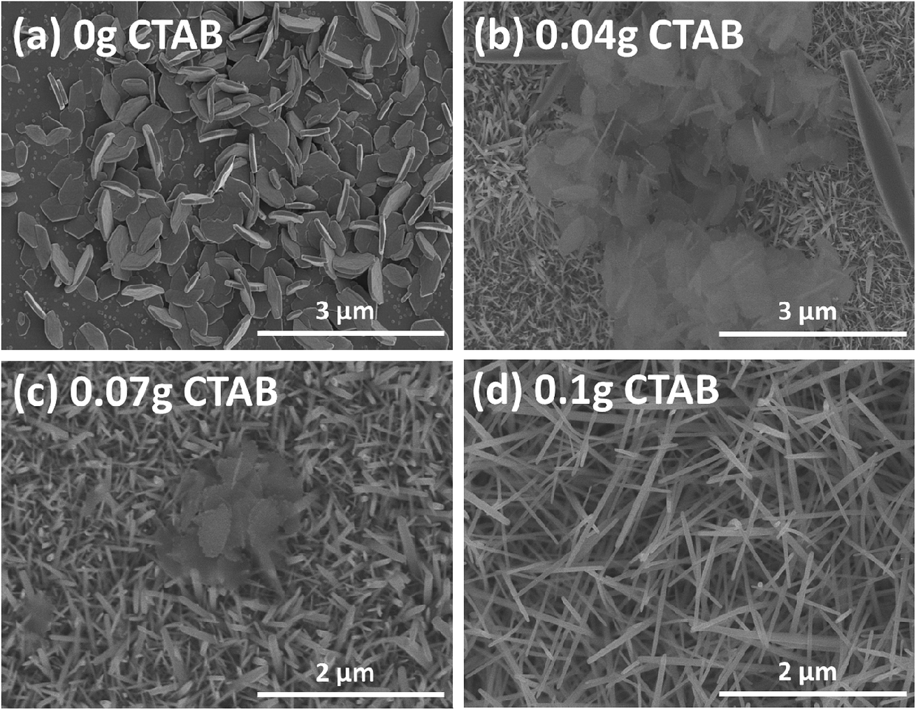
Fig. 1 shows the plane-view SEM micrographs of PbI2 micro-needles grown using a hydrothermal route with different amounts of surfactant CTAB. The SEM micrographs showed that the quantity of CTAB in the growth solution have a significant influence on the PbI2 micro-needle morphology. By altering the CTAB amount in the synthesis solution, PbI2 with various nanostructures can be grown properly as observed in Fig. 1. Without the addition of CTAB to the synthesis solution, micro-flakes of PbI2 were observed (Fig. 1a). As seen in Fig. 1b, the PbI2 layer synthesized at a low CTAB concentration of 0.04 g consists mainly of PbI2 micro-needles (having diameters in the range of 600–800 nm) with sparse PbI2 micro-flakes. By further increasing the amount of CTAB to 0.07 g, we observe mainly PbI2 micro-needles with a diameter of about 400–500 nm (Fig. 1c). When the amount of CTAB was further increased to 0.1 g, PbI2 micro-needles (with a diameter of about 200 nm) were completely grown without flakes (Fig. 1d), which helps the MAI solution to infiltrate and completely convert PbI2 micro-needles into MAPbI3 micro-needles demonstrating positive consequences on the performance of solar cells. Furthermore, Fig. S1† clearly exhibits the low magnification SEM image which confirms the uniformity of PbI2 micro-needles over a large scale.
 |
| | Fig. 1 Plane-view SEM micrographs of the PbI2 micro-needles synthesized by the hydrothermal route with various amounts of CTAB: 0 g (a), 0.04 g (b), 0.07 g (c), and 0.10 g (d), respectively. | |
A magnified view of PbI2 micro-needles is shown in Fig. 2a. A dense web of PbI2 micro-needles is formed and grown at some angle to the FTO substrate surface describing the porous nature of the micro-needles. The porous nature of the micro-needles is very important because the HTL will be diffused into these pores. The cubic morphology of the perovskite absorber formed by the two-step sequential deposition method can be clearly seen in Fig. 2b. A magnified view of these cubes is also exhibited in Fig. 2c, where the mesoporous ZnO surface was partially covered with MAPbI3 cubes in contrast to the MAPbI3 micro-needles covering the entire surface of the substrate (Fig. 2d). The MAPbI3 cube film does not have a smooth surface rather the MAPbI3 cubes are embedded in the film and grown apart from each other and hence, the surface coverage is very poor. On the other hand, after pouring a typical MAI solution in isopropanol (IPA) along with a limited amount of DMF in it, the PbI2 micro-needles (Fig. 2a) are completely converted to MAPbI3 micro-needles as shown in Fig. 2d. The MAPbI3 micro-needle film has a smooth surface and complete coverage over the mesoporous ZnO layer which is beneficial for the performance enhancement of perovskite solar cells. In addition, in Fig. 2e and f we show the side-view SEM image of the cells with the structure of FTO glass/condensed ZnO layer/MAPbI3 cubes and MAPbI3 micro-needle layers, respectively. In the case of MAPbI3 micro-needles, the layers are well-connected (Fig. 2f), while a gap can be seen between the surface of the MAPbI3 cubes and ZnO compact film, which causes an imbalance in charge transport and hysteresis at the ZnO/MAPbI3 interface.23 The side-view SEM micrograph of the complete device with a typical structure of FTO glass substrate/ZnO condensed layer/ZnO mesoporous film/MAPbI3 micro-needles/HTL/Au is shown in Fig. S2.† All the interfaces are well connected with no voids between them, indicative of complete pore filling of PbI2 micro-needles with the MAI. Moreover, a uniform coverage of perovskite micro-needles covered with spiro-MeOTAD as the HTL is also seen demonstrating the complete separation of charges at the HTL/perovskite junction. In Fig. S3,† a comparison of X-ray diffraction (XRD) spectra of the devices with perovskite cubes and micro-needles is shown. Both patterns exhibit an intense diffraction peak at 14.08°, which confirms the formation of a tetragonal structured perovskite.23 We observe strong peak intensities for the perovskite needle based cell demonstrating the better morphology and high crystallinity of the perovskite needles compared to the perovskite cubes.
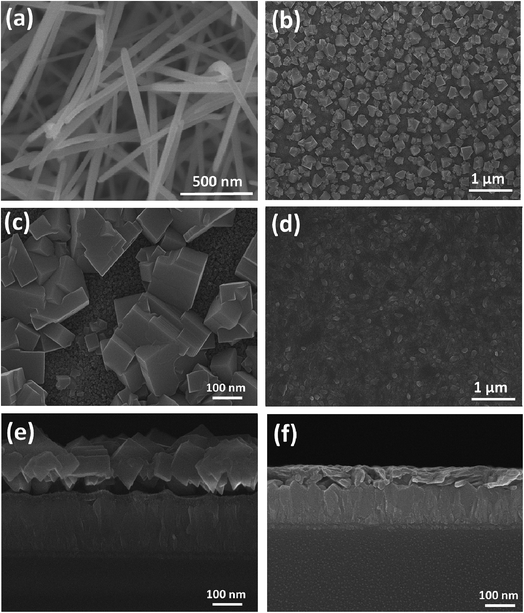 |
| | Fig. 2 Plane-view SEM micrographs showing (a) a magnified view of PbI2 micro-needles and (b) nano-cubes of the perovskite, (c) a magnified view of perovskite nano-cubes and (d) MAPbI3 micro-needles, and cross-sectional SEM images of FTO glass substrate/ZnO compact layer/(e) perovskite nano-cubes and (f) MAPbI3 micro-needles, respectively. | |
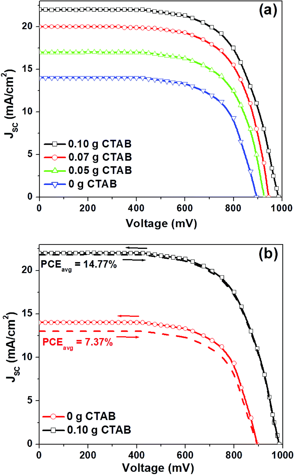
Next, we have fabricated a perovskite solar cell based on MAPbI3 micro-needles. Fig. 3a presents the current density–voltage (J–V) plots (in the reverse direction only) of the perovskite solar cells as a function of CTAB concentrations. The photovoltaic parameters such as short-circuit-current density (JSC), fill factor (FF), open-circuit-voltage (Voc) and power conversion efficiency (PCE) for the analogous devices are outlined in Table 1. As the amount of CTAB in the synthesis solution increases from 0 g to 0.10 g, JSC exhibits an increasing trend, approaching a value of 22.0 mA cm−2 from 14.0 mA cm−2. Moreover, when the amount increases from 0 g to 0.10 g, Voc rises from 895 mV to 985 mV and the PCE improves from 7.64% to 14.73%. The significant improvements in the device efficiency can be interpreted based on SEM findings: in the case of a 0.1 g CTAB amount in the synthesis solution, the density of MAPbI3 micro-needles is high enough to acquire a larger surface area between the ZnO mesoporous layer and the HTL allowing a good penetration of the MAI into PbI2 micro-needles (Fig. 1d). Furthermore, with the better MAI penetration and better contact with the ZnO mesoporous film, the transfer of electrons to the ZnO becomes extra energetic, ensuring the enhancement of JSC. Also, maintaining a better contact with the HTL, the PCE is overall enhanced caused by complete charge separation at the HTL/perovskite interface. We consider that this might be due to the decreasing gaps between MAPbI3 micro-needles in the presence of MAPbI3 nano-flakes (Fig. 1a–c), which can inhibit the full penetration of the MAI and decrease the effective surface area between the perovskite and the HTL and thus, results in extra charge recombination. We have also obtained the J–V plots (both in the reverse and forward voltage sweeps) for the cells with 0 g and 0.1 g CTAB concentrations (Fig. 3b). An average power conversion efficiency (PCEavg) of 7.37% to 14.77% was obtained for these devices, respectively. The devices made with 0.1 g CTAB concentration showed a hysteresis-less behavior with nominal alteration in the value of JSC. The hysteresis-less behavior for the 0.1 g CTAB case is attributed to the better morphology and contact between the MAPbI3 micro-needles and HTL facilitating the charge separation at the HTL/perovskite interface. The statistics of PCE at different CTAB concentrations is shown in Fig. S4.†
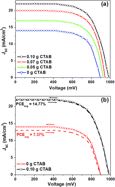 |
| | Fig. 3 Typical J–V plots of various micro-needle perovskite solar cells (a) as a function of CTAB concentration (in the reverse direction only), and (b) based on 0 g and 0.1 g CTAB concentration, in different scanning directions, respectively. | |
Table 1 Typical photovoltaic parameters obtained from the J–V measurements for perovskite devices as a function of CTAB concentration in the synthesis solution (error bars were obtained for 20 devices)
| CTAB concentration (g) |
V
oc (mV) |
FF (%) |
J
SC (mA cm−2) |
PCE (%) |
| 0 |
895 ± 1.3 |
61 ± 2.2 |
14 ± 0.51 |
7.64 ± 0.41 |
| 0.04 |
925 ± 2.3 |
62 ± 1.4 |
17 ± 0.50 |
9.74 ± 0.38 |
| 0.07 |
945 ± 2.2 |
63 ± 2.3 |
20 ± 0.60 |
11.90 ± 0.33 |
| 0.10 |
990 ± 1.1 |
68 ± 1.4 |
22 ± 0.30 |
14.81 ± 0.28 |
The comparison of J–V plots (in different scanning directions) of the perovskite solar cells based on MAPbI3 micro-needles (grown at 0.1 g CTAB concentration) and MAPbI3 nano-cubes is presented in Fig. 4a and the photovoltaic parameters are summarized in Table 2. Clearly, the MAPbI3 micro-needle based devices demonstrate a significantly higher PCEavg (14.77%) compared to the cells with the perovskite nano-cube morphology (PCEavg of 10.48%), thanks to the well-connected interfaces and efficient separation of charges at the perovskite and HTL interface. Most importantly, the hysteresis (calculated here as the difference between the PCE values of the reverse and forward scanning directions) varied significantly for both the cases as plotted in Fig. 4b. The devices based on MAPbI3 micro-needles showed no difference between the forward and reverse scans, whereas the nano-cubes of MAPbI3 revealed more hysteresis. The lowest values of hysteresis depend mainly on the interfacial engineering of the cells by growing the MAPbI3 micro-needles and the better contact between the interfaces.
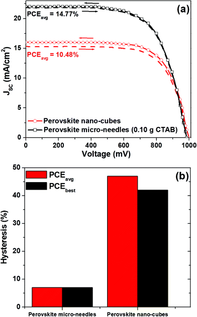 |
| | Fig. 4 (a) Comparison of J–V plots of perovskite devices based on MAPbI3 micro-needles and nano-cubes, and (b) hysteresis for devices with MAPbI3 micro-needles and nano-cubes, respectively. | |
Table 2 Photovoltaic parameters (in different scanning directions) for devices with MAPbI3 micro-needles and nano-cubes, under one sun illumination (AM 1.5G, 100 mW cm−2)
| Perovskite morphology |
Scan direction |
J
SC (mA cm−2) |
V
oc (mV) |
FF (%) |
PCEavg (%) |
PCEmax (%) |
| MAPbI3 micro-needles |
Reverse |
22.0 |
990 |
68 |
14.81 ± 0.10 |
18.02 |
| Forward |
21.90 |
990 |
68 |
14.74 ± 0.11 |
17.95 |
| Average |
21.95 |
990 |
68 |
14.77 ± 0.11 |
17.98 |
| MAPbI3 nano-cubes |
Reverse |
16.0 |
1000 |
67 |
10.72 ± 0.13 |
12.54 |
| Forward |
15.30 |
1000 |
67 |
10.25 ± 0.11 |
12.12 |
| Average |
15.65 |
1000 |
67 |
10.48 ± 0.12 |
12.48 |
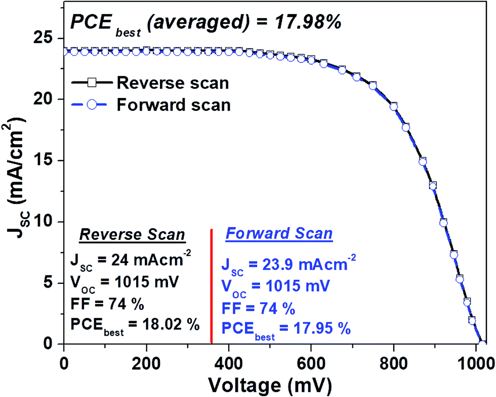
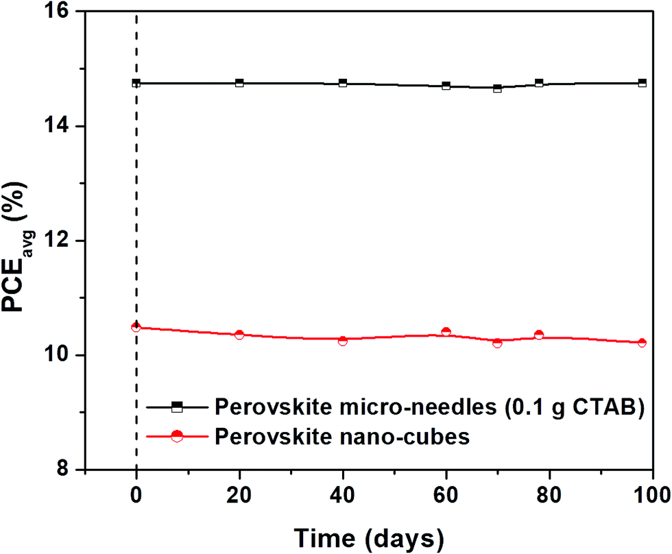
The J–V plots of the best devices based on MAPbI3 micro-needles both in the reverse and forward scans are plotted in Fig. 5. The best cells demonstrate a PCEbest (averaged) of 17.98% with no hysteresis, the highest efficiency values reported for 1-D perovskite micro-needle based cells. Moreover, the cell stability (stored in dry air) is recorded systematically, revealing excellent stability, with MAPbI3 micro-needle devices maintaining over 14.77% PCE even after 100 days (Fig. 6). On the other hand, slight variations in PCEs are observed for the cells based on perovskite nano-cubes.
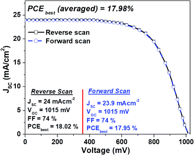 |
| | Fig. 5
J–V curves (both in the forward and reverse scans) for the best-performing device with MAPbI3 micro-needles. | |
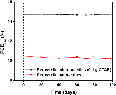 |
| | Fig. 6 Long-term stability test of un-encapsulated devices based on MAPbI3 micro-needles and perovskite nano-cubes stored in dry air. | |
4. Conclusion
Highly crystalline MAPbI3 micro-needles were successfully formed by a two-step low-temperature hydrothermal method and employed in perovskite devices yielding a best PCE of 17.98% for the first time ever. In contrast to the nano-cubes of MAPbI3, the injection of holes from the perovskite to the HTL was enhanced for the micro-needle morphology, which provides a substantial new understanding of engineering at the perovskite/HTL junction. MAPbI3 micro-needles provide a best platform for fabricating a pin-hole free perovskite solar cell with a better morphology and crystallinity.
Conflicts of interest
There are no conflicts to declare.
Acknowledgements
The authors gratefully acknowledge the financial support from the Higher Education Commission (HEC) of Pakistan.
References
- K. Mahmood, S. Sarwar and M. T. Mehran, RSC Adv., 2017, 7, 17044–17062 RSC.
- N.-G. Park, M. Grätzel, T. Miyasaka and K. Zhu, Nat. Energy, 2016, 1, 16152 CrossRef CAS.
- K. Mahmood, B. S. Swain and A. Amassian, Adv. Mater., 2015, 27, 2859–2865 CrossRef CAS PubMed.
- W. S. Yang, B. W. Park, E. H. Jung, N. J. Jeon, Y. C. Kim, D. U. Lee, S. S. Shin, J. Seo, E. K. Kim, J. H. Noh and S. I. Seok, Science, 2017, 356, 1376–1379 CrossRef CAS PubMed.
- H. Cho, S. H. Jeong, M. H. Park, Y. H. Kim, C. Wolf, C. L. Lee, J. H. Heo, A. Sadhanala, N. Myoung, S. Yoo, S. H. Im, R. H. Friend and T. W. Lee, Science, 2015, 350, 1222 CrossRef CAS PubMed.
- Z. Xiao, R. A. Kerner, L. Zhao, N. L. Tran, K. M. Lee, T. W. Koh, G. D. Scholes and B. P. Rand, Nat. Photonics, 2017, 11, 108 CrossRef CAS.
- J. H. Noh, S. H. Im, J. H. Heo, T. N. Mandal and S. I. Seok, Nano Lett., 2013, 13, 1764–1769 CrossRef CAS PubMed.
- S. Aharon, B. E. Cohen and L. Etgar, J. Phys. Chem. C, 2014, 118, 17160–17165 CrossRef CAS.
- K. Mahmood, B. S. Swain and A. Amassian, Adv. Energy Mater., 2015, 5, 1500568 CrossRef.
- K. Mahmood, B. S. Swain, A. R. Kirmani and A. Amassian, J. Mater. Chem. A, 2015, 3, 9051–9057 RSC.
- J. Luo, Y. Wang and Q. Zhang, Sol. Energy, 2018, 163, 289–306 CrossRef CAS.
- M. Remeika, S. R. Raga, S. Zhanga and Y. Qi, J. Mater. Chem. A, 2017, 5, 5709–5718 RSC.
- Y. Zhong, R. Munir, J. Li, M. C. Tang, M. R. Niazi, D. M. Smilgies, K. Zhao and A. Amassian, ACS Energy Lett., 2018, 3, 1078–1085 CrossRef CAS.
- D. Lee, Y.-S. Jung, Y.-J. Heo, S. Lee, K. Hwang, Y.-J. Jeon, J.-E. Kim, J. Park, G. Y. Jung and D.-Y. Kim, ACS Appl. Mater. Interfaces, 2018, 10, 16133–16139 CrossRef CAS PubMed.
- J.-H. Im, J. Luo, M. Franckevičius, N. Pellet, P. Gao, T. Moehl, S. M. Zakeeruddin, M. K. Nazeeruddin, M. Grätzel and N.-G. Park, Nano Lett., 2015, 15, 2120–2126 CrossRef CAS PubMed.
- J.-H. Im, I. H. Jang, N. Pellet, M. Grätzel and N.-G. Park, Nat. Nanotechnol., 2014, 9, 927 CrossRef CAS PubMed.
- H. S. Ko, J. W. Lee and N. G. Park, J. Mater. Chem. A, 2015, 3, 8808 RSC.
- V. Gonzalez-Pedro, E. J. Juarez-Perez, W.-S. Arsyad, E. M. Barea, F. Fabregat-Santiago, I. Mora-Sero and J. Bisquert, Nano Lett., 2014, 14, 888–893 CrossRef CAS PubMed.
- E. Horváth, M. Spina, Z. Szekrényes, K. Kamarás, R. Gaal, D. Gachet and L. Forró, Nano Lett., 2014, 14, 6761–6766 CrossRef PubMed.
- G. Zhu, P. Liu, M. Hojamberdiev, J.-P. Zhou, X. Huang, B. Feng and R. Yang, Appl. Phys. A, 2010, 98, 299–304 CrossRef CAS.
- K. Mahmood, B. S. Swain and H. S. Jung, Nanoscale, 2014, 6, 9127–9138 RSC.
- K. Mahmood and A. Khalid, Mater. Lett., 2018, 224, 78–81 CrossRef CAS.
- X. Zheng, B. Chen, M. Yang, C. Wu, B. Orler, R. B. Moore, K. Zhu and S. Priya, ACS Energy Lett., 2016, 1, 424 CrossRef CAS.
Footnote |
| † Electronic supplementary information (ESI) available. See DOI: 10.1039/c8na00064f |
|
| This journal is © The Royal Society of Chemistry 2019 |
Click here to see how this site uses Cookies. View our privacy policy here. 
 Open Access Article
 This Open Access Article is licensed under a Creative Commons Attribution-Non Commercial 3.0 Unported Licence
 *a,
Arshi
Khalid
b and
Muhammad Taqi
Mehran
c
*a,
Arshi
Khalid
b and
Muhammad Taqi
Mehran
c