
 Open Access Article
 This Open Access Article is licensed under a Creative Commons Attribution-Non Commercial 3.0 Unported Licence
The surface hybridization of diamond with vertical graphene: a new route to diamond electronics†
K. P. S. S.
Hembram‡
a,
Sohyung
Lee‡
ab,
Hyunsik
Im
 b,
Hyunsu
Ju
a,
Sang-Hun
Jeong
c and
Jae-Kap
Lee
*a
b,
Hyunsu
Ju
a,
Sang-Hun
Jeong
c and
Jae-Kap
Lee
*a
aCenter for Opto-electronic Materials and Devices, Korea Institute of Science and Technology (KIST), Seoul, 02792, South Korea. E-mail: jklee@kist.re.kr
bDepartment of Semiconductor Science, Dongguk University, Seoul 04620, South Korea
cGwangju Center, Korea Basic Science Institute (KBSI), Gwangju 61186, South Korea
First published on 14th November 2019
Abstract
Herein a method is proposed for engineering the electronic properties (including the band structure) of diamond via surface hybridization with graphene. Graphene layers (5–50 nm in thickness) were grown vertically onto a polished 〈110〉 textured polycrystalline diamond plate (1 × 1 cm2) (vGr-diamond) at ∼1300 °C via hydrogen plasma etching in a chemical vapor deposition (CVD) chamber. Due to the crystallographic relationship, the graphene layers embed at an angle of 30° to the diamond surface comprising the (110) planes. The epitaxial relationship is demonstrated via low angle X-ray diffraction (XRD), the XRD rocking curve, Raman and scanning electron microscopy. With hybridization, the diamond sample reveals a strong photoluminescent (PL) signal at ∼2.78 eV (∼450 nm). The peak was assigned to the ‘interface defects’ of the vGr-diamond hybrid structure, which are a type of ‘surface defect’ of the CVD diamond that generates a peak at ∼2.69 eV. The blue shift (∼90 meV) of the interface defects is due to the compressive strain of ∼3% applied to the interface atoms. Simulations indicate that the hybrid structures possess a finite band gap of 1.85–0.25 eV, which decreases upon increasing the thickness of the graphene layers to ∼1.4 nm. The appearance of a small band gap was attributed to the compressive strain. These findings may provide a route for diamond to become a platform for next generation and extreme electronic devices.
New conceptsThe successful synthesis of diamond via chemical vapor deposition (CVD) in the 1980s has launched the quest to create diamond electronics. The progress has been delayed, and recently its potential seems to be decreasing. This is due to not only the limitation of the deposition area for single crystal diamond plates, but also to the difficulty in doping boron or nitrogen, which tends to degrade the crystallinity of the diamond. Here, a method to engineer the band gap of diamond via hybridization with graphene is reported. Vertical graphene nanolayers have been grown on a polished 〈110〉 textured polycrystalline diamond plate (1 × 1 cm2) (vGr-diamond) via hydrogen plasma treatment using a conventional plasma CVD process. Graphene planes are formed at an angle of 30° to the diamond surface comprising (110) planes. A new electronic transition at ∼2.78 eV due to ‘interface defects’ of the vGr-diamond hybrid structure is demonstrated using photoluminescence measurements. The interface defects also produce a compressive strain of ∼3%, enabling the band gap of the diamond to be changed. Simulations indicate that the hybrid structures possess a finite band gap of 1.85–0.25 eV, which decreases upon an increase in the thickness of the graphene layers up to ∼1.4 nm. The approach provides a new route for the creation of diamond electronics. |
The exploration of diamond electronics,1,2 launched with the successful synthesis of diamond by chemical vapor deposition (CVD)3,4 in the 1980s, is still challenging. This is due to not only the limitation of the deposition area (∼1 × 1 cm2) for single crystal diamond plates,4,5 but also to the difficulty in band gap engineering.6,7 Doping an impurity is an ideal way to band gap engineer a semiconducting material and this has opened up the use of silicon in the current era. For diamond with a wide band gap of 5.47 eV, however, the doping approach revealed difficulty in controlling the dopants as well as degradation of crystallinity with heavy doping of boron or nitrogen.6 The latter problem is more radical because it is due to a change of gas chemistry during the in situ doping. Boron and nitrogen doping through implantation increases the conductance of diamond.8,9 However, its availability for band gap engineering is unclear although the improved conduction can be attributed to the reduction of band gap. With the recent progress on synthesis of 2D materials including graphene, structural hybridization has been suggested as a feasible way to use band gap engineering for novel materials.10–14 For instance, the lateral hetero structure of hexagonal boron nitride (h-BN) (insulating) with graphene (semi-metallic) tunes the band gap of h-BN or graphene.10–17
Lambrecht et al. suggested direct nucleation of diamond on the edges of graphite (graphene layers) where the epitaxial relationship was expected to be diamond (110) planes and graphene layers.18 Similar epitaxial growth of graphene on diamond has been demonstrated by Lee et al.19 and Tulic et al.,20 separately, using conventional CVD. Graphene anchors vertically on the diamond interface (111) plane as well as forming connections with numerous diamond internal (111) planes, based on 1![[thin space (1/6-em)]](https://www.rsc.org/images/entities/char_2009.gif) :1 and 2:1 registries (Fig. S1, ESI†).19 Herein, the hybrid structure is synthesized where graphene planes are vertically formed on polished 〈110〉 textured diamond plates by using a high-temperature (∼1300 °C) plasma treatment using a direct current plasma CVD process,21 and show the feasibility for band gap engineering of the vertical (v) graphene-diamond (vGr-diamond) hybrid structure.
:1 and 2:1 registries (Fig. S1, ESI†).19 Herein, the hybrid structure is synthesized where graphene planes are vertically formed on polished 〈110〉 textured diamond plates by using a high-temperature (∼1300 °C) plasma treatment using a direct current plasma CVD process,21 and show the feasibility for band gap engineering of the vertical (v) graphene-diamond (vGr-diamond) hybrid structure.
The graphene layers in the hybrid structure with the 1:1 and 2:1 registry (this is simply defined as a 5:3 registry, i.e., five diamond (111) planes for three graphene layers) are positioned with the interlayer distances of 2.19 Å and 4.36 Å, respectively, at the diamond interface (111) plane, and normalize to 3.75 Å at their free end (Fig. 1a) to maintain an equilibrium in the van der Waals force. The interface reveals two typical configurations according to whether the diamond internal (111) plane at the interface is connected to graphene, or disconnected (Fig. 1a and f–h). The former forms a hybrid structure by anchoring graphene, but are strained producing three dissimilar hexagonal motifs (Fig. 1b). The motif at the interface reveals a bond length of 1.51 Å between C1 (sp2) and C2 (sp3) whereas those on the diamond and graphene sides retain their respective bond lengths of 1.54 Å and 1.42 Å. Appearance of the unique bond length of 1.51 Å is due to a σ bond from the sp2 and sp3 orbitals. It possesses 33% s-character (sp2) from the graphene side and 25% s-character (sp3) from the diamond side. Hence, it is stronger than the C–C (sp3–sp3) σ bond of diamond and weaker than the C–C (sp2–sp2) σ bond of graphene. Moreover, the motif at the interface is pseudo-planar, possessing various bond angles ranging from 106° to 115°. The pseudo-planar structure and dissimilar bond angles are due to bending of the graphene planes at the interface to retain a graphite-like planar structure. These features are attributed to the steric effect, accomplished from both of the sides. Away from the interface the σ bonds are due to two similar sp3 (sp2) orbitals. However, the atoms on the disconnected diamond internal (111) plane minimize strain with hydrogenation (Fig. 1a).
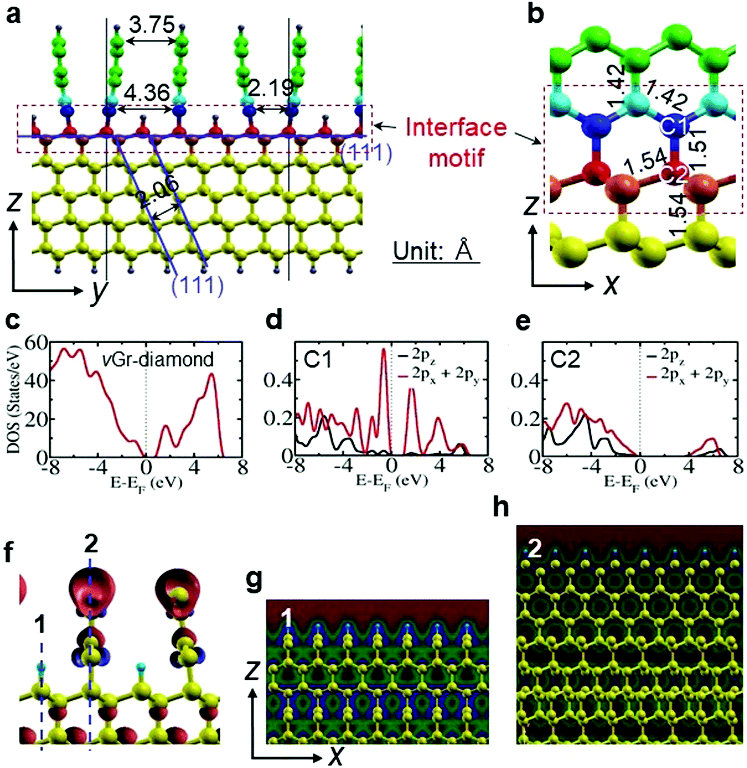 | ||
| Fig. 1 Atomic models and electronic structures of vGr-diamond. (a) The hybrid structure of diamond-graphene with a 5:3 registry (front view). The end dangling bonds on the top of the diamond (111) plane are saturated with hydrogen atoms. (b) A zoomed-in model (side view of the model). The numbers indicate the carbon–carbon bond lengths in angstrom units. (c) The total electronic DOS of the hybrid structure. (d and e) The partial electronic DOS of C1 and C2 carbon atoms at the interface motif. (f) The spin density at the interface. (g and h) Iso-charge contour plots for the planes of line 1 and 2 in (f), revealing the distribution of electrons, which are localized on the diamond side (g), but delocalized on the graphene side (h). | ||
A density of states (DOS) simulation shows that the vGr-diamond hybrid structure shown in Fig. 1c opens a band gap of ∼1.00 eV. The C1 and C2 atoms at the interface show a difference in their partial electronic DOS (Fig. 1d and e). There is a finite electron density from the 2px + 2py orbitals near the Fermi level in the valence band for the C1 atom, whereas the electron density is less for the C2 atom. The electronic states in the conduction bands are ∼1.20 eV and ∼4.00 eV above the valence bands for C1 and C2 atom, respectively. With a small energy excitation, the electrons in the graphene side can easily move to the conduction band. The electron spin density (Fig. 1f) indicates that the vacant 2pz orbital is available for conduction of free electrons in the graphene side.
Hybridization of the vGr-diamond is performed by exposing the surface of the polished diamond plate to hydrogen plasma at 1300 °C (pressure 100 Torr) where graphite is kinetically stable in the CVD condition (diamond is stable at 800–1100 °C).4 Formation of a graphitic phase on the polished diamond plate is evident in the optical microscopy image which is different from that of the bare mirror polished polycrystalline diamond plate shown in Fig. 2a. The photograph was taken with the reflection of a light by tilting the sample to show the difference clearly. The scanning electron microscopy (SEM) image reveals a localized pattern (Fig. 2b). The graphene layers are stable in ultrasonic mixing in alcohol.
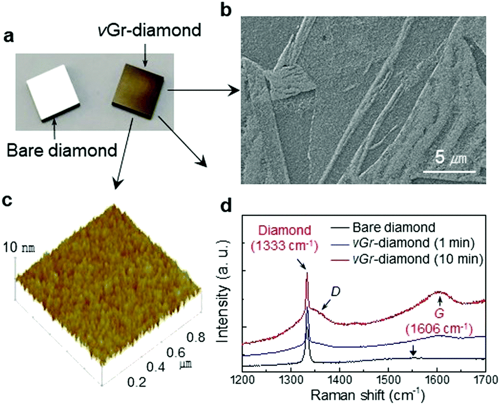 | ||
| Fig. 2 Analysis of the vGr-diamond hybrid structures. (a) Optical microscopy images of the bare diamond and hybrid structure diamond plates (1 × 1 cm2) which are cut from a diamond wafer 4 inches in diameter.21 (b) An SEM image of the hybrid structure. (c) An AFM image of the hybrid structure. The root mean square (RMS) value was ∼3 nm. (d) Raman spectra measured from the samples. The arrow on the Raman spectrum of bare diamond indicates a broad signal (∼1550 cm−1) for sp2 related defects in the CVD diamond. | ||
The AFM analysis for the surface of the hybrid structure (etched for 1 min) indicates the uniform growth of the graphene layers (Fig. 2c) where thickness is expected to be ∼5 nm (Fig. S2, ESI†). The Raman spectrum measured from the graphene side of the vGr-diamond hybrid structures revealed D (∼1360 cm−1) and G (1606 cm−1) peaks whereas bare diamond revealed a broad signal at ∼1550 cm−1 (arrow on the spectrum) due to the sp2 in diamond which is unique to a freestanding CVD diamond (Fig. 2d). It was expected that the 1606 cm−1 peak is shifted from ∼1582 cm−1 for graphite22 (the graphene layers can be regarded as graphite epitaxially grown on diamond) due to the unique 1.51 Å bond length (Fig. 1b). The shift (corresponding to a stress level of ∼7 GPa23) was attributed to the unique 1.51 Å bond length (8.45% longer than 1.42 Å for sp2) rather than the real stress applied to the sample. Thus, the unique 1606 cm−1 peak becomes ‘Raman evidence’ for the hybrid structure. Here, it is expected that the narrower spacing (2.19 Å) of the parallel graphene layers with the 1:1 registry (Fig. 1a) may contribute to the shift of the G peak. Almost no shift of the 1333 cm−1 peak for diamond (1332 cm−1 for natural diamond)22,24 was observed. This indicated that the diamond matrix was free from stress which was also supported by the HRTEM images which revealed well-ordered lattices.19,20
With the structural similarity of diamond (111) and graphene (see Fig. 3a and b) and the role of atomic hydrogen on the kinetics (stability) of diamond in a CVD condition,4 a formation mechanism of the hybrid structures was proposed to be the inward transformation of diamond (111) planes to graphene layers (Fig. 3c–e) at 1300 °C under a hydrogen plasma where the graphitic phase is stable. During heating up to 1300 °C, dangling carbon atoms on the surface of the diamond plates (mechanically polished) are hydrogenated because hydrogenation occurs at the temperature range for the synthesis of diamond (700–1100 °C).4 At the elevated temperature of the diamond plate, some hydrogen on the surface can be free from the bond (arrow in Fig. 3c), making the carbon atoms of diamond break their sp3 bond and reform to sp2 bonded graphene. Due to the stability of the (111) plane25,26 (demonstrated in wet etching at 1000 °C),25 the transformation can be dominated by the diamond (111) plane from the surface, resulting in its inward propagation (arrows in Fig. 3d and e) which has been observed from the transformation of diamond to graphite at 1800 °C under a vacuum.27,28 Here it is supposed that the epitaxial relationship between diamond (111) and graphene layers is a 5:3 registry (Fig. 1a) which has been demonstrated by other researchers.19,20 The model infers a loss of diamond (111) planes of 40% (selective etching) during the transformation. Here, it was expected that hydrogenated graphene was relatively stable with saturation of the dangling bond at the edge.
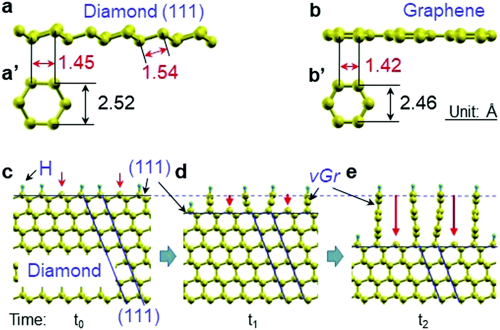 | ||
| Fig. 3 Schematic diagrams showing the diamond (111) plane with graphene and the formation mechanism of the vGr-diamond hybrid structures. (a and b) Atomic models showing structural similarity between (zigzag) diamond (111) and (flat) graphene. (a′ and b′) Top views of diamond (111) and graphene, respectively. Both reveal a hexagonal structure. (c–e) Schematic diagrams depicting the formation mechanism of the vGr-diamond hybrid structures on a diamond (111) surface. Each dangling carbon atom is attached with a hydrogen atom before starting (t0) the transformation of the diamond (111) plane to graphene layers (c). The red arrows in (c) indicate the site where atomic hydrogen is detached, whereas the solid red arrows in (b and c) indicate the inward etching of the graphene layers. The time indicates the duration of the plasma treatment (t1 < t2.). | ||
The normal scan of the XRD pattern reveals the strongest 〈110〉 peak, demonstrating that the diamond plate is 〈110〉 textured (inset in Fig. 4a) where the surface is covered with (110) planes. The low angle X-ray pattern measured for the hybrid structure reveals a peak at 2θ = 22.8°, together with (111) and (220) peaks of diamond. The unique peak represents an average spacing of graphene layers, ∼3.90 Å, which is larger by 11–16% than those of conventional graphite, 3.35 Å, 3.44 Å and 3.53 Å for AB, AA′ and AA stacking,19 and thus, this becomes evidence for their epitaxial growth onto the diamond plate. Indeed, the spacing is similar to ∼3.75 Å, which is expected at the free end of graphene layers (Fig. 1a). The rocking curve XRD shown in Fig. 4b demonstrates that the graphene layers were inclined by 60° to the perpendicular direction of the diamond plate (30° to the diamond (110) surface) (inset in Fig. 4b). These provide ‘XRD evidence’ for the epitaxial growth of graphene onto 〈110〉 textured diamond, supporting the transformation mechanism of diamond (111) to graphene on 〈110〉 textured diamond films (Fig. S3, ESI†).
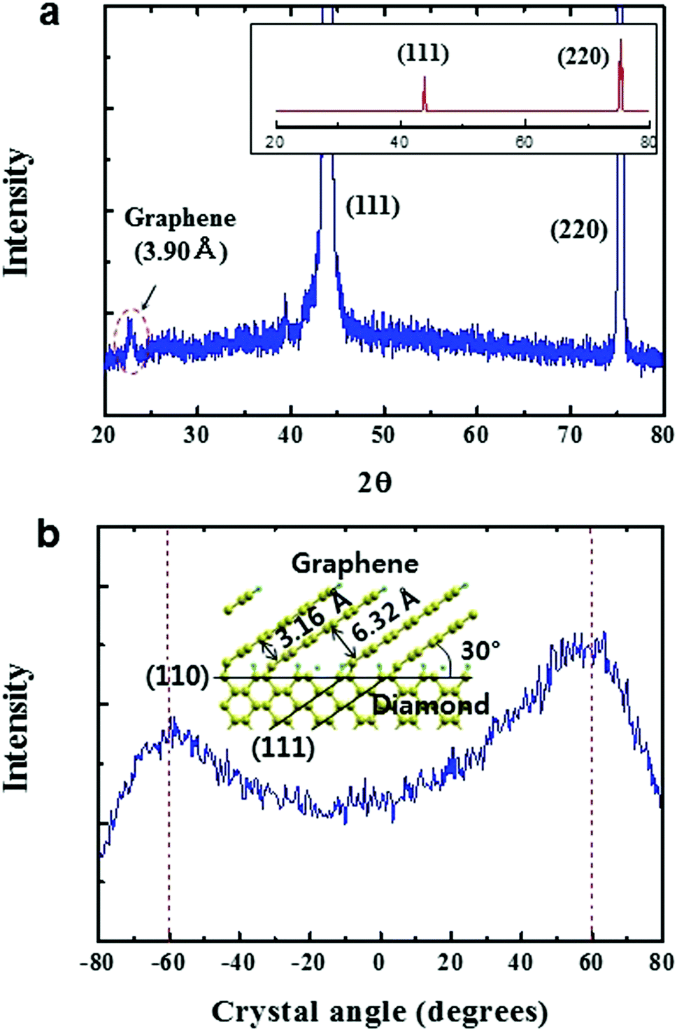 | ||
| Fig. 4 The XRD analysis for the hybrid structure. (a) Low angle XRD pattern. The inset shows a normal scan XRD pattern indicating that the diamond plate is 〈110〉 textured. (b) Rocking curve XRD data for the 3.90 Å peak for graphene shown in (a). The inset shows an atomic model showing the epitaxial growth of graphene layers on a (110) plane of diamond (Fig. S3, ESI†). | ||
However, the localized SEM pattern (Fig. 2b) can be explained by transformation of the different (111) planes (Fig. S4, ESI†) to graphene layers (Fig. 3) although it can also be due to grain (twin) boundaries of the 〈110〉 textured diamond film. The analysis indicates that the unique SEM pattern becomes ‘morphological evidence’ for the epitaxial growth of graphene layers.
With the hybridization, dramatic changes are observed in PL spectra, as shown in Fig. 5a. A prominent band with a peak at ∼2.78 eV (∼450 nm) evolves whereas the band at ∼2.00 eV (∼600 nm) disappears. This is attributed to the strong peak revealed at 2.78 eV which is the interface defects of the vGr-diamond hybrid structure (Fig. 1a and b). The disappearance of the strong band at ∼2.00 eV was attributed to the quenching of the defects in the diamond with the heating at 1300 °C under hydrogen plasma. The band at ∼1.88–2.02 eV is due to nitrogen related defects (NV0),29–31 whereas a small broad band at 2.47 eV (Fig. 5a) is due to nitrogen related defects [H3 (2.46 eV) and H4 (2.49 eV)] or carbon related defects [3H (2.43 eV)].31–33
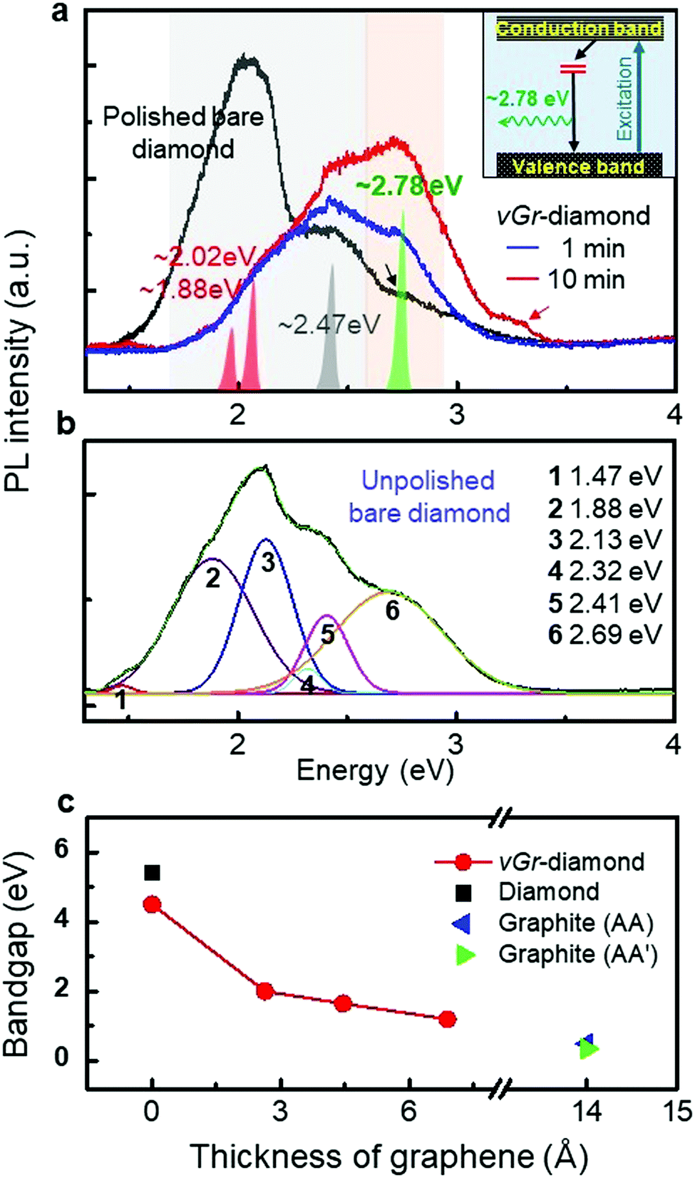 | ||
| Fig. 5 The PL and simulation data for bare diamond and vGr-diamond hybrid structures. (a) PL data. The shaded peaks are assigned via the deconvolution of the spectra (Fig. S5, ESI†). The inset shows an energy band diagram. It is thought that the signal at ∼3.25 eV (red arrow) may be due to a defect reformed during the etching process. (b) The PL spectrum for an unpolished bare diamond, deconvoluted into six peaks, including the 2.69 eV peak. (c) The band gap landscape of diamond-graphene hybrid structures compared with their constituents (diamond and AA and AA′ graphite). | ||
Kupriyanov et al. observed a sharp zero phonon line (ZPL) at 2.75 eV (∼450 nm) with replicas, which appeared on a PL spectrum measured from heat-treated (2500 °C) HPHT diamond at 77 K.34 They assigned the 2.75 eV peak to ZPL. Martineau et al. summarized the common features observed in the spectra of some as-grown and HPHT-treated CVD diamond as a table where the PL signals such as the 425 nm (∼2.92 eV), and 451–459 nm (2.75–2.70 eV) series of lines, and 503 nm (2.47 eV) (observable from our hybrid samples: Fig. 5a) are listed,35 citing Zaitsev's book.36 It was expected that the surfaces of the HPHT-treated diamond samples might be modified in a similar way to ones described here due to the high temperatures.
However, bare diamond reveals a weak signal at ∼2.78 eV (arrow in Fig. 5a). The PL spectrum for an ‘unpolished’ bare diamond plate reveals a unique peak at ∼2.69 eV together with peaks at 2.41, 2.32, 2.13, 1.88, and 1.47 eV (Fig. 5b). The peak weakens with polishing (Fig. S6, ESI†), indicating that its intensity depends on the relative surface area of the polycrystalline diamond. The 2.69 eV peak was assigned to ‘surface defects’ (including grain boundaries) of the CVD diamond. The analysis indicates a blue shift of the interface defects by ∼90 meV, due to the compressive strain of the C2 atoms in the interface of the hybrid structures. The shift is consistent with what happens with MoS2 and WS2,37 and corresponds to ∼3% strain based on the data of 23.9 and 36.3 meV %−1 for MoS2 and WS2, respectively.
It is generally understood that strain in graphene changes the band gap.17 The calculated band gap (∼1.00 eV) of the hybrid structure (Fig. 1c) was attributed to the C1 atom (Fig. 1b), launching the parallel graphene layers with a 1:1 registry, thus under a strain due to their narrower spacing of 2.19 Å. The strain causes electronic transitions in their 2px + 2py orbitals, resulting in band gap opening at 1.20 eV (Fig. 1d), which approaches ∼1.00 eV for the hybrid structure. Further simulations show evolution of the band gap as a function of the graphene thickness grown on the diamond surfaces (Fig. 5c). The band gap decreases from ∼1.85 eV to ∼0.25 eV (due to relaxation of strain) with increasing thickness of graphene up to ∼1.4 nm on the diamond surface, showing the way for future band gap engineering of diamond.
However, the thickness of the graphene layers (5-50 nm) of vGr-diamond (Fig. S2, ESI†) is out of the range for band gap engineering. It was not easy to control the exact thickness of graphene ∼1.4 nm via plasma etching due to the high temperature of 1300 °C (measured by a pyrometer). The graphene face of a vGr-diamond hybrid structure (with graphene layers of ∼50 nm thickness) was scrubbed on sandpaper (#1200) to shorten the graphene layers. The scrubbed face goes back to the mirror surface of the polished diamond whereas its Raman D and G peaks nearly disappear (leaving their traces) without changing the PL signal, as shown in Fig. 6. The RMS of the scrubbed face was ∼9 nm (Fig. S7, ESI†), which was three times higher than that of mirror polished bare diamond (∼3 nm) due to the graphene layers torn out by the scrubbing. The data indicate that further polishing (mechanical or chemical polishing, and plasma etching) the graphene face after hybridization can be a supplementary way of controlling the graphene layers to the effective thickness of ∼1.4 nm (Fig. 5c). Vertical graphene, thicker than a few nm, hybridized onto diamond may also reveal a band gap, corresponding to the intrinsic band gap of AA (0.50 eV) and AA′ (0.35 eV) stacked graphene planes.38,39
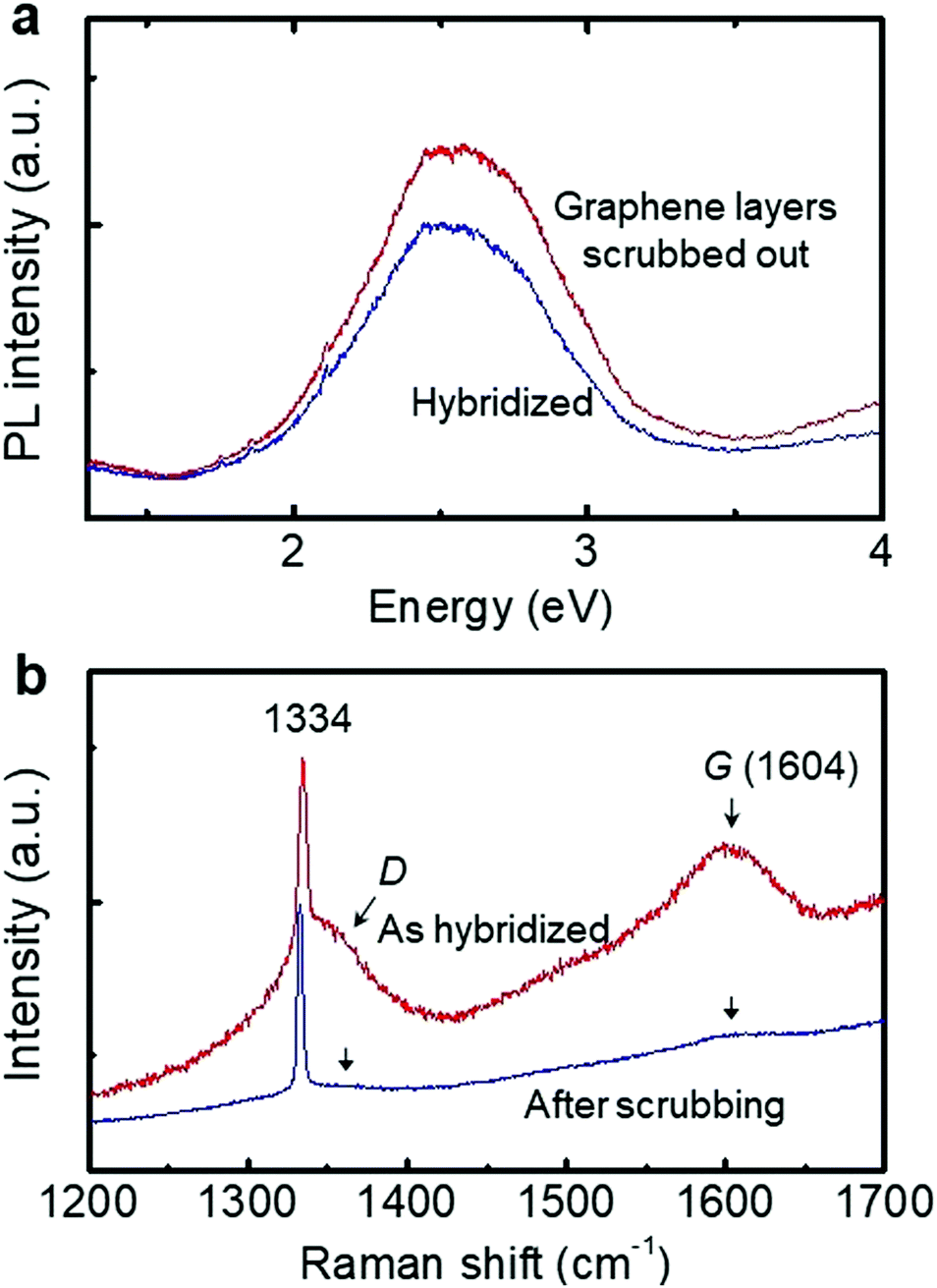 | ||
| Fig. 6 The PL and Raman spectra measured from the graphene side of a vGr-diamond hybrid structure, before (as hybridized) and after scrubbing. (a) PL spectra. (b) Raman spectra. Arrows on the Raman spectrum of the graphene side (scrubbed) indicate traces of D (∼1360 cm−1) and G (∼1604 cm−1). | ||
In summary, an electronic transition at ∼2.78 eV was demonstrated by CVD diamond based graphene hybrid structures, which was supported by unique and consistent morphological, XRD and Raman evidence. The electronic transition was assigned to the interface defects of the hybrid structure, comparable with the peak at 2.69 eV from the surface defects of a CVD diamond. Simulations indicated that the C1 interface atom under a strain and the thickness of the graphene layers may control the band gap of the diamond. This study, demonstrating the functionalization of diamond, may provide a clue to engineering the band structure of diamond free from the degradation of the crystallinity.
Conflicts of interest
There are no conflicts to declare.Acknowledgements
The work was supported by the KIST Future Resource Program (2E29420). The simulations were carried out using the Server farm supercomputing facility at KIST. The Raman and PL analyses were performed with equipment in the Gwangju Center of the Korea Basic Science Institute.Notes and references
- M. Kamo, Y. Sato, S. Matsumoto and N. Setaka, Diamond synthesis from gas phase in microwave plasma, J. Cryst. Growth, 1983, 62, 642 CrossRef CAS.
- J. E. Butler and R. L. Woodin, Thin film diamond growth mechanisms, Philos. Trans. R. Soc., A, 1993, 342, 209 CrossRef CAS.
- H. Kawarada, M. Aoki and M. Ito, Enhancement mode metal-semiconductor field effect transistors using homoepitaxial diamonds, Appl. Phys. Lett., 1994, 65, 1563 CrossRef CAS.
- C. J. H. Wort and R. S. Balmer, Diamond as an electronic material, Mater. Today, 2008, 11, 22 CrossRef CAS.
- C.-S. Yan, Y. K. Vohra, H.-K. Mao and R. J. Hemley, Very high growth rate chemical vapor deposition of single-crystal diamond, Proc. Natl. Acad. Sci. U. S. A., 2002, 99, 12523 CrossRef CAS.
- J.-H. Seo, H. Wu, S. Mikael, H. Mi, J. P. Blanchard, G. Venkataramanan, W. Zhou, S. Gong, D. Morgan and Z. Ma, Thermal diffusion boron doping of single-crystal natural diamond, J. Appl. Phys., 2016, 119, 205703 CrossRef.
- S. Koizumi, C. Nebel and M. Nesladek, Physics and Applications of CVD Diamond, Wiley-VCH Verlag GmbH & Co. KgaA, 2008 Search PubMed.
- R. Kalish, C. Uzan-Saguy, A. Samoiloff, R. Lecher and P. Koidl, Doping of polycrystalline diamond by boron ion implantation, Appl. Phys. Lett., 1994, 64, 2532 CrossRef CAS.
- J. F. Prins, Activation of boron-dopant atoms in ion-implanted diamonds, Phys. Rev. B: Condens. Matter Mater. Phys., 1988, 38, 5576 CrossRef CAS.
- C.-K. Chang, S. Kataria, C.-C. Kuo, A. Ganguly, B.-Y. Wang, J.-Y. Hwang, K.-J. Huang, W.-H. Yang, S.-B. Wang, C.-H. Chuang, M. Chen, C.-I. Huang, W.-F. Pong, K.-J. Song, S.-J. Chang, J.-H. Guo, Y. Tai, M. Tsujimoto, S. Isoda, C.-W. Chen, L.-C. Chen and K.-H. Chen, Band Gap Engineering of Chemical Vapor Deposited Graphene by in Situ BN Doping, ACS Nano, 2013, 7, 1333 CrossRef CAS.
- Z. Liu, L. Ma, G. Shi, W. Zhou, Y. Gong, S. Lei, X. Yang, J. Zhang, J. Yu, K. P. Hackenberg, A. Babakhani, J.-C. Idrobo, R. Vajtai, J. Lou and P. M. Ajayan, In-plane heterostructures of graphene and hexagonal boron nitride with controlled domain sizes, Nat. Nanotechnol., 2013, 8, 119 CrossRef CAS.
- W. Yang, G. Chen, Z. Shi, C.-C. Liu, L. Zhang, G. Xie, M. Cheng, D. Wang, R. Yang, D. Shi, K. Watanabe, T. Taniguchi, Y. Yao, Y. Zhang and G. Zhang, Epitaxial growth of single-domain graphene on hexagonal boron nitride, Nat. Mater., 2013, 12, 792 CrossRef CAS.
- X. Liu and Z. Li, Electric Field and Strain Effect on Graphene-MoS2 Hybrid Structure: Ab Initio Calculations, J. Phys. Chem. Lett., 2015, 6, 3269 CrossRef CAS.
- J. Xue, J. Sanchez-Yamagishi, D. Bulmash, P. Jacquod, A. Deshpande, K. Watanabe, T. Taniguchi, P. Jarillo-Herrero and B. J. LeRoy, Scanning tunnelling microscopy and spectroscopy of ultra-flat graphene on hexagonal boron nitride, Nat. Mater., 2011, 10, 282 CrossRef CAS.
- M. Yankowitz, J. Xue, D. Cormode, J. D. Sanchez-Yamagishi, K. Watanabe, T. Taniguchi, P. Jarillo-Herrero, P. Jacquod and B. J. LeRoy, Emergence of superlattice Dirac points in graphene on hexagonal boron nitride, Nat. Phys., 2012, 8, 382 Search PubMed.
- N. Huo, Z. Wei, X. Meng, J. Kang, F. Wu, S.-S. Li, S.-H. Wei and J. Li, Interlayer coupling and optoelectronic properties of ultrathin two-dimensional heterostructures based on graphene, MoS2 and WS2, J. Mater. Chem. C, 2015, 3, 5467 RSC.
- J. Wang, F. Ma and M. Sun, Graphene, hexagonal boron nitride, and their heterostructure: properties and applications, RSC Adv., 2017, 7, 16801 RSC.
- W. R. L. Lambrecht, C. H. Lee, B. Segall, J. C. Angust, Z. Lit and M. Sunkara, Diamond nucleation by hydrogenation of the edges of graphitic precursors, Nature, 1993, 364, 607 CrossRef CAS.
- J.-K. Lee, S.-C. Lee, J.-P. Ahn, S.-C. Kim, J. I. B. Wilson and P. John, The growth of AA graphite on (111) diamond, J. Chem. Phys., 2008, 129, 234709 CrossRef.
- S. Tulic, T. Waitz, M. Caplovicova, G. Habler, M. Varga, M. Kotlar, V. Vretenar, O. Romanyuk, A. Kromka, B. Rezek and V. Skakalova, Covalent Diamond-Graphite Bonding: Mechanism of Catalytic Transformation, ACS Nano, 2019, 13, 4621 CrossRef CAS PubMed.
- J.-K. Lee, K. Y. Eun, Y.-J. Baik, H. J. Cheon, J. W. Rhyu, T. J. Shin and J.-W. Park, The large area deposition of diamond by the multi-cathode direct current plasma assisted chemical vapor deposition (DC PACVD) method, Diamond Relat. Mater., 2002, 11, 463 CrossRef CAS.
- J. Hodkiewicz, Characterizing Carbon Materials with Raman Spectroscopy, Thermo Fisher Scientific, 2010 Search PubMed.
- M. Hanfland, H. Beister and K. Syassen, Graphite under pressure: Equation of state and first-order Raman modes, Phys. Rev. B: Condens. Matter Mater. Phys., 1989, 39, 12598 CrossRef CAS.
- D. S. Knight and W. B. White, Characterization of diamond films by Raman spectroscopy, J. Mater. Res., 1989, 4, 385 CrossRef CAS.
- M. Nagai, K. Nakanishi, H. Takahashi, H. Kato, T. Makino, S. Yamasaki, T. Matsumoto, T. Inokuma and N. Tokuda, Anisotropic diamond etching through thermochemical reaction between Ni and diamond in high-temperature water vapour, Sci. Rep., 2018, 8, 6687 CrossRef.
- J.-M. Zhang, F. Ma, K.-W. Xu and X.-T. Xin, Anisotropy analysis of the surface energy of diamond cubic crystals, Surf. Interface Anal., 2003, 35, 805 CrossRef CAS.
- M. Seal, Graphitization and Plastic Deformation of Diamond, Nature, 1958, 182, 1264 CrossRef CAS.
- R. A. Khmelnitsky and A. A. Gippius, Transformation of diamond to graphite under heat treatment at low pressure, Phase Transitions, 2014, 87, 175 CrossRef CAS.
- F. Treussarta, V. Jacquesa, E. Wua, T. Gacoinb, P. Grangierc and J.-F. Rocha, Photoluminescence of single colour defects in 50 nm diamond nanocrystals, Phys. B, 2006, 376–377, 926 CrossRef.
- M. C. Rossi, S. Salvatori, F. Galluzzi, F. Somma and R. M. Montereali, Diamond photoluminescence spectra: dependence on excitation energy and microstructure, Diamond Relat. Mater., 1998, 7, 255 CrossRef CAS.
- H.-C. Lu, M.-Y. Lin, S.-L. Chou, Y.-C. Peng, J.-I. Lo and B.-M. Cheng, Identification of Nitrogen Defects in Diamond with Photoluminescence Excited in the 160–240 nm Region, Anal. Chem., 2012, 84, 9596 CrossRef CAS PubMed.
- J. Walker, Optical absorption and luminescence in diamond, Rep. Prog. Phys., 1979, 42, 1605 CrossRef CAS.
- I. Nasieka, V. Strelchuk, M. Boyko, V. Voevodin, A. Vierovkin, A. Rybka, V. Kutniy, S. Dudnik, V. Gritsina, O. Opalev and V. Strel’nitskij, Raman and photoluminescence characterization of diamond films for radiation detectors, Sens. Actuators, A, 2015, 223, 18 CrossRef CAS.
- I. N. Kupriyanov, V. A. Gusev, Y. M. Borzdov, A. A. Kalinin and Y. N. Palyanov, Photoluminescence study of annealed nickel- and nitrogen-containing synthetic diamond, Diamond Relat. Mater., 1999, 8, 1301 CrossRef CAS.
- P. M. Martineau, S. C. Lawson, A. J. Taylor, S. J. Quinn, D. J. F. Evans and M. J. Crowder, Identification of synthetic diamond grown using chemical vapor deposition, Gems Gemol., 2004, 40, 2 CrossRef CAS.
- A. M. Zaitsev, Optical Properties of Diamond, Springer-Verlag, Berlin, 2001, p. 502 Search PubMed.
- S. Park, J. Lee, Y.-W. Lee, A. Jang, S. Ahn, K. Y. Ma, Y. Cho, J. Hong, S. Lee, H. Y. Jeong, H. Im, H. S. Shin, S. M. Morris, S. Cha, J. I. Sohn and J. M. Kim, Strain-mediated interlayer coupling effects on the excitonic behaviors in an epitaxially grown MoS2/WS2 van der Waals, Nano Lett., 2017, 17, 5634 CrossRef.
- J.-K. Lee, J.-G. Kim, K. P. S. S. Hembram, Y.-I. Kim, B.-K. Min, Y. Park, J.-K. Lee, D. J. Moon, W. Lee, S.-G. Lee and P. John, Nature of Metastable AA′ Graphite: Low Dimensional Nano- and Single-Crystalline Forms, Sci. Rep., 2016, 6, 39624 CrossRef CAS.
- E. J. Mele, Commensuration and interlayer coherence in twisted bilayer graphene, Phys. Rev. B: Condens. Matter Mater. Phys., 2010, 81, 161405 CrossRef.
Footnotes |
| † Electronic supplementary information (ESI) available. See DOI: 10.1039/c9mh01588d |
| ‡ These authors contributed equally to this work. |
| This journal is © The Royal Society of Chemistry 2020 |