
 Open Access Article
 This Open Access Article is licensed under a
 Creative Commons Attribution 3.0 Unported Licence
Interface limited hole extraction from methylammonium lead iodide films†
Oskar
Blaszczyk
 ,
Lethy
Krishnan Jagadamma
,
Arvydas
Ruseckas
,
Muhammad T.
Sajjad
,
Yiwei
Zhang
and
Ifor D. W.
Samuel
*
,
Lethy
Krishnan Jagadamma
,
Arvydas
Ruseckas
,
Muhammad T.
Sajjad
,
Yiwei
Zhang
and
Ifor D. W.
Samuel
*
Organic Semiconductor Centre, SUPA, School of Physics and Astronomy, University of St Andrews, St Andrews, Fife KY16 9SS, UK. E-mail: ar30@st-andrews.ac.uk; idws@st-andrews.ac.uk
First published on 9th December 2019
Abstract
Small solar cells based on metal halide perovskites have shown a tremendous increase in efficiency in recent years. These huge strides in device performance make it important to understand processes such as accumulation and extraction of charge carriers to better address the scalability and stability challenges which have not been solved yet. In most studies to date it is unclear whether the limiting factor of charge extraction is charge transport in the bulk of the perovskite or transfer across the interface with the charge extracting layer, owing largely to the inaccessibility of buried interfaces. Separating bulk and interfacial effects on charge extraction can help the search for new charge extracting materials, improve understanding of charge transport in active layer materials and help optimise device performance; not only in the laboratory setting but also for commercial production. Here we present a method to unambiguously distinguish between bulk and interface effects on charge extraction dynamics which is based on time-resolved photoluminescence with different excitation density profiles. We use this method to study charge extraction from solution-deposited CH3NH3PbI3 films to NiO and PEDOT:PSS layers. We find that NiO shows faster hole extraction than PEDOT:PSS from the 300 nm thick perovskite film on the time scale of 300 ps which is independent of charge carrier density in the region of 1016–1017 cm−3. The interface with NiO is found to only slightly limit charge extraction rate at charge densities exceeding 1016 cm−3 as the extraction rate is fast and does not decrease with time. This is in contrast to PEDOT:PSS where we find the charge extraction rate to be slower, decreasing with time and dependent on charge density in the region 1016–1017 cm−3 which we interpret as charge accumulation at the interface. Hence we find that charge extraction is severely limited by the interface with PEDOT:PSS. These findings are confirmed by transient absorption spectroscopy. A hole diffusion coefficient of D = (2.2 ± 0.5) cm2 s−1 was determined in the perovskite film that is independent of charge density. This indicates a band-like hole transport regime, not observed for solution processed films before. Our findings stress the importance of interface optimization in devices based on perovskite active layers as there is still room for improvement of the hole extraction rate even in the case of the superior NiO layer.
New conceptsSolution processable hybrid perovskites have emerged in the last few years as very attractive materials for optoelectronic applications, especially in photovoltaics. Free carriers generated in the active layer of solar cells must be quickly extracted to the electrodes to avoid recombination losses. Carrier extraction includes transport in the active layer and transfer across the interface towards electrodes. To date it has been very difficult to determine which one of these processes limits charge extraction and to separate their effects experimentally. Here we present a method for unambiguously separating bulk and interface effects on charge extraction and use it to show that hole transfer from a hybrid perovskite film to the widely used hole extraction layer of PEDOT:PSS limits the overall extraction rate at standard solar cell working conditions. A thin layer of NiO is found to facilitate fast hole extraction even at high charge densities which occur in solar cells used with light concentrators. Our results show the importance of interface optimization to improve charge extraction in perovskite solar cells and provide a window into the role of buried interfaces not available before. |
Introduction
Perovskites have had tremendous success in recent years as materials for optoelectronic applications. Performance of perovskite solar cells (PSC) has been improving very fast and has reached efficiencies exceeding 25%. Low exciton binding energy,1 strong absorption2 and superior charge transport properties3 combined with low cost fabrication from solution is making them attractive solar cell materials. However, the problems of scaling-up, short operational lifetimes and choice of transport layer materials are still not resolved. To solve them it is crucial to understand the factors limiting charge extraction which includes transport in the charge generation and extraction layers as well as at their interfaces. Many attempts at measuring and enhancing charge transport in the most popular perovskite, CH3NH3PbI3 (MAPbI3 or MAPI) have been published in the literature.3–6 The reported values of the charge diffusion coefficient in solution processed MAPbI3 films range from ∼10−5 to 2.7 cm2 s−1 spanning five orders of magnitude.6 This can be partly explained by different material properties of the same stoichiometry perovskites depending on the synthesis, deposition method, post processing and substrate choice, but in addition different measurement techniques and experiment conditions can give different results. Transient grating technique has revealed weak dependence of the ambipolar carrier diffusion coefficient on carrier density in perovskites of high compositional quality whilst other films showed very strong dependence on carrier density which was attributed to trap filling.7 Another recent study has shown indications of different lattice reorganizations around excitons and charges in hybrid perovskites which are very likely to affect exciton and charge localization and transport.8 Here we show carrier density independent hole transport in solution processed MAPbI3 perovskite films which so far has only been observed in vapor deposited films at high excitation densities in the range of 1018–1019 cm−3.7 Furthermore, we demonstrate this trap-free transport at low excitation densities, more relevant to solar cell operation.The preparation of charge extraction layers is also crucial to the operation of the PSC as the transfer across the interface with the active layer is the second factor determining charge extraction from the solar cell. In traditional n–i–p solar cell geometry, where the top transparent contact is the anode and the bottom electrode is the cathode, Spiro-OMeTAD and PTAA are commonly used as hole extraction layer (HEL) materials, adjacent to the anode. This structure leads to one of the highest power conversion efficiencies reported9 but problems with charge transporting materials, such as the high temperature needed to fabricate the mesoporous TiO2, complex doping and high cost of the commonly used HELs10 are making researchers look towards both different device architectures and HELs. One interesting proposition is to use the “inverted” p–i–n architecture, where the top contact is the transparent cathode, the bottom contact is the anode and the perovskite is deposited on the HEL. To date this has been attempted mainly with PEDOT:PSS as the HEL. The simplicity of fabrication, low processing temperature and compatibility with roll-to-roll manufacturing processes make this an attractive solar cell architecture but it suffers problems with efficiency and stability, partly due to its acidity, temperature sensitivity and hygroscopic properties.10 A low processing temperature and stable hole transporting layer based on NiO nanoparticles has been proposed as a superior HEL recently by Jagadamma et al.11 but it is still unclear what the underlying reasons for improved charge extraction from the solar cell are and what role charge transport and interfacial transfer rate play in charge extraction, making it very difficult to compare between different charge extracting materials even for the same perovskite composition and preparation method. This information is crucial when aiming to develop solar cells with hot carrier extraction which potentially can break the Shockley–Queisser limit.12
Surface quenching of time resolved photoluminescence (PL) has been previously employed to measure the charge carrier diffusion coefficient in perovskites3,4 as well as the exciton diffusion coefficient in organic semiconductors.13 In this technique it is common to assume that quenching is transport limited and quenching occurs on the first passage to the interface (perfect quencher condition). However, if excitons or charges can escape quenching by diffusing away, then the perfect quencher assumption underestimates the diffusion coefficient. It is difficult to access information directly about the processes at embedded interfaces on the time scales relevant to charge extraction using surface spectroscopy techniques. Here we demonstrate that by creating photogenerated charge carrier populations at opposite ends of the studied films we can simultaneously determine the value of the diffusion coefficient and interfacial quenching rate. We show that hole extraction from MAPbI3 perovskite to Nickel Oxide (NiO) layer occurs on a timescale of about 300 ps, which is about twice longer than the value predicted by the perfect quencher model. In the case of PEDOT:PSS hole transfer across the interface limits the overall extraction rate severely, especially at higher charge densities, and slows down as time progresses. This indicates hole accumulation at the interface with PEDOT:PSS which can be explained by low hole mobility in this extraction layer and can lead to detrimental effects on device performance.14
Experimental
The solution to make the perovskite active layer was prepared by mixing 461 mg of PbI2 (Alfa Aesar 99.999%) and 159 mg of CH3NH3I (Dyesol) in a mixed solvent of dimethyl sulfoxide (66 μL) (DMSO, Sigma Aldrich, anhydrous, 99.9%) and dimethyl-formamide (636 μL) (DMF, Sigma Aldrich, anhydrous, 99.9%). The precursor solution was stirred for 1 hour at room temperature and then spin-coated onto the glass/ITO/NiO substrates at 4000 rpm for 30 seconds. During the first 7 s of the spin-coating process, a diethyl ether wash (700 μL) was carried out. After completing the spin coating process, the perovskite film was annealed in reduced pressure of nitrogen (∼100 mbar) at 100 °C for 1 minute followed by annealing in nitrogen in the glovebox for another 2 minutes. Film thickness was measured by a Dektak profilometer to be 300 nm.NiO nanoparticle thin films were prepared from the NiO nanoparticle suspension (Avantama, P-21, product number 10128, 7 nm particle size) from Avantama. The as-received NiO nanoparticles were ultra-sonicated for 1 minute followed by diluting (1![[thin space (1/6-em)]](https://www.rsc.org/images/entities/char_2009.gif) :10 by volume) the suspension in anhydrous ethanol. The diluted NiO nanoparticle suspension was sonicated for 5–10 minutes before spin coating. The spin coating was carried out under ambient conditions, at 2000 rpm for 60 seconds. After spin coating, the glass/ITO/NiO substrates were annealed at 100 °C for 10 minutes.
:10 by volume) the suspension in anhydrous ethanol. The diluted NiO nanoparticle suspension was sonicated for 5–10 minutes before spin coating. The spin coating was carried out under ambient conditions, at 2000 rpm for 60 seconds. After spin coating, the glass/ITO/NiO substrates were annealed at 100 °C for 10 minutes.
The absorbance spectra of the films were measured using a Varian Cary 300 UV-Vis Spectrophotometer. Time resolved photoluminescence was measured using a Hamamatsu C6860 synchroscan streak camera. The films were excited using 200 fs pulses at 640 nm with a 200 kHz repetition rate. For surface quenching, measurements from two sides of the samples were taken, the perovskite side and the substrate side.
Transient absorption spectroscopy was carried out using HARPIA spectrometer from Light Conversion. The films were excited using 640 nm pump pulses of 200 fs duration at 50 kHz repetition rate from a PHAROS regenerative amplifier (Light Conversion). The white light continuum used as the probe was generated using a sapphire plate and its total energy was kept below 1% of the pump pulse energy.
Results and discussion
To optically characterize the solution processed thin films of MAPbI3/glass, MAPbI3/NiO and, MAPbI3/PEDOT:PSS we used UV-vis absorption, time resolved photoluminescence and transient absorption spectroscopies. Fig. 1 shows the UV-Vis and time integrated PL spectra along with a TA spectrum at 2 ps after excitation.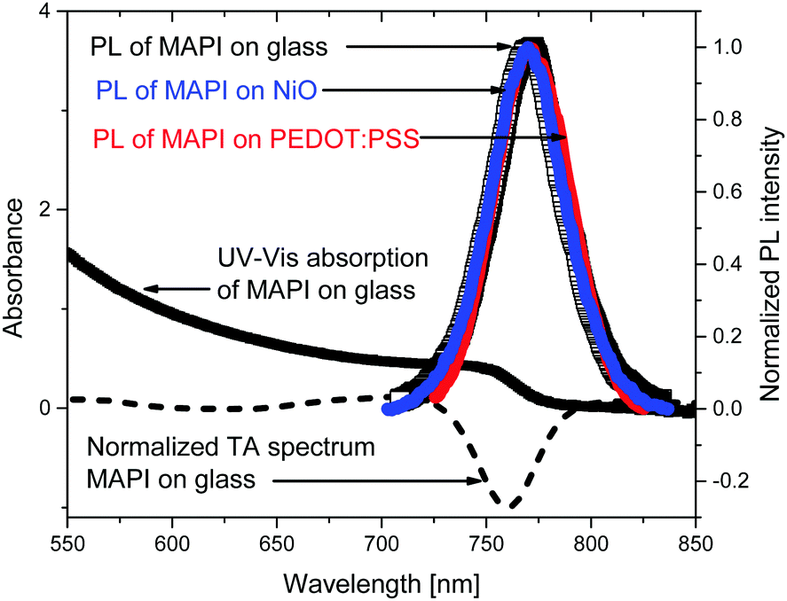 | ||
| Fig. 1 UV-Vis absorption spectrum of a bare MAPbI3 film on glass and normalized photoluminescence spectra (PL) of the perovskite on glass (black empty squares), perovskite quenched by PEDOT:PSS (red line) and perovskite quenched by NiO (blue line) integrated in the time window from 0 to 1.6 ns after excitation at 640 nm. Transient absorption (TA) spectrum at 2 ps after excitation at 640 nm is shown by a dashed line. | ||
The films show strong absorption with the absorption edge half height at 765 nm. The shape is characteristic of band-to-band absorption with no pronounced exciton peak visible at the band edge. The absorbance increases with the photon energy resulting in short absorption lengths compared with sample thickness (300 nm) in the whole of the visible light region. The absence of additional peaks also suggests the dominance of a single crystalline phase which is further supported by a narrow PL spectrum which shows a single peak at 772 nm. The photoluminescence spectra of the MAPbI3 film deposited on NiO and on PEDOT:PSS and integrated from 0 to 1.6 ns after excitation show the same spectral shape as a bare MAPbI3. This indicates that morphology and composition of the bare MAPbI3 film and on NiO and on PEDOT:PSS is very similar. This is further supported by very similar transient absorption (TA) spectra of bare MAPbI3 film and on NiO and on PEDOT:PSS. TA spectra are dominated by the ground state bleach at the band edge where the onset of steady state absorption is observed and show no spectral evolution from 1 ps to 2 ns (Fig. S1, ESI†). The narrow spectral shape of TA spectra and absence of spectral dynamics on a picosecond time scale suggest very few trap states present in the bulk of the perovskite, further supported by the narrow shape of the PL.
To investigate the morphology of the perovskite layer deposited on top of the different substrates further, we performed scanning electron microscopy (Fig. S2, ESI†). The perovskite grown on top of both substrates forms a dense film with no visible pinholes. The domain sizes for both cases are similar and range between 100–350 nm. Some aggregate features are seen on the grain boundaries in both films. It was therefore concluded that the perovskite morphology is similar for films grown on top of PEDOT:PSS and NiO. To check the crystallinity, we performed X-ray diffraction measurement (Fig. S3, ESI†). We observed that the perovskite films deposited on top of the different substrates had the same intensity of diffraction peaks. We therefore concluded that the crystallinity of the different samples was similar.
To determine the hole diffusion coefficient of MAPbI3 we performed a variation on the photoluminescence surface quenching experiment, a well-established method for organic semiconductors,13 that has been previously applied to perovskites.3,4 In this experiment the perovskite active layer is in contact with a layer of quenching material in a bilayer geometry as shown in Fig. 2. Following a pulsed laser excitation, the time-resolved photoluminescence intensities from the perovskite films with the quenching layer and without it carry information about charge extraction dynamics. The absorption profile is calculated using Beer–Lambert law and over 90% of the incident laser pulse intensity is absorbed in the perovskite active layer. A model, based on the diffusion equation (eqn (1)), is then used to simulate the dynamics of charge carriers within the material and the resulting simulated PL decay is fitted to the experimental data by adjusting the value of the fitting parameter, most commonly the diffusion coefficient.
 | (1) |
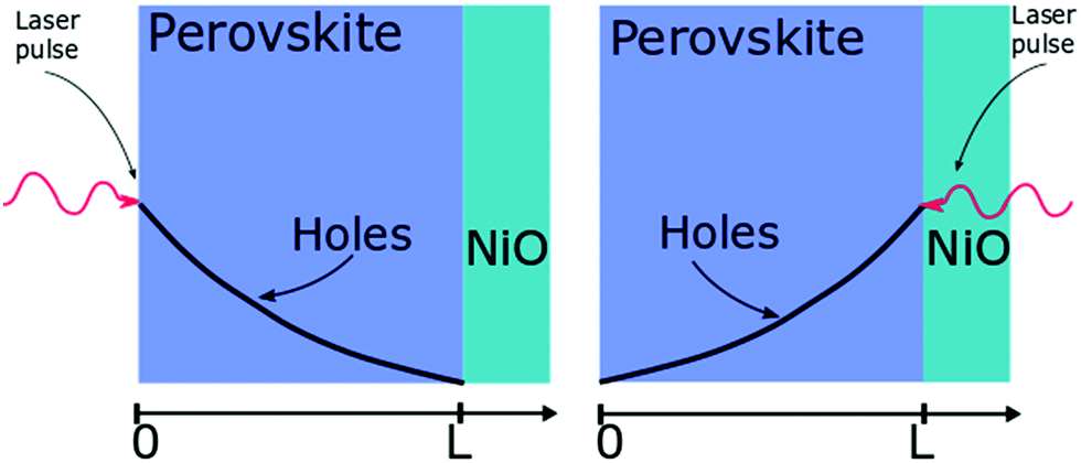 | ||
| Fig. 2 Layout of the surface quenching experiment with perovskite side illumination (left hand side) and substrate side illumination (right hand side) and the initial hole density profiles at t = 0. | ||
The initial distribution of charge carriers as well as their behavior at interfaces is determined by the choice of the initial and boundary conditions in the model. In most surface quenching experiments to date, the choice of the boundary conditions at the quenching interface has been such as to assume perfect quenching at one interface and perfect reflection from the other interface, hence, p(x = L,t) = 0 and ∂p(x = 0,t)/∂x = 0. As long as the charge carrier diffuses to the interface it is quenched immediately and with 100% efficiency. In the case of slow diffusion in organic semiconductors with relatively fast interfacial quenching, it has been shown this is a good approximation.13 However, it is unclear if this can be applied to hybrid perovskites with high charge carrier diffusivity and if imperfect quenching boundary condition should be used instead as discussed in previous work by other researchers on organic semiconductors15 and quantum dots.16 A finite rate of quenching should be applied instead which can be represented by the boundary condition D∂p(x = L,t)/∂x = −k × p(x,t), where the quenching rate at the interface is equated to the diffusive flux of species across the interface. Further details about the solution to the diffusion equation and the parameters used are provided in ESI.†
Here we demonstrate that performing the conventional surface quenching experiment for hybrid perovskites with high charge diffusion coefficients is not an appropriate method for determining the diffusion coefficient as it leads to a severe under-estimation of its value unless the interface is a perfect quencher. We further notice that this is only apparent when applying the diffusion model to two distinct cases as seen in Fig. 2. In the first case, when the laser light is incident on the film from the perovskite layer side, a distribution of photogenerated charge carriers is created that has a maximum far from the interface. This way the charged species can diffuse towards the interface giving us information about the diffusion process [Fig. 2]. When the laser light is incident from the substrate side [Fig. 2] a high concentration of charged species is created directly next to the interface with the quencher, providing us with more information about the quenching process at the interface as diffusion becomes less important. We note that this allows us to determine if charge extraction is diffusion or interface limited as well as to determine the value of the diffusion coefficient and the quenching rate simultaneously.
The time resolved PL data for the bare perovskite on glass, MAPbI3/NiO and MAPbI3/PEDOT:PSS films are presented in Fig. 3 and clearly show a much faster decay of the MAPbI3/NiO film compared with both MAPbI3/glass and MAPbI3/PEDOT:PSS films indicating that NiO facilitates faster hole extraction as compared to PEDOT:PSS. This is further supported by the faster decay of the ground state bleaching observed at 760 nm for MAPbI3/NiO as compared to MAPbI3/glass and MAPbI3/PEDOT:PSS (Fig. S3, ESI†).
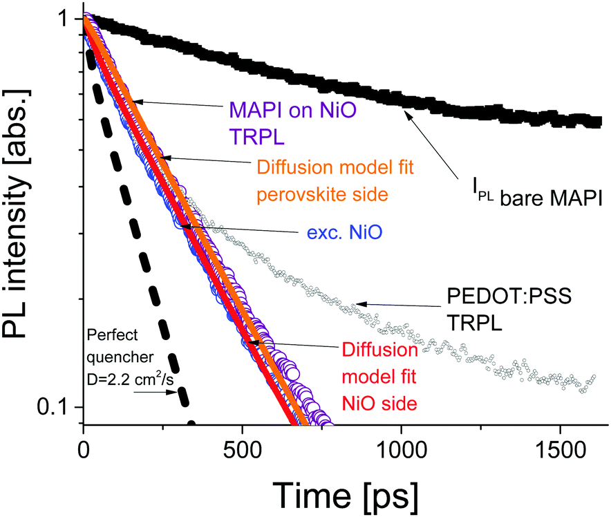 | ||
| Fig. 3 PL decays in bare perovskite film on glass (black squares) and quenched by NiO illuminated from the HEL side (blue circles) and perovskite side (purple circles). The diffusion model for perovskite side illumination is shown as the orange line and the substrate side model fit is shown as the red line. | ||
The PL decays in MAPbI3/NiO for the two illumination sides are very similar (Fig. 3). This suggests that photogenerated charges diffuse across the film rapidly, so that the rate of quenching is mostly determined by charge transfer to the HEL, rather than diffusion across the film to the HEL. The PL decays in MAPbI3/PEDOT:PSS measured after illumination from two sides are also very similar albeit they get substantially slower at higher excitation densities (Fig. S4, ESI†). This indicates that the extraction rate slows down when many holes are extracted to PEDOT:PSS and can be explained by Coulomb repulsion between the extracted holes and the holes accumulated at the MAPbI3/PEDOT:PSS interface.
A model based on the diffusion equation was used to simulate the spatio-temporal distribution of photogenerated holes within the perovskite layer and the integrated hole density over the thickness of the perovskite layer yielded the simulated PL decays shown in Fig. 3. The perfect quencher boundary condition was tested first and produced a good fit for the case of perovskite side illumination for the diffusion coefficient value of D = 1.06 cm2 s−1, however, the same perfect quencher model produces a large misfit when applied to the case where most charge carriers are created near the interface with the HEL [see Fig. S7, ESI†]. This is because a large proportion of holes would be immediately quenched in this case, leading to a pronounced fast PL decay. This emphasizes the importance of the two-side illumination approach as the issue with the perfect quenching model would not have been apparent without the substrate side illumination.
Imperfect quencher boundary condition on the other hand produces a good fit to both sets of experimental data with a single value of the diffusion coefficient, D = (2.2 ± 0.5) cm2 s−1 and quenching rate k = (3.6 ± 0.3) × 105 m s−1 [Fig. 3 and Fig. S8, ESI†]. Values of the diffusion coefficient outside of this range (larger or smaller) produce misfits which can be seen in Fig. S9 (ESI†). This result represents a significant improvement on the diffusion coefficient measurement technique as it allows for the determination of a relatively small range of values for the diffusion coefficient, taking into account a finite quenching velocity, rather than a lower limit on the diffusion coefficient as in the case of the perfect quencher assumption. We propose that all future surface quenching experiments for hybrid perovskites with high diffusion coefficients should be performed in this manner to avoid under-estimating the diffusion coefficient, as in this case the true value is about twice larger than that given by the perfect quencher model. Furthermore, quenching at the interface controls the concentration of diffusing species near that interface, which in turn is the primary driver behind diffusive transport. If the assumption of imperfect quenching does not reflect reality, the concentration gradient near the interface will be much smaller thus affecting transport. Our results demonstrate that the limiting factor in charge extraction in both cases is the transfer across the interface, even for the case of the superior HEL based on NiO nanoparticles. This insight would not have been revealed without the additional illumination from the substrate side. The PL decay simulated using the determined diffusion coefficient of D = 2.2 cm2 s−1 and the perfect quencher model is about twice faster than the measured decay [Fig. 3]. This shows that charge carriers could be extracted about twice as fast given the interfacial transfer rate was much faster. The high value of the diffusion coefficient is close to the values reported in single crystals6 suggesting that film quality does not suffer much because of using a solution processing method rather than a more complicated single crystal growth method.
We employed the imperfect quencher model to investigate hole extraction from CH3NH3PbI3/PEDOT:PSS (Fig. S10, ESI†) and using the same value of the diffusion coefficient as in CH3NH3PbI3/NiO we determined the quenching velocity. We find that it slows down by more than an order of magnitude within the same time window, in contrast to a constant quenching velocity for the case of CH3NH3PbI3/NiO. We attribute this slowing down of the rate to accumulation of holes on the CH3NH3PbI3/PEDOT:PSS interface. Further details of the fitting and analysis are provided in ESI.†
To investigate the charge diffusion regime, we carried out a charge density dependence study of the diffusion coefficient using the same surface quenching set-up. Measurements were performed at various excitation densities, revealing the role of charge density in the diffusion process. Fig. 4a shows the PL decays and (Fig. 4b) shows the extracted values of the diffusion coefficient as a function of charge density. The PL decays in bare MAPbI3/glass films and in the MAPbI3/NiO quenched films are independent of excitation density. For bare films this suggests that at the investigated charge densities the leading recombination process is due to monomolecular rather than bimolecular recombination, a result consistent with the low rates of bimolecular recombination reported by other researchers.17 The diffusion coefficient extracted from the PL decays on NiO shows no dependence on carrier density in the region of 1016–1017 cm−3 a result that can be identified as the band-like charge transport regime in perovskites.7 Even-though bimolecular recombination is identified as pertaining to the band-like transport regime it is still much slower in the case of our perovskite films than monomolecular recombination at the charge densities studied which is why the bulk recombination was modelled as monomolecular.
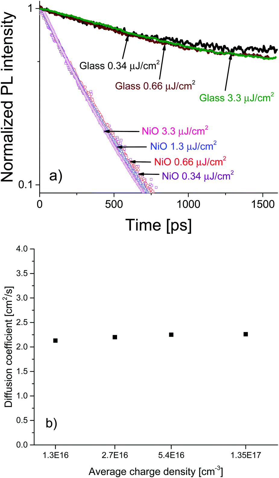 | ||
| Fig. 4 (a) PL decays of MAPbI3 films on glass, and on NiO. No dependence on excitation density is observed in the range 3.4 × 10⁻⁷ J cm−2 to 3.3 × 10⁻⁶ J cm−2. (b) Dependence of the diffusion coefficient D on the average density of charge pairs created as a result of the above laser illumination. | ||
The high and charge density independent value of the diffusion coefficient suggests high film quality with very low density of traps and a large proportion of mobile free charge carriers, previously reported only for perovskites grown by evaporation.7 Furthermore, the excitation density independent PL decays indicate that accumulation of charge is not an issue for the MAPbI3/NiO interface even at charge densities relevant to devices such as solar concentrator PVs. This is in contrast to the MAPbI3/PEDOT:PSS pair where the charge density dependence was observed. The almost identical PL decays observed after illumination from different sides strongly points towards this being an interface effect rather than a property of the bulk MAPbI3 perovskite. This further supports our claim that interfacial processes in devices based on perovskite active layers play a crucial role in the operation of those devices and should be the focus of future optimization efforts.
Conclusions
In summary, we designed a method based on the time resolved photoluminescence surface quenching experiment to unambiguously resolve bulk and interfacial effects on charge extraction from hybrid perovskites. We use this method to elucidate the limiting factors in hole extraction from CH3NH3PbI3 to two hole extracting layer materials, PEDOT:PSS and solution processed NiO nanoparticle film over a range of charge carrier densities relevant to solar cell operation. We find that NiO is the superior hole extracting layer, showing fast hole extraction on the timescale of 300 ps only slightly limited by transfer across the interface with the hole extracting layer. This is in contrast to PEDOT:PSS hole extracting layer which has a slower charge extraction which is severely limited by the rate of transfer across the interface. We attribute this worse performance to increased accumulation of holes at the CH3NH3PbI3/PEDOT:PSS interface. Furthermore, we determine the diffusion coefficient of holes in CH3NH3PbI3 to be (2.2 ± 0.5) cm2 s−1, one of the highest reported for solution processed hybrid perovskites. We find this diffusion coefficient to be independent of charge carrier density in the region of 1016–1017 cm−3 which is a hallmark of band-like transport, not observed in solution processed perovskites before. Our findings highlight the importance of separating the bulk and interfacial effects on charge extraction and show that charge carrier transfer across the interface is an important optimization parameter for perovskite solar cells.Conflicts of interest
There are no conflicts to declare.Acknowledgements
This work was supported by the Engineering and Physical Sciences Research Council (grant EP/L017008/1 and studentship grant EP/M508214/1 to O. Blaszczyk) and the European Research Council (grant 321305). Dr L. K. Jagadamma acknowledges support from a Marie Skłodowska-Curie Individual Fellowship (European Commission) (MCIF: No. 745776). The research data underpinning this publication can be accessed at DOI: https://doi.org/10.17630/902e94ee-cf79-4c1f-a48b-658115a059c5.Notes and references
- K. Galkowski, A. Mitioglu, A. Miyata, P. Plochocka, O. Portugall, G. E. Eperon, J. T.-W. Wang, T. Stergiopoulos, S. D. Stranks, H. J. Snaith and R. J. Nicholas, Energy Environ. Sci., 2016, 9, 962–970 RSC.
- A. Kojima, K. Teshima, Y. Shirai and T. Miyasaka, J. Am. Chem. Soc., 2009, 131, 6050–6051 CrossRef CAS PubMed.
- S. D. Stranks, S. D. Stranks, G. E. Eperon, G. Grancini, C. Menelaou, M. J. P. Alcocer, T. Leijtens, L. M. Herz, A. Petrozza and H. J. Snaith, Science, 2014, 342, 341–344 CrossRef PubMed.
- G. Xing, N. Mathews, S. Sun, S. S. Lim, Y. M. Lam, M. Gratzel, S. Mhaisalkar and T. C. Sum, Science, 2013, 342, 344–347 CrossRef CAS PubMed.
- R. L. Milot, G. E. Eperon, H. J. Snaith, M. B. Johnston and L. M. Herz, Adv. Funct. Mater., 2015, 25, 6218–6227 CrossRef CAS.
- P. Ščajev, C. Qin, R. Aleksiejunas, P. Baronas, S. Miasojedovas, T. Fujihara, T. Matsushima, C. Adachi and S. Juršėnas, J. Phys. Chem. Lett., 2018, 9, 3167–3172 CrossRef PubMed.
- P. Ščajev, R. Aleksiejunas, S. Miasojedovas, S. Nargelas, M. Inoue, C. Qin, T. Matsushima, C. Adachi and S. Juršenas, J. Phys. Chem. C, 2017, 121, 21600–21609 CrossRef.
- F. Thouin, D. A. Valverde-Chávez, C. Quarti, D. Cortecchia, I. Bargigia, D. Beljonne, A. Petrozza, C. Silva and A. R. Srimath Kandada, Nat. Mater., 2019, 18, 349–356 CrossRef CAS PubMed.
- W. S. Yang, B. Park, E. H. Jung and N. J. Jeon, Science, 2017, 356, 1376–1379 CrossRef CAS PubMed.
- E. Yalcin, M. Can, C. Rodriguez-Seco, E. Aktas, R. Pudi, W. Cambarau, S. Demic and E. Palomares, Energy Environ. Sci., 2019, 12, 230–237 RSC.
- L. K. Jagadamma, O. Blaszczyk, M. T. Sajjad, A. Ruseckas and I. D. W. Samuel, Sol. Energy Mater. Sol. Cells, 2019, 201, 110071 CrossRef.
- S. Kahmann and M. A. Loi, J. Mater. Chem. C, 2019, 7, 2471–2486 RSC.
- P. E. Shaw, A. Ruseckas and I. D. W. Samuel, Adv. Mater., 2008, 20, 3516–3520 CrossRef CAS.
- R. Kerremans, O. J. Sandberg, S. Meroni, T. Watson, A. Armin and P. Meredith, Sol. RRL, 2019, 1900221 CrossRef.
- A. B. Gregg, J. Sprague and M. W. Peterson, J. Phys. Chem. B, 1997, 101, 5249–5464 CrossRef.
- E. M. Y. Lee and W. A. Tisdale, J. Phys. Chem. C, 2015, 119, 9005–9015 CrossRef CAS.
- M. B. Johnston and L. M. Herz, Acc. Chem. Res., 2016, 49, 146–154 CrossRef CAS PubMed.
Footnote |
| † Electronic supplementary information (ESI) available. See DOI: 10.1039/c9mh01517e |
| This journal is © The Royal Society of Chemistry 2020 |