
 Open Access Article
 This Open Access Article is licensed under a
 Creative Commons Attribution 3.0 Unported Licence
Resonant doping for high mobility transparent conductors: the case of Mo-doped In2O3†
Jack E. N.
Swallow
 a,
Benjamin A. D.
Williamson
bc,
Sanjayan
Sathasivam
b,
Max
Birkett
a,
Thomas J.
Featherstone
a,
Philip A. E.
Murgatroyd
a,
Holly J.
Edwards
a,
Zachary W.
Lebens-Higgins
d,
David A.
Duncan
e,
Mark
Farnworth
f,
Paul
Warren
f,
Nianhua
Peng
g,
Tien-Lin
Lee
e,
Louis F. J.
Piper
d,
Anna
Regoutz
b,
Claire J.
Carmalt
b,
Ivan P.
Parkin
b,
Vin R.
Dhanak
a,
David O.
Scanlon
*bce and
Tim D.
Veal
*a
a,
Benjamin A. D.
Williamson
bc,
Sanjayan
Sathasivam
b,
Max
Birkett
a,
Thomas J.
Featherstone
a,
Philip A. E.
Murgatroyd
a,
Holly J.
Edwards
a,
Zachary W.
Lebens-Higgins
d,
David A.
Duncan
e,
Mark
Farnworth
f,
Paul
Warren
f,
Nianhua
Peng
g,
Tien-Lin
Lee
e,
Louis F. J.
Piper
d,
Anna
Regoutz
b,
Claire J.
Carmalt
b,
Ivan P.
Parkin
b,
Vin R.
Dhanak
a,
David O.
Scanlon
*bce and
Tim D.
Veal
*a
aDepartment of Physics and Stephenson Institute for Renewable Energy, University of Liverpool, Liverpool, L69 7ZF, UK. E-mail: T.Veal@liverpool.ac.uk
bDepartment of Chemistry, University College London, 20 Gordon Street, London, WC1H 0AJ, UK. E-mail: D.Scanlon@ucl.ac.uk
cThomas Young Centre, University College London, Gower Street, London WC1E 6BT, UK
dDepartment of Physics, Applied Physics and Astronomy, Binghamton University, Binghamton, New York 13902, USA
eDiamond Light Source, Harwell Science and Innovation Campus, Didcot, Oxfordshire OX11 0DE, UK
fNSG Group, European Technical Centre Hall Lane, Lathom, Ormskirk, Lancashire L40 5UF, UK
gSurrey Ion Beam Centre, University of Surrey, Surrey, GU2 7XH, UK
First published on 12th September 2019
Abstract
Transparent conductors are a vital component of smartphones, touch-enabled displays, low emissivity windows and thin film photovoltaics. Tin-doped In2O3 (ITO) dominates the transparent conductive films market, accounting for the majority of the current multi-billion dollar annual global sales. Due to the high cost of indium, however, alternatives to ITO have been sought but have inferior properties. Here we demonstrate that molybdenum-doped In2O3 (IMO) has higher mobility and therefore higher conductivity than ITO with the same carrier density. This also results in IMO having increased infrared transparency compared to ITO of the same conductivity. These properties enable current performance to be achieved using thinner films, reducing the amount of indium required and raw material costs by half. The enhanced doping behavior arises from Mo 4d donor states being resonant high in the conduction band and negligibly perturbing the host conduction band minimum, in contrast to the adverse perturbation caused by Sn 5s dopant states. This new understanding will enable better and cheaper TCOs based on both In2O3 and other metal oxides.
New conceptsA major challenge for research on transparent conducting oxides (TCOs) is to overcome the inherent limitations of the compromise between transparency and conductivity. Traditionally, n-type doping has used the element one to the right in the periodic table of the host cation or anion. In this work, we show that for the high carrier densities needed for TCOs, conventional dopants, such as tin in indium tin oxide (ITO), hybridize with the host conduction band states, increasing the band curvature and the band-edge effective mass and reducing the mobility. Particular transition metal dopants have long been known to result in higher electron mobilities, but the mechanism for this has not been clearly elucidated. Using the example of molybdenum doping of indium oxide, we show that the appropriate choice of transition metal dopant gives a d state donor level that is resonant with the conduction band, thereby avoiding the detrimental effects of donor states mixing with the CBM. Moreover, as well as giving computational and spectroscopic evidence of the resonant doping phenomena, the enhanced doping behaviour is rationalised by invoking crystal field theory for the Mo 4d dopant states and emphasizing the role of the positive charge state of the dopant ion that has previously been overlooked. This new understanding paves the way for the realization of high performance TCOs. |
Introduction
Transparent conducting oxides (TCO) combine the usually mutually exclusive properties of electrical conductivity and optical transparency, making their use ubiquitous in consumer electronics and glass coatings.1,7 The global TCO market is predicted to have an annual growth rate exceeding 17%, reaching $8.04 billion by 2022.8 The demand for higher conductivities and the volatile and high price of indium has led to the search for new TCO materials. However, as shown in Fig. 1, alternative indium-free TCOs such as graphene, carbon nanotubes and oxide/metal/oxide layers have failed to surpass or even reach ITO's performance;1,9,10 ITO continues to account for 60% of the transparent conductor market and 60% of global indium use.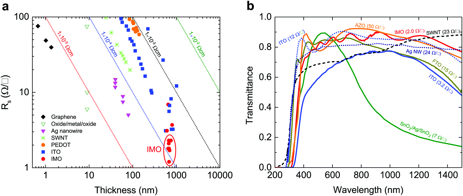 | ||
| Fig. 1 Sheet resistances and optical transmittances of transport conducting electrodes. (a) Sheet resistance Rs as a function of film thickness for different transparent conducting films:1 PEDOT-PSS;2 ITO films;3,4 SWNTs;3 Ag nanogrid;3 oxide/Ag/oxide films;5 and graphene.3 This figure is based on Ellmer's1 with data points for IMO added and highlighted by the red ellipse. The IMO films have the lowest sheet resistances. The dotted diagonal lines denote constant resistivity values. (b) Spectral transmission of different transparent electrode films: single walled carbon nanotubes (SWNT) (23 Ω □−1), Ag nanowires (24 Ω □−1), aluminium-doped ZnO (AZO, 50 Ω □−1), ITO (12 Ω □−1),5 SnO2/Ag/SnO2 (7 Ω □−1),6 compared with our measurements of IMO (2 Ω □−1), ITO (3.2 Ω □−1), and fluorine-doped SnO2 (FTO, 15 Ω □−1). All materials which approach IMO's sheet resistance have much inferior infrared transparency. | ||
Given this failure of the alternative transparent conductors, it is remarkable that In2O3 doped instead with molybdenum, giving double the conductivity of ITO, has not been adopted by industry in spite of first being suggested over 15 years ago. Reports of Mo-doped In2O3 have been sporadic and have contained little insight into the origins of its superior performance. In fact, reports of IMO showing promising performance seem to have been treated merely as a curiosity, and thus IMO was never identified as a research direction deserving of further detailed investigation. Perhaps this lack of research and dearth of understanding has prevented industry overcoming its inertia to substitute an established high performing material for a significantly better one. Here we present a comprehensive explanation of why IMO outperforms ITO. This work opens the pathway for immediate commercial adoption of IMO, and for the development of other high performing TCOs.
Results
Mo universally delivers higher conductivity than Sn in In2O3
Comparing Mo and Sn dopants in In2O3 (Fig. 2), we find that higher mobilities and lower resistivities are universally obtained with Mo. Fig. 2, which shows the Van der Pauw resistivity and mobility as a function of carrier concentration, includes data from our chemical vapour-deposited films as well as those from other studies of IMO and ITO. X-ray diffraction (Fig. S1a, ESI†) confirmed the cubic bixbyite structure of the films. Film thickness varied from 670–800 nm for IMO and 700–1600 nm for ITO as determined by cross-sectional scanning electron microscopy (Fig. S1b, ESI†). Calibrated secondary ion mass spectrometry (Fig. S2, ESI†) indicates that the dopant concentrations are the same as the free electron densities, implying that within the uncertainty there is one free electron per Mo atom in IMO and Sn atom in ITO. For IMO, a resistivity as low as 0.8 × 10⁻⁴ Ω cm has been achieved, almost half of the 1.4 × 10⁻⁴ Ω cm for ITO. This is enabled by IMO's extremely high mobilities displayed in Fig. 1b. Mo clearly outperforms Sn as a dopant, with IMO films having mobilities of up to 150 cm2 V−1 s−1 compared with the 80 cm2 V−1 s−1 for ITO. Table S1, ESI† provides further details of electronic and optical properties. From all available results, a trend of twice the conductivity for IMO over ITO of the same carrier concentration is apparent. Therefore only half the amount of indium is required for IMO films with both better optical properties and improved conductivity over ITO, giving potentially huge savings in materials and costs.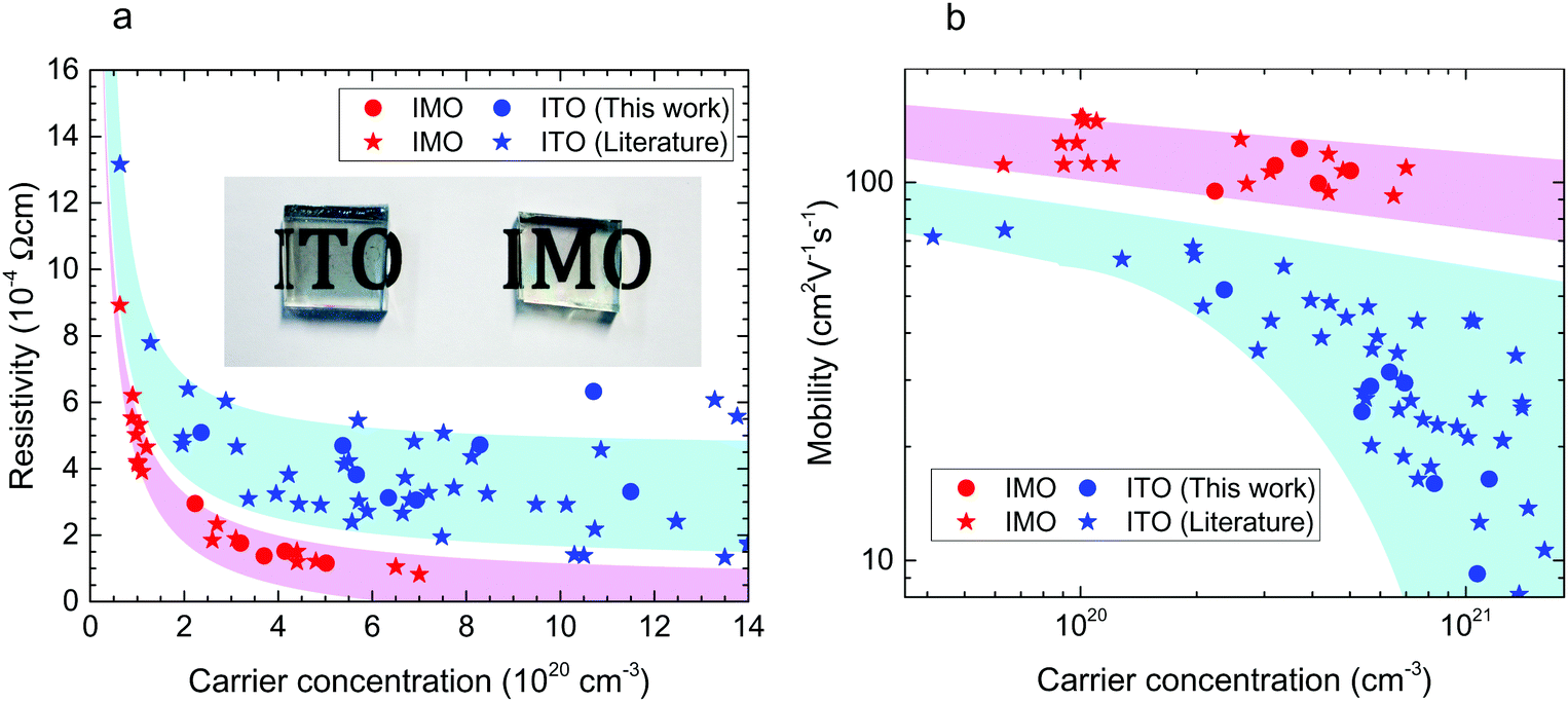 | ||
| Fig. 2 Transport properties. (a) Resistivity versus free carrier concentration for polycrystalline ITO and IMO films. Inset shows a photograph of ITO and IMO films. (b) Hall mobility versus free carrier concentration. Data from this work are circles. Data plotted as stars are taken from the literature for IMO11–16 and ITO12,17–22 films. In this carrier concentration regime, the electron mobility is limited by ionized impurity scattering. | ||
Conventional dopants impair mobility due to state mixing with host CBM
The main factor that limits the properties of TCOs is the trade-off between doping for increased conductivity and consequential decrease in optical transparency due to band tailing and the raised conduction electron plasma energy. Optical transmission spectra of IMO and ITO (Fig. 3a) show that IMO generally has greater transmission at 550 nm (2.25 eV), where the human eye is most sensitive (see also Table S1, ESI†). Optical absorption spectra of IMO and ITO (Fig. S3, ESI†) show similar optical band gaps (via the method of Dolgonos et al.23), yet the conduction electron plasma edge from infrared reflectivity lies at strikingly lower energies in IMO, greatly enhancing transparency (see also Fig. 3a). Plasma frequency relates to carrier density and effective mass as ωp2 ∝ n/〈m*〉 and so these data indicate an inherent difference in the effective masses of conduction electrons between In2O3 doped with Sn and Mo, diverging from the commonly accepted rigid band model of doping.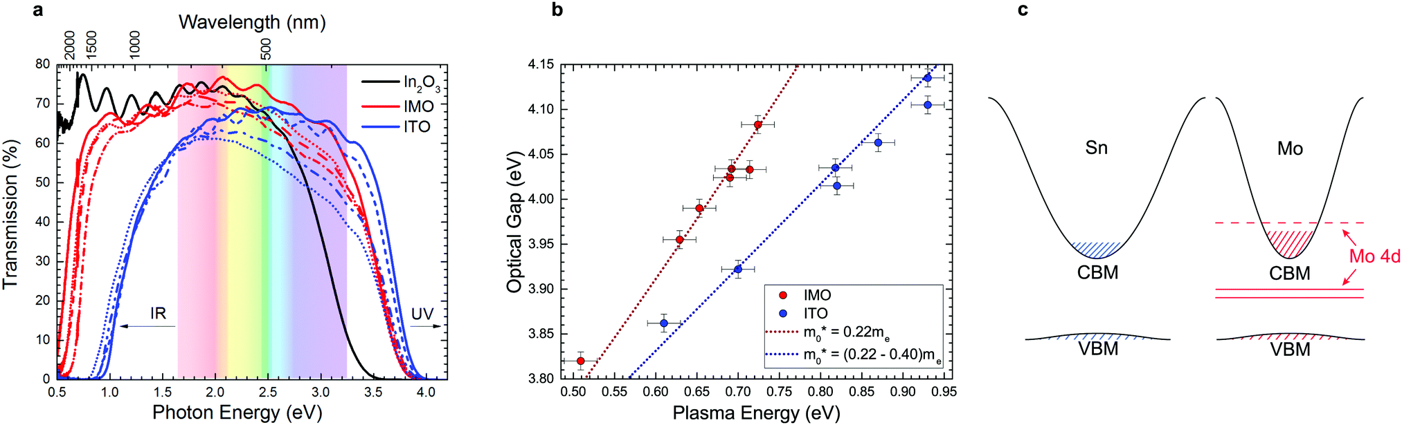 | ||
| Fig. 3 Optical transmission and associated properties. (a) Optical transmission of IMO and ITO films (on 3.6 mm-thick soda lime glass) with a range of carrier concentrations, and a nominally undoped In2O3 film, revealing greatly enhanced transparency in IMO due to plasma edges lying at lower energies. (b) Optical gap versus plasma edge energy of IMO and ITO films, the steeper gradient for IMO indicates a (highly desirable) reduced conduction band minimum effective mass with respect to that of ITO. Model curve lines are calculated using Fermi statistics with a density-of-states averaged effective mass. (c) Schematic representation of the band structure of ITO (left) and IMO (right) with the same carrier concentration. The IMO has a narrower conduction band dispersion with lower band edge effective mass than ITO and so a higher Fermi level is required to obtain the same number of states as in ITO. In IMO, the resonant and midgap Mo 4d bands are shown, respectively, by the dashed and solid red lines. No Sn state is shown in the ITO band structure schematic as the Sn 5s states mix with the states of the conduction band. | ||
The red-shifted IMO plasma edges are understood after plotting optical gap versus plasma energy in Fig. 3b. Both the IMO and ITO optical gaps increase monotonically with plasma energy due to band filling; however, the steeper IMO curve indicates a desirably reduced electron effective mass (a similar dependence holds between optical gap and carrier density in Fig. S4a, ESI†). This effect is modelled in Fig. 3b using carrier statistics (as described in the ESI†). The conduction band minimum (CBM) or band edge effective mass used is 0.22me as determined previously from angle resolved photoemission and density functional theory (DFT) calculations.24–26 Modelling of the ITO data required a deviation from the rigid band model by increasing the band edge effective mass incrementally with Sn-content from 0.22me to 0.40me (in excellent agreement with previous theoretical predictions ref. 25). The carrier density-dependence of the effective mass for IMO and ITO is shown in Fig. S4b, ESI.† The correspondingly different conduction band dispersions in heavily doped IMO and ITO are shown schematically in Fig. 3c. The increasing band edge effective mass in ITO is consistent with the additional decrease in mobility as carrier concentration increases as seen in Fig. 2b and modelled in Fig. S3c, ESI.† In contrast to ITO, the IMO data in Fig. 3b is well reproduced using a fixed band edge effective mass of 0.22me for all Mo concentrations.
Mo dopant states lie at favourable energies in In2O3
The undoped In2O3 and IMO band structures calculated using density functional theory (DFT) using 80 atom unit cells are shown in Fig. 4a and b. For IMO, one indium atom is replaced by one Mo atom, corresponding to a Mo concentration of 3.125% of the cations. Mo 4d levels in IMO are energetically separated from the CBM and do not mix readily with the In 5s–O 2p-dominated CBM. The Mo 4d levels can be seen as mid-gap states and as a donor state resonant in the conduction band in the calculated band structure (Fig. 4b). Mo states mix minimally with those of the In2O3 CBM; in contrast Sn states strongly perturb the CBM. This is supported by Fig. 4c–f, which depict the DFT-calculated partial charge densities. At the CBM, whilst the IMO electron density is delocalised across the lattice, minimal density exists near the Mo (green) atom (Fig. 4d); in contrast, considerable density exists across the ITO lattice, including around the Sn (red) atom (Fig. 4f). The Sn 5s states hybridize with the In 5s/O 2p character CBM.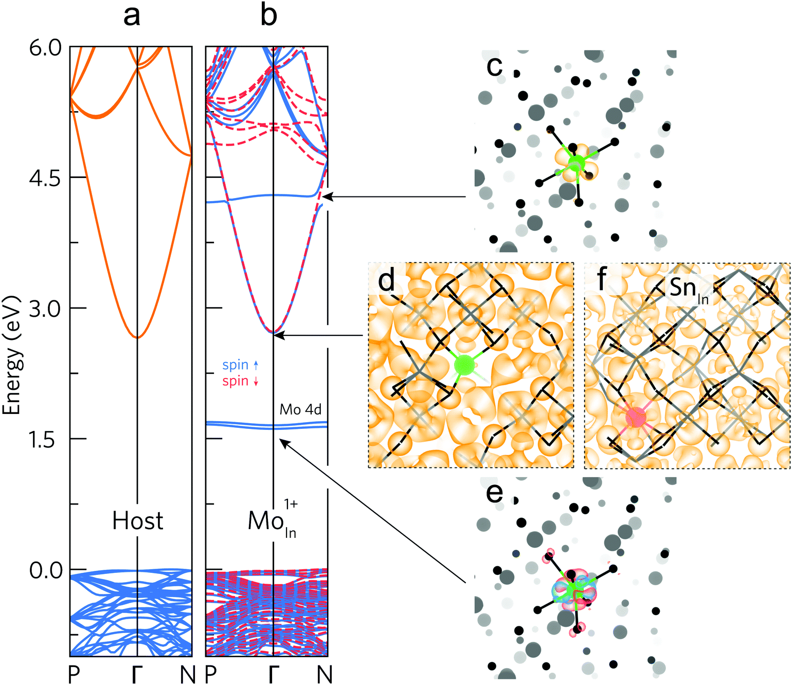 | ||
| Fig. 4 Band structures and partial charge densities. (a) and (b) Band structures for undoped In2O3 and for IMO, including both spin components, with the Mo donor in the ionized 1+ charge state. The zero of the energy scale is the VBM. (c)–(e) show the partial charge densities for IMO corresponding to the resonant state in the conduction band, at the CBM and for the two states in the band gap respectively. (f) The partial charge density at the CBM is also shown for ITO. The Mo24dIn atom is green, the Sn8bIn atom is red and the In2O3 lattice is portrayed using a wireframe. For the resonant state and the midgap states, the O and In atoms are shown by black and grey spheres and the ‘bonds’ on the In2O3 lattice are removed in order to clearly visualise the MoO6 distorted octahedra. | ||
The Mo 4d states are depicted schematically in Fig. 5a and are observed in the photoemission and inverse photoemission spectra shown in Fig. 5b. Conduction band photoemission shown in Fig. 5c directly evidences the different conduction band dispersion for IMO and ITO discussed above. (See also Fig. S5, ESI† and associated descriptions of additional photoemission and X-ray absorption data.) While the midgap states might be thought to impair transparency, this is shown not to be the case from the transmission data in Fig. 3. This is because optical transitions to and from the midgap Mo 4d states have only minimal dipole intensity.
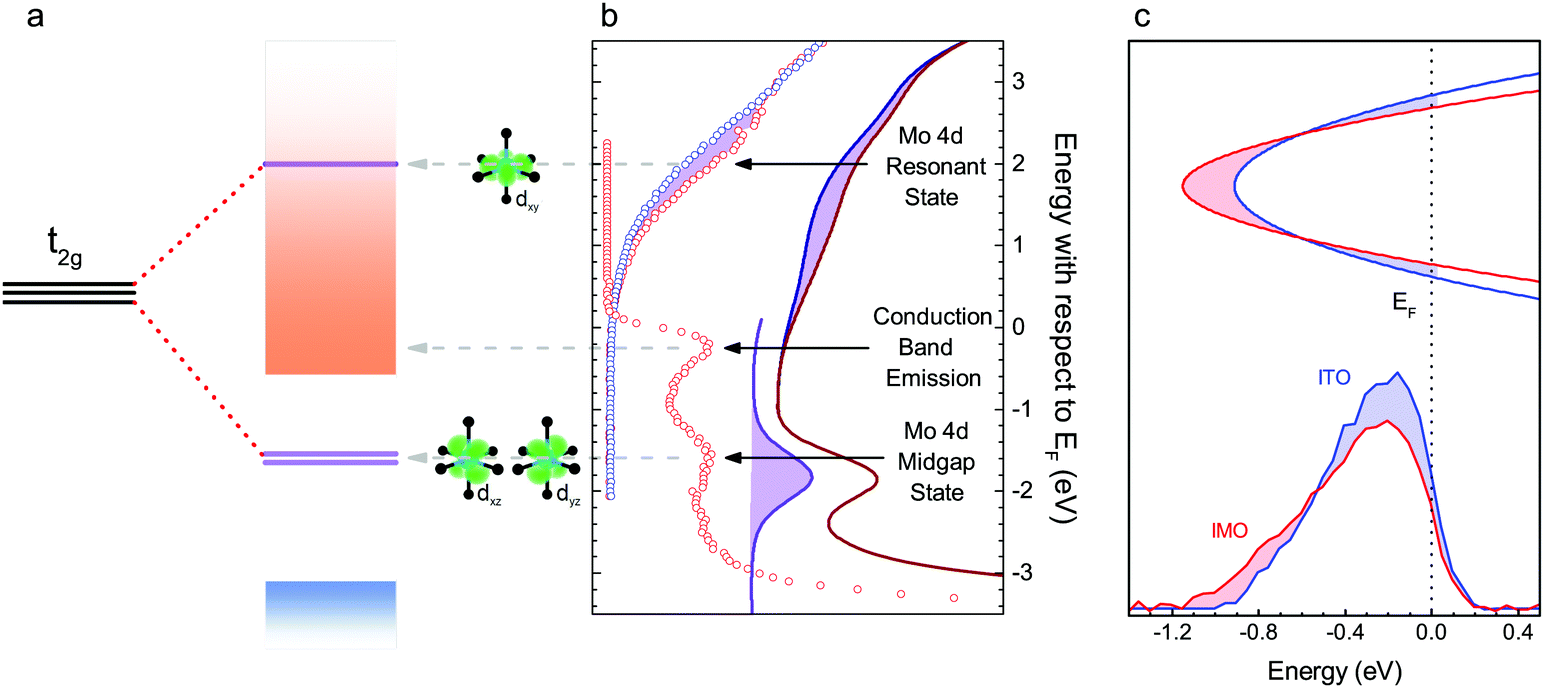 | ||
| Fig. 5 Spectroscopy of electronic structure. a Schematic diagram of Mo 4d t2g states and their corresponding orbitals (depicted in green), splitting into the upper state, dxy, resonant with the conduction band (orange shading), the two lower states, dxz and dyz, in the band gap and the valence band (blue shading). The splitting resulting from tetrahedral elongation Jahn–Teller distortion of the MoO6 octahedron is shown for comparison with the highly distorted Mo24dIn depicted in Fig. 4. (b) Inverse photoemission data from ITO (blue) and IMO (red), showing extra intensity in the IMO data, corresponding to an unoccupied Mo 4d state resonant with the conduction band. Also shown is high energy photoemission data of the conduction band emission, Mo 4d midgap states and valence band onset of IMO. The features in part (a) of the figure are aligned to the corresponding peaks in the spectra. (c) Schematic band diagram, showing wavevector (vertical axis) versus energy (horizontal axis) representing the conduction bands of similarly doped IMO (red) and ITO (blue) aligned to the Fermi level. Below are background subtracted HAXPES spectra displaying conduction band emission from IMO (red, n = 5.0 × 1020 cm−3) and ITO (blue, n = 6.3 × 1020 cm−3). The spectra are normalised to the In 5s-dominated valence band peak at −9 eV. The shaded regions emphasise the additional intensity of the ITO peak and additional width of the IMO peak. | ||
Why Mo 4d states are at favourable energies
To explain why Mo in In2O3 has two occupied 4d states within the band gap and one donor state resonant with the conduction band, we consider the electronic structure and crystal field environment of Mo in In2O3. Mo and Sn have respective electron configurations of [Kr]4d55s1 and [Kr]4d105s25p2, while bixbyite cubic In2O3 has two distinct indium sites: the 8b and 24d Wyckoff sites, with respective regular and tetragonally-distorted octahedral crystal environments. At an indium site, three electrons participate in bonding, leaving Sn or Mo respectively in a [Kr]4d105s1 or [Kr]4d3 configuration, that is one Sn 5s or three Mo 4d as the outermost electrons. At Fermi levels matching experiments (around VBM + 3.3 eV) Sn or Mo preferentially substitute on the respective 8b or 24d sites (each donating one conduction electron), whilst Mo8bIn has a neutral charge state (donating no carriers), see Fig. S6, ESI.† The Jahn–Teller-like distortion at the 24d site splits the three-fold degenerate t2g levels (valid for octahedral symmetry), shifting the dxy orbital up in energy to the vicinity of the CBM, and dxz and dyz down into the gap, as shown in the unfolded band structures for the neutral charge state (Mo24dInq = 0) in Fig. S7, ESI.† If all Mo 4d states lie below the CBM (as reported elsewhere from calculations),27 then no effective doping would occur at room temperature; the experimental results shown in Fig. 2 clearly rule this out. If the highest occupied Mo 4d state lies just above the CBM (reported elsewhere),12 it would merge with the occupied CBM, increasing the electron effective mass and reducing mobility, and the Fermi level would be pinned by the partially occupied 4d state.Both previous works fail to consider Mo atoms in a +1 charge state,12,27 which increases the distortion of the octahedra and the splitting of the t2g-derived 4d energy levels, making the dxy orbital resonant with the conduction band. This contributes a conduction electron without detrimental hybridization with the CBM states; whilst the singly-occupied dxz and dyz orbitals are stabilized by the bond length contraction and pushed deeper into the band gap (see Mo24dInq = +1 in Fig. S7, ESI†). A schematic representation of this t2g level splitting is shown in Fig. 5a along with partial electron densities for the dxy, dxz, and dyz orbitals (full schematic molecular orbital diagrams for MoO6 octahedra are shown in Fig. S8, ESI†). Indeed, the calculated partial electron charge densities around the Mo atom at the resonant Mo level (Fig. 4c) and two mid-gap levels (Fig. 4e) show clear similarities respectively to the schematic dxy, and a combination of the dxz and dyz orbitals of Fig. 5a. This picture of the Mo 4d state energies in IMO is further corroborated by additional confidence in the calculated results coming from comparisons of the bond lengths from calculations and those determined from extended X-ray absorption fine structure measurements (see Fig. S9, ESI† and related discussion).
IMO is as durable as ITO
The durability of our CVD IMO films has been compared to that of both our CVD ITO films and commercial ITO films. This was done by measuring the sheet resistance and transmission before and after tape, scratch, heat and acid tests, as shown in Fig. S10, ESI.† IMO films were found to be as durable as the ITO films.Design criteria established for high mobility TCOs
Beyond having a transformative impact by replacing the ubiquitous ITO with better and cheaper IMO, this work enables design criteria for other high mobility TCOs to be established: (1) transition metal dopants are required so that their donor d states hybridize minimally with the host cation s states of the CBM, avoiding problems inherent with conventional s level dopants; (2) the transition metal dopant atoms must possess d orbital energy levels such that the dopant is a singly charged donor to minimize mobility-reducing ionized impurity scattering; and (3) the donor level must be resonant within the conduction band to avoid a high effective mass, low mobility d state at or close to the CBM.No barrier to ITO being replaced by cheaper, better IMO
IMO is an optically and electronically superior material to the commercially-dominant transparent electrode, ITO. This makes IMO not only more suited for the many diverse applications that ITO is currently used for, but also implies enormous potential for industrial cost savings as much thinner films of IMO can be produced with properties equal to or better than ITO of the same carrier concentration. We have combined theory and experiment to explore the reasons for the drastic differences between these two In2O3-based TCOs. The rigid band model fails to describe the variation of optoelectronic properties of ITO with doping concentration. For heavy Sn-doping, the role of the Sn 5s states in perturbing the host In2O3 conduction band and increasing the band edge effective mass must be included to describe both the evolution of optical gap and mobility with doping. Having identified this shortcoming of ITO, we show that this is avoided by instead using Mo as the dopant. The different energetic position and atomic orbital character of Mo states compared with those of Sn means that negligible hybridization between Mo states and the CBM occurs. These findings provide a new immediately viable and durable alternative to ITO, the industry standard TCO. While Mo and Sn are similarly priced, IMO films with half the thickness offer huge cost savings over ITO films of the same sheet resistance. Moreover, the understanding presented will enable the design of other TCO materials and dopants with improved transparent conducting properties.Methods
Material fabrication
We prepared nominally undoped, Mo-doped and Sn-doped In2O3 films deposited on SiO2 coated (50 nm sodium diffusion barrier) soda-lime glass (NSG) via AACVD using a cold-wall horizontal gas flow reactor. Precursors and solvents were procured from Aldrich and used as received. These consisted of InCl3H2O (0.2 g, 4.4 mmol) dissolved in methanol (20 mL). (NH4)6Mo7O24·4H2O was incorporated with a range of 1–7 mol% for Mo-doped films and C4H9SnCl3 with a range of 0.5–5 mol% for Sn-doped films. The precursor–solvent mixtures were ultrasonicated for 10 min to help precursors dissolve before the resulting homogeneous solutions were atomized to create an aerosol mist using a piezoelectric device. The N2 carrier gas flow was held at 0.6 L min−1 and the substrate temperature was maintained at 450 °C. All films were transparent, well adhered to the substrate and stable in air. Film durability was tested and compared to that of CVD ITO and commercial ITO coated glass (see Fig. S10, ESI†) which proved comparable. IMO film thicknesses ranged from 670–800 nm while ITO films ranged from 700–1600 nm.Material characterisation
Film thickness was determined by cross sectional scanning electron microscopy (SEM) using a JEOL JSM-6301F field emission SEM at an accelerating voltage of 5 kV. Hall effect measurements (for the determination of resistivity ρ, charge carrier mobility μ and free carrier concentration n) were performed at room temperature with a Keithley 2182A nanovoltmeter and 6220 current source at a maximum field strength of 0.8 T in the van der Pauw geometry. Infrared (IR) reflectance measurements were performed using a Bruker Vertex 70v Fourier transform infrared spectrometer. All measurements were performed at 45° angle of incidence, utilising the Pike Veemax II accessory, and S-polarising filter. All FTIR measurements were performed with a near-IR light source, CaF2 beam splitter and DLaTGS detector. Transmission measurements were obtained with use of a Shimadzu UV-Vis-IR 3700 spectrophotometer with an integrating sphere detector. Hard X-ray photoelectron spectroscopy was performed at the I09 beamline at Diamond Light source. Measurements were performed at both 6.45 keV and 2.15 keV for different depth dependence. Photoelectrons were collected and analysed using a SCIENTA EW-4000 electron energy analyser. The sample was irradiated in grazing incidence geometry, that is an angle of ∼3° between X-ray beam and sample surface. The energy calibration and resolution of the system were determined from a polycrystalline Au foil. The energy resolution was determined by fitting a Gaussian–Fermi function convolution to the Fermi edge, and was found to be 300 meV. Inverse photoemission spectroscopy measurements were performed using a PSP Vacuum Technology BaO cathode dispenser electron source and an isochromat NaCl photon detector, both at 45° to the sample normal. Energy calibration was performed using the known energy position of the lowest occupied molecular orbital of multilayer C60 deposited in situ and the spectrometer resolution determined from a polycrystalline Au foil was 1.27 eV. The IMO and ITO samples were annealed to 300 °C for 2 hours in preparation for IPES measurement.Theoretical and modelling methods
Hybrid density functional theory (DFT) calculations were carried out on In2O3 using a plane-wave basis within the periodic code, VASP.28–31 We employ a screened non-local exchange–correlation density functional (HSE06).32 The projector augmented wave method (PAW)33 was used to describe the core and valence electrons interaction. Full details of the calculations performed are provided in the ESI.† The band unfolding code BandUp was used to obtain a primitive cell representation of the band structure.34,35Sample plasma energies were extracted from IR reflectivity measurements utilizing a two-oscillator dielectric model36 and transfer matrix method for optical simulation.37 A four layer (vacuum/In2O3/SiO2/soda-lime glass) stratified medium was used in the model, with complete incoherence being assumed in the glass substrate and partial incoherence in the vacuum/In2O3 interface. The absorption spectra were calculated from the transmission spectra of the samples using the Beer–Lambert relation. Optical gaps were extracted from the absorption spectra using a method proposed by Hamberg,38 illustrated by Dolgonos et al.23 which better accounts for degeneracy in materials compared to the more common Tauc analysis. A carrier statistics model was used in order to relate optical gap and plasma energy through the density-of-states average effective mass.
Author contributions
TDV and DOS devised the study. JENS, BADW and TDV wrote the manuscript with input from PAEM, MB and DOS. SS, CJC and IPP designed the sample growth that was performed by SS. JENS, AR, TJF, HJE, DAD and T-LL performed the HAXPES measurements which were analysed by JENS with input from TDV and VRD. JENS performed and analysed the IPES measurements with input from TDV and VRD. ZWL-H and LFJP performed and analysed the XAS measurements. MF and PW performed the SIMS measurements and analysed the data with JENS and TDV. NP performed the ion implantation of the SIMS standards. XRD was performed by TJF. SEM was performed by SS. The optical and transport measurements were performed by JENS, MB and SS, and analysed and modelled by JENS, with input from MB and TDV. BADW and DOS performed the first principles calculations and analysed the results. The authors contributed to the scientific discussion and edited the manuscript.Conflicts of interest
The authors declare that two authors (MF and PW) are affiliated to NSG Group which manufactures and sells TCO-coated glass.Acknowledgements
This work was supported by the Engineering and Physical Sciences Research Council (EPSRC) (Grant No. EP/N01572X/1 and EP/N015800/1) and the Leverhulme Research Centre for Functional Materials Design. J. E. N. S. and T. J. F. acknowledge studentship support from the EPSRC Centre for Doctoral Training in New and Sustainable Photovoltaics (Grant No. EP/L01551X/1). The XRD facility used was supported by EPSRC (Grant No. EP/P001513/1). BADW and DOS acknowledge the UK Materials and Molecular Modelling Hub for computational resources, which is partially funded by EPSRC (EP/P020194/1). This work made use of the ARCHER UK National Supercomputing Service (http://www. archer.ac.uk) via the authors’ membership of the UK's HEC Materials Chemistry Consortium, which was funded by EPSRC (EP/L000202/1). The UCL Legion and Grace HPC Facilities (Legion@UCL and Grace @UCL) were also used in the completion of this work. A. R. acknowledges support her Imperial College Research Fellowship. S. S. thanks Dr Davinder S. Bhachu and Dr Chris S. Blackman for useful discussions. The authors thank Diamond Light source for providing beam time and facilities under SI18428-1 and David McCue for technical assistance. D. O. S. and T. D. V. acknowledge membership of the Materials Design Network. This research used beamline 23-ID of the National Synchrotron Light Source II, a U.S. Department of Energy (DOE) Office of Science User Facility operated for the DOE Office of Science by Brookhaven National Laboratory under Contract No. DE-SC0012704. The Binghamton work is supported by the Air Force Office of Scientific Research under award number FA9550-18-1-0024.References
- K. Ellmer, Nat. Photonics, 2012, 6, 809–817 CrossRef CAS
.
- Y. H. Kim, C. Sachse, M. L. Machala, C. May, L. Müller-Meskamp and K. Leo, Adv. Funct. Mater., 2011, 21, 1076–1081 CrossRef CAS
- F. Bonaccorso, T. H. Z. Sun and A. C. Ferrari, Nat. Photonics, 2010, 4, 611–622 CrossRef CAS
- D. B. Fraser and H. D. Cook, J. Electrochem. Soc., 1972, 119, 1368–1374 CrossRef CAS
- T. M. Barnes, M. O. Reese, J. D. Bergeson, B. A. Larsen, J. L. Blackburn, M. C. Beard, J. Bult and J. van de Lagemaat, Adv. Energy Mater., 2012, 2, 353–360 CrossRef CAS
- J. Szczyrbowski, A. Dietrich and K. Hartig, Sol. Energy Mater., 1989, 19, 43–53 CrossRef CAS
- M.-G. Kim, M. G. Kanatzidis, A. Facchetti and T. J. Marks, Nat. Mater., 2011, 10, 382–388 CrossRef CAS
- Transparent Conductive Films Market By Application Type (Smartphones, Tablets, Notebooks, LCDs, Wearable Devices); On the basis of Material (ITO on Glass, ITO on PET, Silver Nanowires, Metal Mesh, Carbon Nanotubes) and by Regional Analysis – Global Forecast, 2017.
- A. Kumar and C. Zhou, ACS Nano, 2010, 4, 11–14 CrossRef CAS PubMed
- L. Zhang, Y. Zhou, L. Guo, W. Zhao, A. Barnes, H. T. Zhang, C. Eaton, Y. Zheng, M. Brahlek, H. F. Haneef, N. J. Podraza, M. H. Chan, V. Gopalan, K. M. Rabe and R. Engel-Herbert, Nat. Mater., 2016, 15, 204–210 CrossRef CAS PubMed
- S. Parthiban, E. Elangovan, K. Ramamurthi, R. Martins and E. Fortunato, Sol. Energy Mater. Sol. Cells, 2010, 94, 406–412 CrossRef CAS
- D. S. Bhachu, D. O. Scanlon, G. Sankar, T. D. Veal, R. G. Egdell, G. Cibin, A. J. Dent, C. E. Knapp, C. J. Carmalt and I. P. Parkin, Chem. Mater., 2015, 27, 2788–2796 CrossRef CAS
- Y. Meng, X. Yang, H. Chen, J. Shen, Y. Jiang, Z. Zhang and Z. Hua, Thin Solid Films, 2001, 394, 218–223 CrossRef
- S. Parthiban, K. Ramamurthi, E. Elangovan, R. Martins and E. Fortunato, Appl. Phys. Lett., 2009, 94, 212101 CrossRef
- N. Yamada, M. Yamada, H. Toyama, R. Ino, X. Cao, Y. Yamaguchi and Y. Ninomiya, Thin Solid Films, 2017, 626, 46–54 CrossRef CAS
- Y. Meng, X.-l. Yang, H.-x. Chen, J. Shen, Y.-m. Jiang, Z.-j. Zhang and Z.-y. Hua, J. Vac. Sci. Technol., A, 2002, 20, 288–290 CrossRef CAS
- R. B. H. Tahar, T. Ban, Y. Ohya and Y. Takahashi, J. Appl. Phys., 1998, 83, 2631–2645 CrossRef
- R. Groth, Phys. Status Solidi, 1966, 14, 69–75 CrossRef CAS
- M. Mizuhashi, Thin Solid Films, 1980, 70, 91–100 CrossRef CAS
- R. Clanget, Appl. Phys., 1973, 2, 247–256 Search PubMed
- P. K. Song, Y. Shigesato, M. Kamei and I. Yasui, Jpn. J. Appl. Phys., 1999, 38, 2921–2927 CrossRef CAS
- Y. Shigesato, S. Takaki and T. Haranoh, J. Appl. Phys., 1992, 71, 3356–3364 CrossRef CAS
- A. Dolgonos, T. O. Mason and K. R. Poeppelmeier, J. Solid State Chem., 2016, 240, 43–48 CrossRef CAS
- K. H. L. Zhang, R. G. Egdell, F. Offi, S. Iacobucci, L. Petaccia, S. Gorovikov and P. D. C. King, Phys. Rev. Lett., 2013, 110, 056803 CrossRef CAS
- A. Walsh, J. L. F. Da Silva and S.-H. Wei, Phys. Rev. B: Condens. Matter Mater. Phys., 2008, 78, 075211 CrossRef
- F. Fuchs and F. Bechstedt, Phys. Rev. B: Condens. Matter Mater. Phys., 2008, 77, 155107 CrossRef
- J. Xu, J.-B. Liu, B.-X. Liu, S.-N. Li, S.-H. Wei and B. Huang, Adv. Electron. Mater., 2018, 4, 1700553 CrossRef
- G. Kresse and J. Hafner, Phys. Rev. B: Condens. Matter Mater. Phys., 1994, 49, 14251–14269 CrossRef CAS
- G. Kresse and J. Hafner, Phys. Rev. B: Condens. Matter Mater. Phys., 1993, 47, 558–561 CrossRef CAS PubMed
- G. Kresse and J. Furthmüller, Comput. Mater. Sci., 1996, 6, 15–50 CrossRef CAS
- G. Kresse and J. Furthmüller, Phys. Rev. B: Condens. Matter Mater. Phys., 1996, 54, 11169–11186 CrossRef CAS PubMed
- A. V. Krukau, O. A. Vydrov, A. F. Izmaylov and G. E. Scuseria, J. Chem. Phys., 2006, 125, 224106 CrossRef
- P. E. Blöchl, Phys. Rev. B: Condens. Matter Mater. Phys., 1994, 50, 17953–17979 CrossRef
- P. V. C. Medeiros, S. Stafström and J. Björk, Phys. Rev. B: Condens. Matter Mater. Phys., 2014, 89, 041407 CrossRef
- P. V. C. Medeiros, S. S. Tsirkin, S. Stafström and J. Björk, Phys. Rev. B: Condens. Matter Mater. Phys., 2015, 91, 041116 CrossRef
- C. Pickering, J. Phys. C: Solid State Phys., 1980, 13, 2959–2968 CrossRef CAS
- C. C. Katsidis and D. I. Siapkas, Appl. Opt., 2002, 41, 3978–3987 CrossRef
- I. Hamberg, C. G. Granqvist, K. F. Berggren, B. E. Sernelius and L. Engström, Phys. Rev. B: Condens. Matter Mater. Phys., 1984, 30, 3240–3249 CrossRef CAS
Footnote |
| † Electronic supplementary information (ESI) available. See DOI: 10.1039/c9mh01014a |
| This journal is © The Royal Society of Chemistry 2020 |