
 Open Access Article
 This Open Access Article is licensed under a
 Creative Commons Attribution 3.0 Unported Licence
Generating semi-metallic conductivity in polymers by laser-driven nanostructural reorganization†
Changhun
Yun
 a,
Joo Won
Han
b,
Soyeon
Kim
c,
Dong Chan
Lim
c,
Hyunsu
Jung
a,
Seung-Hoon
Lee
d,
Jae-Won
Jang
d,
Seunghyup
Yoo
e,
Karl
Leo
f and
Yong Hyun
Kim
*b
a,
Joo Won
Han
b,
Soyeon
Kim
c,
Dong Chan
Lim
c,
Hyunsu
Jung
a,
Seung-Hoon
Lee
d,
Jae-Won
Jang
d,
Seunghyup
Yoo
e,
Karl
Leo
f and
Yong Hyun
Kim
*b
aCenter for Nano-Photonics Convergence Technology, Korea Institute of Industrial Technology (KITECH), Gwangju 61012, Republic of Korea
bDepartment of Display Engineering, Pukyong National University, Busan 48513, Republic of Korea. E-mail: yhkim113@pknu.ac.kr
cSurface Technology Division, Korea Institute of Materials Science (KIMS), Changwon 51508, Republic of Korea
dDepartment of Physics, Pukyong National University, Busan 48513, Republic of Korea
eSchool of Electrical Engineering, Korea Advanced Institute of Science and Technology (KAIST), Daejeon 34141, Republic of Korea
fDresden Integrated Center for Applied Physics and Photonic Materials (IAPP), Technische Universität Dresden, Nöthnitzer Strasse 61, 01187 Dresden, Germany
First published on 2nd September 2019
Abstract
Conductive polymers are a key component of future flexible optoelectronic devices. To obtain a high electrical conductivity in polymers, additives or treatment based on solvents are predominantly required. While previous works illustrate the benefits of conductive polymers well, such solvent-based methods tend to undermine the controllability of the overall process. In this respect, we here propose a solvent-free strategy to achieve highly conductive polymers using laser-based heating. With the proposed approach, we show that the conductivity of poly(3,4-ethylenedioxythiophene):poly(styrenesulfonate) (PEDOT:PSS) thin-films can be enhanced by up to three orders of magnitude. Using the difference in photon absorption, the proposed method heats up PEDOT cores selectively and then transfer their heat energy to the PSS nanoshells surrounding them. In this way, insulative PSS shells are fragmented to promote nanoscale reorganization that enhances the physical contacts between adjacent PEDOT cores for improved transport pathways. Furthermore, various patterns with desired conductivities can be easily formed thanks to the spatially resolvable character inherent to the laser process. By using this laser-treated PEDOT:PSS, the authors demonstrate organic optoelectronic devices including organic photovoltaic cells and flexible force touch sensors, illustrating the versatile potential of the proposed approach in the field of transparent electronics and organic optoelectronics.
New conceptsHighly conductive polymers are key elements in flexible and stretchable organic electronic devices. In most cases, chemical doping is required to obtain a high electrical conductivity in polymers by providing extra carriers or forming carrier transport pathways. We report an alternative strategy for preparing highly conductive transparent polymers using a laser. This approach greatly improves the conductivity of poly(3,4-ethylenedioxythiophene):poly(styrenesulfonate) (PEDOT:PSS) thin-films by up to three orders of magnitude. The enhanced conductivity arises from the improvement of carrier transport properties, resulting from the reorganization of insulating nanostructures by laser-induced heating. Furthermore, unlike other chemical doping techniques, we can form various patterns with desired conductivities on polymer films by the laser process. Our work demonstrates high performance organic optoelectronic devices including organic photovoltaic cells and flexible transparent force touch sensors by using the laser-treated PEDOT:PSS films, which provide new opportunities in transparent electronics and organic optoelectronics. |
1. Introduction
Discovery of conductive polymers by Shirakawa, MacDiarmid, and Heeger in the 1970s has greatly changed the conventional view that organic materials are all insulating.1,2 Starting with polyacetylene, various conductive polymers have been developed, including polyanilines, polypyrroles, and polythiophenes.3 With the further development and understanding of conductive polymers as well as small molecules, organic electronics based on organic solar cells, organic light-emitting diodes, and organic field-effect transistors have shown enormous progress in recent years. To fully exploit the potential of the novel carbon-based electronics, it is crucial to secure a methodology that can lead to highly conductive polymers with excellent optoelectronic properties and patternability that can cope with various demands of modern electronic systems.To obtain a high conductivity in polymers, chemical doping techniques are required in most cases to oxidize or reduce organic materials, since undoped conjugated polymers have insulating or, at most, semiconducting properties. Extra carriers generated by chemical dopants result in highly conductive polymers when combined with delocalized pz-orbitals in π-conjugated organic systems.4–7 In practice, conjugated polymers are used typically in the form of films, and thus their conductivity can be further influenced by extrinsic factors, e.g., the degree of inter-chain π–π overlap among the polymers within the thin-films made thereof. In this respect, many studies have been devoted to the conductivity enhancement of poly(3,4-ethylenedioxythiophene):poly(styrene sulfonate) (PEDOT:PSS), which is the most widely used conductive polymer (Fig. 1a) due to its excellent chemical and thermal stability and superior processability.8–12 In general, pristine PEDOT:PSS films yield a conductivity of around 10−3 to 1 S cm−1. Much higher conductivity with several hundreds of S cm−1 can be achieved by incorporating various chemicals into aqueous PEDOT:PSS solutions or dried films. Mixing high-boiling point solvents including dimethyl sulfoxide and ethylene glycol (EG) into aqueous PEDOT:PSS solutions is among the most commonly used techniques to further increase their conductivity.13–15 Additionally, the conductivity of dried PEDOT:PSS films significantly increases by solvent post treatment (e.g., by dropping solvent onto films or dipping films into solvent bath).13,16–18 For example, we had reported a greatly enhanced conductivity of PEDOT:PSS films reaching 1418 S cm−1 using EG-based solvent post treatment.13 In addition, treatment with a strong acid (e.g., non-diluted H2SO4) was shown to yield PEDOT:PSS films with conductivities above 3000 S cm−1 by dissolving away PSS, which is insulative.17,18
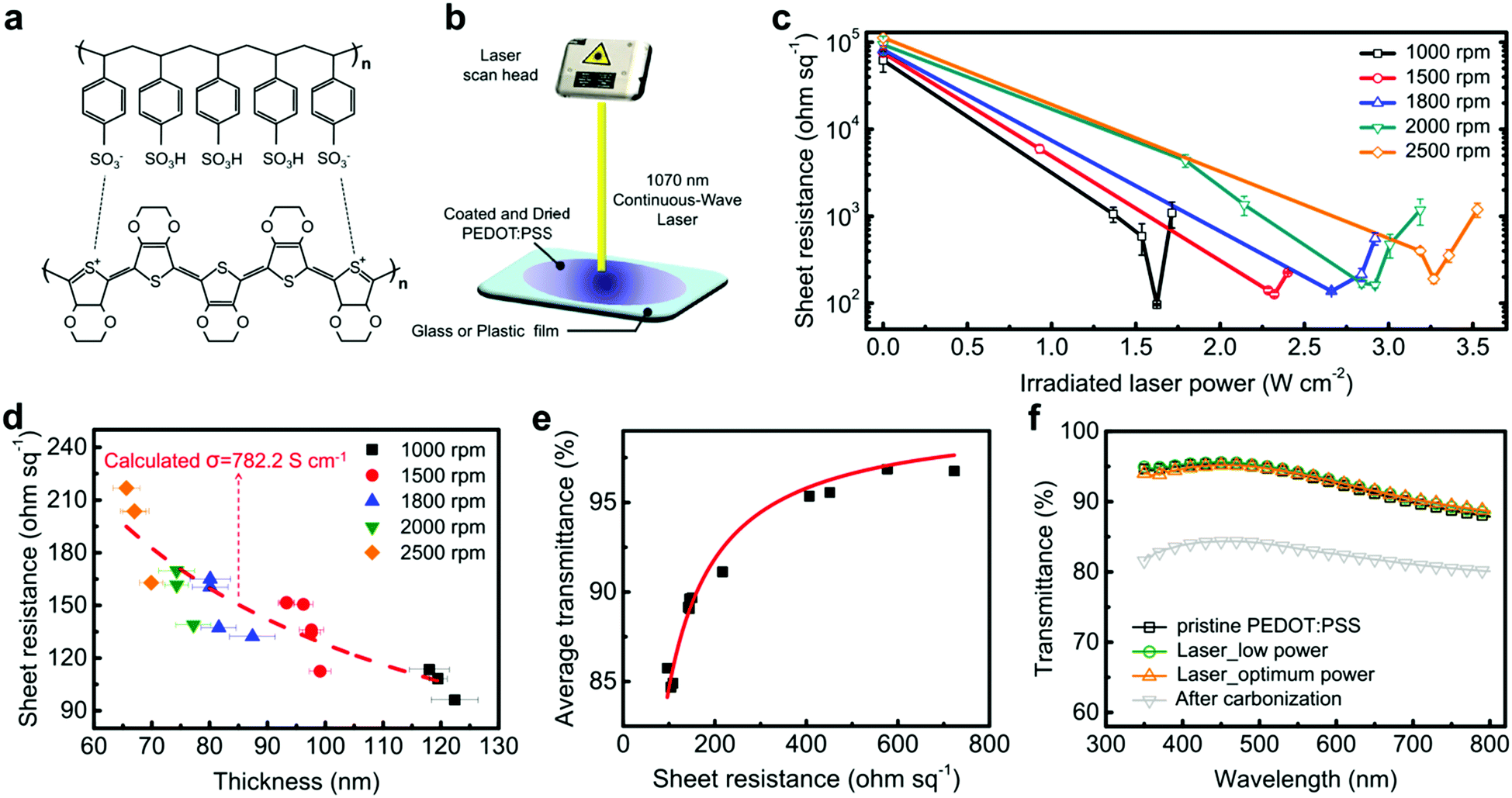 | ||
| Fig. 1 Chemical structure, electrical, and optical properties of PEDOT:PSS films. (a) Chemical structure of PEDOT:PSS. (b) Schematic of laser treatment of PEDOT:PSS films. (c) Sheet resistances for PEDOT:PSS films as a function of irradiated laser power and spin-speed. The error bars represent the standard deviation of several samples. (d) Optimized values of sheet resistances for laser-treated PEDOT:PSS films as a function of thickness. The error bars are determined from the standard deviation of film thickness. (e) Transmittances vs. sheet resistances of laser-treated PEDOT:PSS films. (f) Transmittance spectra of pristine PEDOT:PSS film and laser-treated PEDOT:PSS films prepared with different laser powers. | ||
However, the introduction of such solvents or acidic treatment to PEDOT:PSS is often undesirable for practical applications. Use of harsh acid such as H2SO4 can damage the integrity of polymeric substrates, thus preventing one from utilizing the mechanical flexibility, which is one of the most important benefits that organic electronics can offer. Even non-acidic solvent treatments could also lead to undesirable cases such as delamination of films and residual chemicals on the film surfaces (Fig. S1, ESI†), poor wetting properties on substrates, and inhomogeneous conductivity distribution in the film (Fig. S2 and S3, ESI†).
Here, we report a novel, solvent-free approach to increase the conductivity of PEDOT:PSS films using a laser. We show that laser illumination onto pristine PEDOT:PSS films can enhance their conductivity by three orders of magnitude, leading to conductivities as high as 932 S cm−1. Optical and chemical spectroscopy studies and microscopic electrical measurements reveal that the difference in photon absorption among PEDOT and PSS during laser treatment can lead to a selective structural reorganization of the insulative PSS nanoshells by which PEDOT subdomains are consolidated to form improved transport pathways and thus enhance the conductivity of PEDOT:PSS films. The proposed laser-based approach is highly beneficial in that it does not need any additional chemical substances including toxic acids and can be done in a more controlled manner by varying the laser intensity. Furthermore, the spatially selective irradiation of the laser beam can be used to define various conductivity patterns in PEDOT:PSS films in situ without resorting to photolithographic masks. To illustrate the key benefits and potentials of the proposed method, high performance organic photovoltaic cells and flexible transparent force touch sensors are demonstrated with the laser-treated PEDOT:PSS films.
2. Results and discussion
2.1. Laser generates electrical conductivity in PEDOT:PSS
The proposed laser-based approach is done by irradiating spin-coated pristine PEDOT:PSS films (conductivity of around 0.1 S cm−1) with an ytterbium fiber laser beam. The films are characterized as a function of spin-speed and irradiated laser power (Fig. 1c). The sheet resistances of pristine films prepared with different spin-speeds (1000–2500 rpm) range from 62k to 113k Ohm sq−1. The sheet resistances of the films rapidly drop by up to three orders of magnitude with laser treatment, showing different decrease rates with respect to the film thickness. The lowest sheet resistances for laser-treated PEDOT:PSS films range from 96.1 to 190.0 Ohm sq−1 where the optimum laser power varies with the thickness of the PEDOT:PSS films.We observe that thicker films need a lower laser power and vice versa. This implies that the degree of laser absorption depends on the thickness of the films. Above the optimum laser power, the sheet resistance increases, which might be due to partial damage, decomposition, or deformation of the polymer structures by laser-induced heat. The investigation of the photochemical degradation effects possibly occurring at high laser powers is required in future work. The calculated average conductivity of laser-treated PEDOT:PSS films with the optimum power is 782.2 S cm−1 (Fig. 1d). The conductivity is comparable to the high-conductivity PEDOT:PSS films using high-boiling point solvents dissolved in PEDOT:PSS solutions.13,14,19 The best performing laser-treated PEDOT:PSS film exhibits a conductivity of 931.9 S cm−1 (Table S1, ESI†). We next obtain the behaviour of sheet resistance and average transmittance (wavelength of 400–800 nm) of films. A minimum sheet resistance of 96.1 Ohm sq−1 is achieved for the films prepared with a spin-speed of 1000 rpm and a laser power of about 1.6 W cm−2, leading to an average transmittance of 85.7% (Fig. 1e). It should be noted that the laser-treated PEDOT:PSS films retain the original transmittance of the pristine films, excluding the possibility of carbonizing the films with an excessive laser power of 2.9 W cm−2 (Fig. 1f).
2.2. Identification of laser-induced conductivity
To understand the mechanism for the conductivity enhancement, we perform X-ray photoelectron spectroscopy (XPS) measurements on the pristine PEDOT:PSS and laser-irradiated PEDOT:PSS films with low (1.7 W cm−2), optimum (2.3 W cm−2), and high laser powers (2.7 W cm−2) (Fig. 2a). The XPS spectra show two strong S(2p) peaks, which correspond to the sulfonate groups of PSS at 167–172 eV and thiophene rings of PEDOT at 162–166 eV, respectively. The corresponding PEDOT peak increases with increasing laser power, indicating that laser treatment exposes PEDOT-rich domains at the surface of the film by a structural rearrangement of the PSS nanoshell. The reduction of PSS to PEDOT ratio might be caused by two reasons: (i) a reduction of PSS thickness surrounding PEDOT-rich domains; (ii) a reduction of the PSS quantity in the whole film. We conduct UV absorbance measurement to investigate the effect of laser treatment on the change of PSS amount in the bulk regime (Fig. 2b). The aromatic ring of PSS results in two strong absorption bands at a wavelength below 250 nm. Therefore, the most highly conductive PEDOT:PSS films enhanced by chemical post treatment show a strong reduction of PSS absorption peaks.16,17 It is interesting to note that our results do not show such a behaviour, indicating that the PSS quantity barely changes after laser treatment. In other words, the amount of PSS decreases at the surface of the films (XPS measurement) but does not change in the bulk of the films (UV absorbance measurement). These results imply that the PEDOT-rich cores emerge from the PSS matrix after laser treatment, but the total amount of PSS matrix is retained. Conductivities in PEDOT:PSS films of more than 1000 S cm−1 are generally obtained by solvent post treatment using EG, methanol, or H2SO4. These post-treated PEDOT:PSS films significantly reduce the PSS quantity, resulting in the improvement of conductivity with a great reduction of film thickness and decreased sheet resistance.13,16–18,20 However, our laser treatment preserves the film thickness and the quantity of PSS in the PEDOT:PSS films. The removal of surface PSS by laser treatment is also confirmed by contact angle measurements where the laser-treated PEDOT:PSS film is more hydrophobic compared to the pristine and EG-mixed PEDOT:PSS films due to the exposure of PEDOT-rich domains (Fig. S4, ESI†).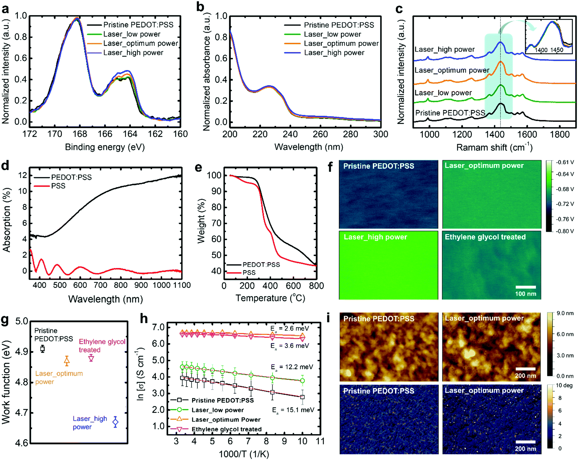 | ||
| Fig. 2 Chemical, optical, electrical, and structural characterization of PEDOT:PSS films. (a) XPS spectra for PEDOT:PSS films showing the change of PSS quantity at the surface of the films after laser treatment. (b) UV-absorbance spectra for PEDOT:PSS films illustrating no change of PSS quantity in the bulk of PEDOT:PSS films after laser treatment. (c) Raman spectra of PEDOT:PSS films showing no conformational change of PEDOT chains after laser treatment. The inset shows overlapped Raman bands. (d) Absorption spectra of PEDOT:PSS and PSS films, indicating that the 1.07 μm wavelength of the ytterbium laser beam is strongly absorbed by PEDOT while PSS does not absorb laser light. (e) Thermogravimetric analysis (TGA) for PEDOT:PSS and PSS films, showing that a thermal deformation of PEDOT:PSS is dominated by PSS. (f) The distribution of surface potential energy images for PEDOT:PSS films obtained by KPFM. (g) Work function of PEDOT:PSS films obtained from KPFM results. (h) Temperature dependence of the conductivity with Arrhenius fitting for PEDOT:PSS films. The error bars represent the standard deviation of several samples. (i) AFM topography (top) and phase images (bottom) for PEDOT:PSS films. All PEDOT:PSS films were prepared by spin-coating at 1500 rpm. | ||
As observed in earlier studies on highly conductive PEDOT:PSS films, chemical treatment for PEDOT:PSS films leads to a conformational change of PEDOT chains from benzoid to quinoid. The quinoid structure produces linear and expanded-coil conformations of PEDOT, which enhances charge conduction properties. The resonant structures of PEDOT can be confirmed by Raman spectroscopy measurements where the strongest band (1380–1470 cm−1) corresponds to the symmetric Cα![[double bond, length as m-dash]](https://www.rsc.org/images/entities/char_e001.gif) Cβ stretching modes of the aromatic rings in the PEDOT chains (Fig. 2c). The peak shift for the chemically treated PEDOT:PSS films has been widely reported,21–23 which is attributed to the conformational change of PEDOT chains as well as the enlarged PEDOT-rich cores by phase separation between PEDOT and PSS. Note that the laser-treated films do not show any peak shift in comparison with the pristine film. This indicates that laser treatment does not alter the conformation of the PEDOT chains. In other words, the degree of both coil and linear conformation of PEDOT chains is conserved after laser treatment. In addition, X-ray diffraction (XRD) measurements reveal that laser treatment preserves the crystallinity of PEDOT:PSS films (Fig. S5, ESI†). In contrast, chemical treatment considerably modifies the crystallinity of PEDOT chain packing as reported in the literature.17,19,24 These results suggest that laser treatment improves the charge transport properties in PEDOT:PSS films without causing significant phase separation of PSS and change of crystallinity in PEDOT-rich domains.
Cβ stretching modes of the aromatic rings in the PEDOT chains (Fig. 2c). The peak shift for the chemically treated PEDOT:PSS films has been widely reported,21–23 which is attributed to the conformational change of PEDOT chains as well as the enlarged PEDOT-rich cores by phase separation between PEDOT and PSS. Note that the laser-treated films do not show any peak shift in comparison with the pristine film. This indicates that laser treatment does not alter the conformation of the PEDOT chains. In other words, the degree of both coil and linear conformation of PEDOT chains is conserved after laser treatment. In addition, X-ray diffraction (XRD) measurements reveal that laser treatment preserves the crystallinity of PEDOT:PSS films (Fig. S5, ESI†). In contrast, chemical treatment considerably modifies the crystallinity of PEDOT chain packing as reported in the literature.17,19,24 These results suggest that laser treatment improves the charge transport properties in PEDOT:PSS films without causing significant phase separation of PSS and change of crystallinity in PEDOT-rich domains.
In pristine conditions, conductive PEDOT-rich cores are evenly buried in insulative PSS nanoshells. The wavelength of the light from the ytterbium fiber laser beam is 1.07 μm. In this spectral range, photons can be strongly absorbed by PEDOT, while it is not the case for PSS (Fig. 2d). Once these infrared photons are absorbed, PEDOT is expected to be heated up first. Subsequently, the generated intense heat energy in a PEDOT core is delivered most efficiently to the PSS shell that is in the closest proximity to that PEDOT core (Fig. 3). A macroscopic analogy may be found in the case where a wire carrying too much current melts away a cable jacket surrounding it by heat. As can be seen from the thermogravimetric analysis, the mass change of PEDOT:PSS at a high temperature is indeed dominated by thermal decomposition of PSS (Fig. 2e). That is, the PSS nanoshells are fragmented and undergo dynamic reorganization by the heat delivered from PEDOT in the intense and instant laser heating process; in this way, conductive PEDOT-rich cores even emerge from the region where the PSS shells originally exist, resulting in an enhanced contact between the conductive PEDOT-rich cores. These effects can reduce carrier hopping distances in between PEDOT-rich cores so that the electrical properties of PEDOT:PSS films are greatly enhanced. In this process, phase separation does not occur, as observed by XRD and Raman spectroscopy measurements.
 | ||
| Fig. 3 Schematic of the mechanism for conductivity-enhanced PEDOT:PSS by laser treatment. The laser irradiation results in the fragmentation of the PSS nanoshells, resulting in a favourable contact between the PEDOT-rich cores with effectively formed conducting pathways. | ||
We also perform heat treatment of PEDOT:PSS films using a hot plate, to check for a conductivity enhancement effect by thermal energy (Table S2, ESI†). However, no significant enhancement of the conductivity is observed because the thermal energy is simultaneously absorbed into both PEDOT and PSS. Therefore, it can be concluded that the significant heat-induced conductivity enhancement in PEDOT:PSS films can be realized dominantly by the laser heating method where the thermal energy is selectively absorbed in the PEDOT cores and subsequently transferred to the PSS shells enclosing them.
The amount of PSS has a direct impact on the surface potential energy of PEDOT:PSS films. The exposure of PEDOT area in the surface of the films is expected to increase by the proposed laser process. The fragmented PSS leads to the change in surface potentials of laser-treated films, as shown in the results of Kelvin probe force microscopy (KPFM) measurement shown in Fig. 2f. The laser-treated films do show an increase of surface potential due to a homogeneous reduction of the surface PSS. The corresponding work functions of laser-treated films decrease in comparison to that of the pristine film (4.91 eV) (Fig. 2g). The work function of high-conductivity films with optimum laser power is 4.87 eV, comparable to the 4.88 eV for the conventional EG-mixed PEDOT:PSS film. Higher laser powers further reduce the work function of the films, reaching a value of 4.67 eV. This can be understood by the fact that fragmented PSS barriers in laser-treated PEDOT:PSS films decrease the surface potential dipole of the films, resulting in an increase in the surface potential (i.e., decrease in work function) as reported in the literature.25,26 These observations support that the fragmentation of PSS barriers realizes a favourable contact between conductive PEDOT-rich cores, leading to an enhancement of conductivity. Fig. 2i exhibits atomic force microscopy (AFM) topography and phase images of the laser-treated and untreated PEDOT:PSS films. The surface structures of both films, which are indistinguishable, are commonly observed in PEDOT:PSS, providing evidence of a conserved phase for films after laser treatment. These results are consistent with the observations from scanning electron microscope (SEM) and SEM/energy dispersive X-ray spectroscopy (EDX) analysis (Fig. S6 and S7, ESI†), indicating that there is no significant change in the surface structure and chemical composition of PEDOT:PSS films after laser treatment.
The morphology of the conjugated polymers plays an important role in the charge conduction of the interconnected polymer domains. The enhanced electrical transport properties of laser-treated PEDOT:PSS films are further supported by measuring the temperature-dependent conductivity of the films (Fig. 2h). The laser-treated PEDOT:PSS films reveal a temperature-activated hopping behaviour typical for disordered conjugated polymer systems, following an Arrhenius law
 | (1) |
2.3. Selective in situ conductivity patterning
A notable feature inherent to the proposed laser treatment is the fact that one can vary the conductivity with spatial selectivity and irradiation controllability. This is not readily available with conventional methods. To demonstrate the gradual change of the conductivity enhancement during laser treatment, we irradiate a laser on the pristine PEDOT:PSS film connected to a light-emitting diode (LED) circuit (Fig. 4a and Movie S1, ESI†). With increasing laser-treated area, the LED glows brighter due to the gradual increase in the conductivity of the PEDOT:PSS film. As the conductivities can be tuned by adjusting the laser power, patterns with varying conductivities can be prepared. We demonstrate line patterns (5 × 140 mm2) with different conductivities on a large-area PEDOT:PSS film (200 × 200 mm2) by applying various laser powers (Fig. 4b and Movie S2, ESI†). Furthermore, we fabricate simple heating elements based on laser-patterned PEDOT:PSS films operated by the Joule heating effect. When applying a bias to the whole PEDOT:PSS film, the current mainly flows through the high-conductivity laser-defined area so that their local temperatures increase (Fig. 4c).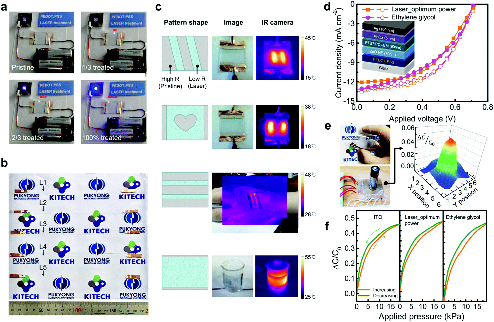 | ||
| Fig. 4 Patterning and device applications of laser-treated PEDOT:PSS films. (a) Photographs of the LED circuit in contact with the pristine PEDOT:PSS film. The LED becomes brighter during the laser irradiation process (Movie S1, ESI†). (b) Photograph of the laser-patterned PEDOT:PSS film on the large-area substrate (200 × 200 mm2). Five lines (indicated by arrows) are irradiated with various laser powers, showing different resistances (L1: 12 MΩ, L2: 990 kΩ, L3: 32 kΩ, L4: 11 kΩ, L5, 880 kΩ), when increasing the power of the laser from 0 to 3.57 W cm−2. This enables the selective doping effect in one substrate (Movie S2, ESI†). (c) Schematics, photographs, and infrared images of laser-treated PEDOT:PSS films with various patterns during Joule heating. (d) Current density–voltage curves of organic solar cells with the PEDOT:PSS films (filled symbols: ∼120 Ohm sq−1, open symbols: ∼90 Ohm sq−1). The inset is a schematic illustration of the device structure for organic photovoltaic cells. (e) Photographs of the FTFTS arrays based on the laser-treated PEDOT:PSS film (left) and capacitance map of FTFTS arrays with the laser-treated PEDOT:PSS film when a pressure object (a conventional AA-size battery) is loaded on the sensor (right). (f) Relative capacitance changes of FTFTSs in forward and reverse pressure-sweeps. | ||
The direct fabrication of different conductivity patterns demonstrates the wide applicability in optoelectronic array applications, e.g., as patterned transparent electrodes for printed organic solar cells, signage devices based on organic light-emitting diodes, or transparent electrical interconnections for flexible, stretchable electronic devices. Laser treatment can even be extended to flexible or stretchable polymer substrates (Fig. S3, ESI†), while conventional acidic solvent treatments cannot always be applied to these substrates. Moreover, solvent-mixed PEDOT:PSS films often result in poor wetting properties on substrates due to the high viscosity.24 For laser-treated PEDOT:PSS films, PEDOT:PSS solutions are coated on substrates in a pure state without solvents, exhibiting the excellent wettability on the various substrates while conventional EG-mixed PEDOT:PSS films suffer from poor film formation (Fig. S1–S3, ESI†).30–33 This enables the facile deposition of highly conductive PEDOT:PSS films on various substrates including hydrophobic substrates.
2.4. Optoelectronic devices with laser-patterned PEDOT:PSS
We fabricate high-performance inverted organic photovoltaic cells (OPV cells) by using the laser-treated PEDOT:PSS films as transparent electrodes. The current density (J)–voltage (V) characteristics of inverted bulk heterojunction OPV cells based on poly[[4,8-bis[(2-ethylhexyl)oxy]benzo[1,2-b:4,5-b′]dithiophene-2,6-diyl][3-fluoro-2-[(2-ethylhexyl)carbonyl]-thieno-[3,4-b]thiophenediyl]] (PTB7) and [6,6]-phenyl-C71-butyric acid methyl ester (PC70BM) are shown in Fig. 4d. The OPV cell with laser-treated PEDOT:PSS (∼90 Ohm sq−1) produces a short-circuit current density of 13.5 mA cm−2, an open-circuit voltage of 0.73 V and a fill factor of 0.50, exhibiting a power conversion efficiency (PCE) of 5.0%, whereas the control device based on the commonly available EG-mixed PEDOT:PSS film (∼90 Ohm sq−1) yields a short-circuit current density of 13.1 mA cm−2, an open-circuit voltage of 0.71 V and a fill factor of 0.53, yielding a PCE of 4.9%. The PCEs of the devices with the thinner, laser-treated and EG-mixed PEDOT:PSS films (∼120 Ohm sq−1) are 4.3 and 4.1%, respectively. Moreover, the OPV cells with the conventional architecture (PEDOT:PSS/active layer/LiF/Al) are fabricated using laser-treated and EG-mixed PEDOT:PSS films, and both devices show similar PCEs (Fig. S8, ESI†).The laser-treated PEDOT:PSS films can also be integrated into flexible transparent force touch sensor (FTFTS) arrays (Fig. 4e). The FTFTS is fabricated by sandwiching a clear acrylic elastomeric dielectric layer between a pair of TCEs including ITO, EG-mixed PEDOT:PSS, or laser-treated PEDOT:PSS on polyethylene terephthalate (PET) substrates. Fig. 4e shows the capacitance change map of the touch sensor arrays with the laser-treated PEDOT:PSS film in contact with an object (a commonly available 1.5 V-AA battery). It is clearly observed that the force is well concentrated around the object. Fig. 4f shows the capacitance change for single pressure touch sensors. The detectable pressures for all devices are about 1 kPa, enough to obtain sensory feedback in touch sensing. The touch sensor based on the laser-treated PEDOT:PSS film yields a similar capacitance change (sensitivity) compared to the sensor with the EG-mixed PEDOT:PSS film. These results of OPV cells and sensors imply that the highly conductive PEDOT:PSS films with laser treatment can achieve a device performance similar to the devices employing conventional EG-mixed PEDOT:PSS. The high conductivity together with solvent free, direct patterning capabilities of laser-induced PEDOT:PSS holds great promise for applications in various organic electronic devices.
3. Conclusions
In conclusion, we have discovered a new strategy to achieve high conductivity in PEDOT:PSS transparent films by laser irradiation, without the need for additional chemical substances. Laser treatment onto pristine PEDOT:PSS films significantly enhances the conductivity by three orders of magnitude, reaching a conductivity of up to ca. 932 S cm−1. This enhancement is achieved by the improved carrier transport properties due to a laser-induced reorganization of the PSS nanoshells with the help of component-selective laser absorption in PEDOT:PSS. The laser approach allows for facile conductivity patterning of the polymer films on large-area, flexible, stretchable substrates. Moreover, we have successfully demonstrated high performance organic optoelectronic devices including organic photovoltaic cells and flexible transparent force touch sensors with the proposed laser-treated PEDOT:PSS transparent conductive films. We believe that the proposed approach opens up a new avenue for the development of in situ patternable highly conductive polymers and their applications in various emerging electronics and optoelectronics.4. Experimental
4.1. Preparation of PEDOT:PSS films
PEDOT:PSS (Clevios PH1000) was obtained from Heraeus. PEDOT:PSS aqueous solution was filtered through a 0.45 μm syringe filter and spin-coated onto cleaned glass substrates, flexible PET substrates, and stretchable PDMS substrates which were pre-treated with oxygen plasma for more than 10 min. The PEDOT:PSS film on the large-area glass substrates with the size of 200 × 200 mm2 was prepared by the capillary coating system (BSE0004, BSP Inc.), where the gap between the capillary coater and the glass substrate was controlled at 150 μm. At a coating speed of 2.0 mm s−1, the thickness of the PEDOT:PSS film was about 70 nm. All the films were subsequently dried on a hot plate at 120 °C for 30 min. All the films were processed in ambient air.4.2. Laser treatment of PEDOT:PSS films
For the laser treatment process, we utilized a conventional single-mode continuous wave (CW) ytterbium fiber laser (YLR-20-Y11, IPG Photonics) with a lasing wavelength of 1.07 μm and a random polarization state. To perform the controlled and uniform irradiation of a laser onto the prepared PEDOT:PSS films, a laser scanning system (Cyclops-100, Beijing JCZ Technology, Co. Ltd) combined with the control software (EzCad2.1) was utilized in the laser-output. The size of the laser spot on the target was around 50–60 μm. To confirm the influence of laser power on the electrical properties of the PEDOT:PSS films, the scanning speed and the gap between the scanning lines were fixed as 2000 mm s−1 and 0.05 mm, respectively. This resulted in a scanning time of about 10 s for a sample area of 1 cm2. The irradiation power of the ytterbium laser was measured by using an optical power meter (PM200, ThorLabs) with an integrating sphere (S142C, ThorLabs). Some films were laser-patterned using a motion system for performing selective doping effects.4.3. Characterization of PEDOT:PSS films
Sheet resistance was measured by the van der Pauw method with a Keithley 2400 sourcemeter at room temperature. Optical transmittance and absorbance measurements were carried out using a UV-vis spectrophotometer (Optizen POP, MECASYS and Lambda 35, PerkinElmer). The film thickness was examined by a surface profilometer (KLA Tencor, P-16+), and confirmed by cross-sectional SEM views (Quanta3D FEG, FEI). The AFM topographic images were taken in tapping mode (Icon-PT, Bruker). The surface electronic states were analyzed by XPS (VG Multilab 2000, Thermo Electron Corporation) with an Al Kα X-ray source. Raman spectra were measured using a Renishaw spectrometer with a 532 nm Nd:YAG laser. The XRD patterns were recorded using a Rigaku D/MAX-2500 spectrometer. The temperature-dependent conductivity was obtained from current–voltage characteristics of PEDOT:PSS films at different temperatures (100–300 K) using the cryogenic probe station with liquid nitrogen. The films for AFM, XPS, Raman, XRD, and temperature-dependent conductivity analyses were prepared at a spin-speed of 1500 rpm.4.4. Measurements of work function
Changes of work function in the PEDOT:PSS films (1500 rpm) were investigated using an amplitude-modulated KPFM (Dimension Icon, Bruker Inc.). Work functions of samples (Wsample) can be correctly obtained by measuring contact potential difference (VCPD) with a known value of the work function of the tip (Wtip) because VCPD is defined as (Wtip − Wsample)/e where Wtip is the work function of the tip and e is the elementary charge (1.6 × 10⁻¹⁹ C). In our measurements, conventional conductive tips (EFM, Nanoworld) were used and the Wtip was calibrated with highly ordered pyrolytic graphite (HOPG) (work function of HOPG = 4.6 eV). The VCPD measurements were performed at 0.6 Hz of scan rate with 10 nm of distance between the tip and the samples. The represented work functions of the samples were calculated by averaged values in the images of VCPD (500 × 500 nm2) in a diagonal direction.4.5. Fabrication and characterization of PEDOT:PSS heaters
Pristine PEDOT:PSS solutions were spin-coated on the glass or PET substrates at a spin-speed of 1500 rpm and subsequently heated at 120 °C for 10 min. The fabricated PEDOT:PSS films were irradiated by a laser to obtain a high conductivity with the desired patterns. Both ends of the laser-treated PEDOT:PSS films were painted with a conductive paste and were wired to the power supply. A DC voltage was applied by a Keithley 2400 sourcemeter to obtain Joule heating for the laser-treated PEDOT:PSS films. The thermal images of the films were obtained using an infrared (IR) camera (TiS45, Fluke).4.6. OPV cell fabrication and evaluation
OPV cells were fabricated using 6 vol% EG-mixed PEDOT:PSS or laser-treated PEDOT:PSS transparent electrodes with the following structure: glass/transparent electrodes/ZnO nanoparticles (70 nm)/PTB7:PC70BM (90 nm)/MoOX (5 nm)/Ag (100 nm). A ZnO nanoparticle was spin-coated as an electron transport layer on top of PEDOT:PSS films at a spin speed of 4000 rpm and annealed at 100 °C for 10 min. The solution for ZnO nanoparticles was prepared according to the literature procedure.34 A blend of PTB7 and PC70BM as an active layer with a weight ratio of 1![[thin space (1/6-em)]](https://www.rsc.org/images/entities/char_2009.gif) :1.5 in chlorobenzene/1,8-diiodooctane (970 μl:30 μl) was spin-coated on top of the electron transport layer at a spin speed of 1000 rpm in an argon-filled glove box. After drying for 30 min at room temperature, MoOX and Ag were deposited on top of the active layer by thermal evaporation at a base pressure of 3 × 10⁻⁶ Torr. The current density–voltage (J–V) characteristics were measured using a solar simulator (PS-KS2C, MODUSYS) with a Keithley sourcemeter under AM 1.5G illumination with an irradiation intensity of 100 mW cm−2.
:1.5 in chlorobenzene/1,8-diiodooctane (970 μl:30 μl) was spin-coated on top of the electron transport layer at a spin speed of 1000 rpm in an argon-filled glove box. After drying for 30 min at room temperature, MoOX and Ag were deposited on top of the active layer by thermal evaporation at a base pressure of 3 × 10⁻⁶ Torr. The current density–voltage (J–V) characteristics were measured using a solar simulator (PS-KS2C, MODUSYS) with a Keithley sourcemeter under AM 1.5G illumination with an irradiation intensity of 100 mW cm−2.
4.7. Flexible transparent force touch sensor (FTFTS) fabrication and characterization
FTFTSs based on ITO or PEDOT:PSS transparent electrodes were fabricated by laminating two TCEs with the conducting path facing inward. A clear acrylic elastomeric adhesive (3MTM Scotch 924 ATG) with the base PET film was introduced as a dielectric layer of the prepared FTFTSs, where the overall dielectric spacer was 0.25 mm thick. The overlapping area between the TCEs was 2 × 2 mm2 for the single sensor and 10 × 10 mm2 for the FTFTS arrays. The capacitance values were collected using an impedance analyzer (Agilent, E4980A) and a pressure was applied using a lab-made pressure loading system with a pressure measuring unit (Nidec, FGJN-20). During the pressure-control experiment, a 1 mm-thick PDMS layer (Dow Corning, Sylgard 184) was placed between the pressure loading system and the FTFTS to make a uniform force distribution over the touching area.Conflicts of interest
There are no conflicts to declare.Acknowledgements
We thank J. Lee (Pukyong National University) for performing temperature-dependent conductivity measurements and J. Park (Korea Photonics Technology Institute) for setting up the laser system. This work was conducted with the support of the Korea Institute of Industrial Technology, as “Development of the flexible luminescence-battery sheet based on high oxygen/moisture barrier films for the luminescent smart packaging (KITECH JA-18-0040)”. This work was also supported by the Basic Science Research Program through the National Research Foundation of Korea (NRF) funded by the Ministry of Science, ICT & Future Planning (2016R1C1B2012490). D. C. Lim acknowledges support from the Korea Institute of Energy Technology Evaluation and Planning (KETEP, No. 20173030014180, 2018201010636A).References
- H. Shirakawa, E. J. Louis, A. G. MacDiarmid, C. K. Chiang and A. J. Heeger, J. Chem. Soc., Chem. Commun., 1977, 578–580 RSC.
- C. K. Chiang, C. R. Fincher, Y. W. Park, A. J. Heeger, H. Shirakawa, E. J. Louis, S. C. Gau and A. G. MacDiarmid, Phys. Rev. Lett., 1977, 39, 1098–1101 CrossRef CAS.
- G. MacDiarmid, Angew. Chem., Int. Ed., 2001, 40, 2581–2590 CrossRef PubMed.
- A. J. Heeger, Rev. Mod. Phys., 2001, 73, 681–700 CrossRef CAS.
- N. Basescu, Z.-X. Liu, D. Moses, A. J. Heeger, H. Naarmann and N. Theophilou, Nature, 1987, 327, 403–405 CrossRef CAS.
- J.-C. Chiang and A. G. MacDiarmid, Synth. Met., 1986, 13, 193–205 CrossRef CAS.
- B. Lüssem, M. Riede and K. Leo, Phys. Status Solidi, 2013, 210, 9–43 CrossRef.
- Y. H. Kim, J. Lee, S. Hofmann, M. C. Gather, L. Müller-Meskamp and K. Leo, Adv. Funct. Mater., 2013, 23, 3763–3769 CrossRef CAS.
- B. L. Groenendaal, F. Jonas, D. Freitag, H. Pielartzik and J. R. Reynolds, Adv. Mater., 2000, 7, 481–494 CrossRef.
- S. Kirchmeyer and K. Reuter, J. Mater. Chem., 2005, 15, 2077 RSC.
- K. Ellmer, Nat. Photonics, 2012, 6, 809–817 CrossRef CAS.
- C. J. M. Emmott, A. Urbina and J. Nelson, Sol. Energy Mater. Sol. Cells, 2012, 97, 14–21 CrossRef CAS.
- Y. H. Kim, C. Sachse, M. L. Machala, C. May, L. Müller-Meskamp and K. Leo, Adv. Funct. Mater., 2011, 21, 1076–1081 CrossRef CAS.
- H. Shi, C. Liu, Q. Jiang and J. Xu, Adv. Electron. Mater., 2015, 1, 1–16 Search PubMed.
- L. Ouyang, C. Musumeci, M. J. Jafari, T. Ederth and O. Inganäs, ACS Appl. Mater. Interfaces, 2015, 7, 19764–19773 CrossRef CAS PubMed.
- D. Alemu, H.-Y. Wei, K.-C. Ho and C.-W. Chu, Energy Environ. Sci., 2012, 5, 9662–9671 RSC.
- N. Kim, S. Kee, S. H. Lee, D. H. Lee, Y. H. Kahng, Y.-R. Jo, B.-J. Kim and K. Lee, Adv. Mater., 2014, 26, 2268–2272 CrossRef CAS PubMed.
- Y. Xia, K. Sun and J. Ouyang, Adv. Mater., 2012, 24, 2436–2440 CrossRef CAS PubMed.
- J. Rivnay, S. Inal, B. A. Collins, M. Sessolo, E. Stavrinidou, X. Strakosas, C. Tassone, D. M. Delongchamp and G. G. Malliaras, Nat. Commun., 2016, 7, 1–9 Search PubMed.
- M. Cai, Z. Ye, T. Xiao, R. Liu, Y. Chen, R. W. Mayer, R. Biswas, K.-M. Ho, R. Shinar and J. Shinar, Adv. Mater., 2012, 24, 4337–4342 CrossRef CAS PubMed.
- J. P. Thomas, L. Zhao, D. McGillivray and K. T. Leung, J. Mater. Chem. A, 2014, 2, 2383–2389 RSC.
- J. Ouyang, Q. Xu, C.-W. Chu, Y. Yang, G. Li and J. Shinar, Polymer, 2004, 45, 8443–8450 CrossRef CAS.
- B. Vaagensmith, K. M. Reza, M. D. N. Hasan, H. Elbohy, N. Adhikari, A. Dubey, N. Kantack, E. Gaml and Q. Qiao, ACS Appl. Mater. Interfaces, 2017, 9, 35861–35870 CrossRef CAS PubMed.
- F. Zabihi, Y. Xie, S. Gao and M. Eslamian, Appl. Surf. Sci., 2015, 338, 163–177 CrossRef CAS.
- T.-W. Lee and Y. Chung, Adv. Funct. Mater., 2008, 18, 2246–2252 CrossRef CAS.
- A. M. Nardes, M. Kemerink, M. Dekok, E. Vinken, K. Maturova and R. Janssen, Org. Electron., 2008, 9, 727–734 CrossRef CAS.
- N. I. Cracium, J. Wildeman and P. W. M. Blom, Phys. Rev. Lett., 2008, 100, 1–4 Search PubMed.
- V. Coropceanu, J. Cornil, D. A. da Silva Filho, Y. Olivier, R. Silbey and J. L. Brédas, Chem. Rev., 2007, 107, 926–952 CrossRef CAS PubMed.
- Y. Wang, C. Zhu, R. Pfattner, H. Yan, L. Jin, S. Chen, F. Molina-Lopez, F. Lissel, J. Liu and N. I. Rabiah, et al. , Sci. Adv., 2017, 3, e1602076 CrossRef PubMed.
- D. J. Lipomi, J. A. Lee, M. Vosgueritchian, B. C.-K. Tee, J. A. Bolander and Z. Bao, Chem. Mater., 2012, 24, 373–382 CrossRef CAS.
- M. Vosgueritchian, D. J. Lipomi and Z. Bao, Adv. Funct. Mater., 2012, 22, 421–428 CrossRef CAS.
- D. J. Lipomi, B. C.-K. Tee, M. Vosgueritchian and Z. Bao, Adv. Mater., 2011, 23, 1771–1775 CrossRef CAS PubMed.
- J. Y. Oh, M. Shin, J. B. Lee, J.-H. Ahn, H. K. Baik and U. Jeong, ACS Appl. Mater. Interfaces, 2014, 6, 6954–6961 CrossRef CAS PubMed.
- D. Liu and T. L. Kelly, Nat. Photonics, 2014, 8, 133–138 CrossRef CAS.
Footnote |
| † Electronic supplementary information (ESI) available. See DOI: 10.1039/c9mh00959k |
| This journal is © The Royal Society of Chemistry 2019 |