
 Open Access Article
 This Open Access Article is licensed under a Creative Commons Attribution-Non Commercial 3.0 Unported Licence
Ultrahigh hydrogen-sorbing palladium metallic-glass nanostructures†
Baran
Sarac
 *a,
Yurii P.
Ivanov
bc,
Tolga
Karazehir
d,
Marlene
Mühlbacher
e,
Baris
Kaynak
f,
A. Lindsay
Greer
b,
A. Sezai
Sarac
g and
Jürgen
Eckert
ae
*a,
Yurii P.
Ivanov
bc,
Tolga
Karazehir
d,
Marlene
Mühlbacher
e,
Baris
Kaynak
f,
A. Lindsay
Greer
b,
A. Sezai
Sarac
g and
Jürgen
Eckert
ae
aErich Schmid Institute of Materials Science, Austrian Academy of Sciences, 8700 Leoben, Austria. E-mail: baransarac@gmail.com
bDepartment of Materials Science & Metallurgy, University of Cambridge, Cambridge CB3 0FS, UK
cSchool of Natural Sciences, Far Eastern Federal University, 690950, Vladivostok, Russia
dDepartment of Energy System Engineering, Adana Arparslan Türkes Science and Technology University, 01250 Saricam, Adana, Turkey
eDepartment of Materials Science, Chair of Materials Physics, Montanuniversität Leoben, 8700 Leoben, Austria
fDepartment Polymer Science, Montanuniversität Leoben, 8700 Leoben, Austria
gPolymer Science and Engineering, Nanoscience & Nanoengineering, Istanbul Technical University, 34469 Istanbul, Turkey
First published on 23rd April 2019
Abstract
Pd-Based amorphous alloys can be used for hydrogen energy-related applications owing to their excellent sorption capacities. In this study, the sorption behaviour of dc magnetron-sputtered and chronoamperometrically-saturated Pd–Si–Cu metallic-glass (MG) nanofilms is investigated by means of aberration-corrected high-resolution transmission electron microscopy (HRTEM), X-ray photoelectron spectroscopy, and electrochemical techniques. The volume expansion of ΔV = 10.09 Å3 of a palladium hydride unit cell obtained from HRTEM images due to the hydrogenation of the Pd–MG nanofilms is 1.65 times larger than ΔV of the Pd-polycrystalline counterpart loaded under the same conditions. Determined by scanning transmission electron microscopy-high annular dark-field imaging and electron energy loss spectroscopy, the huge difference between the two Pd-based systems is accounted for by the “nanobubbles” originating from hydrogenation, which generate active sites for the formation and expansion of spatially dispersed palladium hydride nanocrystals. A remarkable difference in the hydrogen sorption capacity is measured by electrochemical impedance spectroscopy compared to the Pd polycrystal nanofilms particularly in the α and β regions, where the maximum hydrogen to palladium ratio obtained from a combination of chronoamperometry and cyclic voltammetry is 1.56 and 0.61 for the MG and Pd-polycrystal nanofilms, respectively. The findings place Pd–MGs among suitable material candidates for future energy systems.
New conceptsAdvanced materials with efficient hydrogen interactions are expected to play a major role in future energy conversion and storage systems. Despite their limited hydrogen storage capability and high costs, Pd-based nanomaterials are currently used for hydrogen storage and catalysis because of their excellent kinetic reversibility. Among them, Pd-based metallic glasses (Pd–MGs) can be considered as more efficient candidates due to their grain-free amorphous nanostructure with extra interstitial sites for a higher amount of hydrogen sorption. This study comprises, for the first time, an in-depth study of the unique hydrogenation behaviour of Pd–MG nanofilms sputtered on a Si substrate via physical vapour deposition. Aberration-corrected HRTEM and STEM-HAADF/-EELS techniques confirmed the lattice expansion of 10.09 Å3 obtained from the FFT patterns, which corroborates the extensive sorption capacity of Pd-based MGs (around 1.65 times larger than that for its Pd-counterparts). Compared to the lattice expansion of the Pd polycrystal nanofilms with the same thickness (50 nm), the calculated maximum H/M = 1.56 is 2.55 times larger. The considered Pd–MG improves the overall hydrogen storage capability through the electrochemically-induced nanobubbles. The ground-breaking concept of this study is that we have remarkably enhanced the metal–hydrogen interaction and palladium hydride formation via a newly designed nanofilm (Pd79Si16Cu5) and electrochemical hydrogenation. |
As an abundant, clean and renewable energy source, hydrogen is evaluated as a new material for the replacement of the currently used fossil fuels. Compared to other hydrogen storage techniques,1–3 metal hydrides have the capability of storing large amounts of hydrogen without the need for external pressure or heat.4–6 Due to the absorption of hydrogen into the bulk layers of the metal,7–9 current state-of-the-art metal hydrides have higher volumetric density and lower total storage energy (12.5% of the net calorific value of hydrogen10) as compared to the hydrogen gas or liquid hydrogen. Moreover, compared to physisorption, metal hydride formation via electrochemical bonding is generally accepted to yield higher volumetric and gravimetric densities of hydrogen storage.11
Palladium is one of the key materials currently used for hydrogen storage and catalysis with excellent kinetic reversibility at ambient temperatures.12–14 However, the high cost of Pd in bulk and micro-scale size and its moderate affinity to oxidizing or reducing environments under extreme conditions create big barriers against energy-based industrial applications.12,15 Cu containing PdSi-based metallic-glass (MG) nanofilms can serve as a remedy to this problem by showing higher durability against severe environments due to their grain-free amorphous structure while significantly decreasing the cost due to the substitution of Pd with Si and Cu.16 In our previous study, the electrosorption (adsorption, absorption, desorption, and evolution) behaviour of hydrogen and kinetic parameters such as charge transfer resistance, as well as the double layer and adsorption capacitance were investigated using a combination of cyclic voltammetry and electroimpedance spectroscopy.17 Depending on the Cu content, PdSi-based metallic glass nanofilms can remarkably enhance metal–hydrogen interaction and palladium hydride (PdHx) formation. Although this phenomenon can be linked to the non-translational structural motifs on the nm scale and the free volume in Pd-based metallic glasses, which probably generates additional interstitial sites for a higher amount of hydrogen sorption,18–20 the mechanism and extent of palladium hydride formation in these multicomponent amorphous nanofilms are still unclear.
Here, we utilized an aberration-corrected high-resolution transmission electron microscopy (HRTEM) technique with a point-to-point resolution of less than 0.1 nm, which allows characterization of palladium hydride crystals with diameters of several nanometers. Composition and thickness analyses were performed by high-angle annular dark-field imaging in scanning transmission electron microscopy mode (HAADF-STEM) in order to assess the chemical segregation within the Pd–Si–Cu nanofilm due to electrochemical hydrogenation. A comparative study with unhydrogenated Pd–Si–Cu nanofilms, as well as a polycrystalline Pd nanofilm of similar thickness, was performed to highlight the extent of hydride formation in each case. The hydrides accumulate around “nanobubbles” with diameters of up to 4 nm, which is discovered to be the main reason for the ultra-high amounts of hydrogen storage in PdSiCu metallic-glass nanofilms.
A typical dc magnetron-sputtered nanofilm on a silicon chip is shown in Fig. 1a. Grazing incidence X-ray diffraction (GIXRD) analysis shows a broad diffraction maximum for the Pd79Si16Cu5 nanofilm (Fig. 1b) as opposed to the sharp peaks obtained for the polycrystalline Pd nanofilm (Fig. S1a – ESI†). The first peak maximum of the Pd polycrystal (40.12°) shifts to a larger 2θ value for the MG sample (40.54°) by the inclusion of Si and Cu. Similar to the literature findings, upon Cu addition, our previous XRD investigation showed a remarkable decrease in the interatomic lattice spacing (i.e. volumetric contraction) due to the smaller atomic radii of Cu. This results in broadening of the first sharp peak of the Pd sample, where this peak is strongly influenced by the contributions of Pd–Si and Pd–Cu bonds.17 The first diffuse peak maximum of Pd84Si16 (2θ = 40.28°) shifts to 2θ = 40.54° for the 5 at% Cu addition (Pd79Si16Cu5). The more Pd is replaced with Cu, the bigger the shift in 2θ towards larger values.
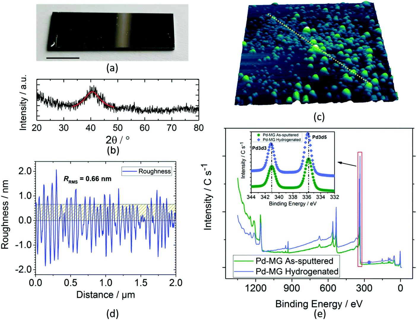 | ||
| Fig. 1 Synthesis and structural/surface characterization of a Pd79Si16Cu5 film. (a) Digital microscopy image of a PVD sputtered film on a Si substrate with coating dimensions of 1.8 mm × 0.6 mm (scale bar 1 mm). (b) GIXRD analysis of the same film. Fitting of the first broad peak using the pseudo-Voigt function. (c) 3D profile analysis of a 2 × 2 μm region of a MG thin film performed via AFM. (d) Line scan (yellow dashed lines in c) of the AFM image; the root mean square roughness is 0.66 nm. The line-scan roughness for the Pd polycrystalline sample is 0.29 nm. (e) Survey scan of the Pd–MG as-sputtered (unhydrogenated) and hydrogenated samples. The magnified view of the red area shows the Pd 3d3 and Pd 3d5 valence states. The black dashed lines pass through the maxima points of the two valence states of the as-sputtered sample. A slight shift in the maxima of the hydrogenated sample towards higher binding energies is observed (∼0.2 eV). | ||
The line scan profile obtained by atomic force microscopy (AFM) analysis in Fig. 1c shows a surface roughness of RRMS = 0.66 nm (Fig. 1d). The root mean square roughness, RRMS, obtained from the scanned area is 0.64 and 3.37 nm for the Pd and MG thin films, respectively. PdSi-based metallic glasses with Cu content were found to have higher surface roughness compared to the PdSi–MGs without Cu. On the other hand, our previous findings obtained from the electrochemical circuit modeling (ECM) show that hydrogen absorption in Pd-based glassy thin films is mainly independent of this roughness factor.17 Compared to the inhomogenously scattered bumps obtained from the 3D profile of PdTF as shown in Fig. S1b (ESI†), the MG shows a more homogenous dispersion of surface asperities. For the Palladium Thin Film (PdTF) and Metallic-Glass Thin Film (MGTF) samples, the correlated actual surface areas obtained from the AFM measurements for the 4 μm2 projected area are 4.005 μm2 and 4.077 μm2, respectively. For the cyclic voltammetry of samples with such small roughness values, the literature theoretically and experimentally proves the independence of the electrode roughness in relation to the shape of the CV curves and peak currents.21
The X-ray Photoelectron Spectroscopy (XPS) study survey scan (Fig. 1e) shows a small shift in the peak maxima of Pd 3d3/2 and Pd 3d5/2 valence states towards higher binding energies (inset) upon electrochemical hydrogenation. Si 2p3, Cu 2p1/2, and Cu 2p3/2 peaks do not shift after hydrogenation (as confirmed in our previous work).17 Thus, no chemical interaction between Si and H, and Cu and H has been detected after hydrogenation. For this reason, Pd is the main metal interacting with the sorbed hydrogen from the active sites of the MG sample. Fig. S2 (ESI†) shows the seamless attachment on the atomic-scale between the Si/SiO2 substrate and the MG nanofilm before hydrogenation. Fig. S3 (ESI†) shows an HRTEM image of a hydrogenated Pd thin film. It reveals the polycrystalline structure of Pd with an average grain size of 10–20 nm. The thickness of the polycrystalline layer was measured to be ∼40 nm. Due to the high precision and stability of the employed PVD sputtering technique, the thickness of the polycrystalline layer is constant across the sample.
To evaluate the saturation time and to determine the sorbed hydrogen in terms of the applied potential, we have performed combinatorial chronoamperometry (Fig. S4 – ESI†) and cyclic voltammetry (Fig. S5 – ESI†) tests using the MG sample. At higher saturation potentials (from 0.4 V to 0.2 V vs. RHE) the sample readily reaches its hydrogen saturation limit within 10 seconds. In comparison, ∼50 μm Pd foil in 1 M H2SO4 solution can be saturated in ca. 300 s.22 Such fast hydrogenation kinetics of this film is mainly due to its considerably small thickness of 50 nm. While the hydrogen evolution reaction starts below 0.15 V (inset), MG cannot fully store readily sorbed hydrogen. The release of excess hydrogen leads to an increase in the current density.
After chronoamperometric saturation, cyclic voltammograms of the nanofilms were recorded. Fig. 2a shows the cathodic (navy blue) and anodic (green) scans of the Pd–MG nanofilm saturated at 0.2 V. The changes in the shapes of the scans in the charge transfer resistance, RCT, obtained from the equivalent circuit model of the EIS data were ascribed to phase transformations (see Fig. S6 – ESI†). A double-layer region is observed above 0.28 V, corresponding mainly to the formation of a solid-solution in the metal (the α phase). Between 0.28 V and 0.18 V, electrochemically-bonded hydrogen starts to diffuse into the bulk sample while more hydrogen attaches to the surface (the α + β phase). As the potential drops down, between 0.18 V and 0.04 V, absorption dominates due to the transfer of hydrogen ions into the bulk sample and their attachment to the active sites (the β phase). On the contrary, the desorption of hydrogen from these sites and the movement of hydrogen towards the surface is observed in the anodic scan within the same region. With the sharp decrease in the current density, the electrocatalysis of hydrogen starts to take place below 0.04 V in the cathodic scan.
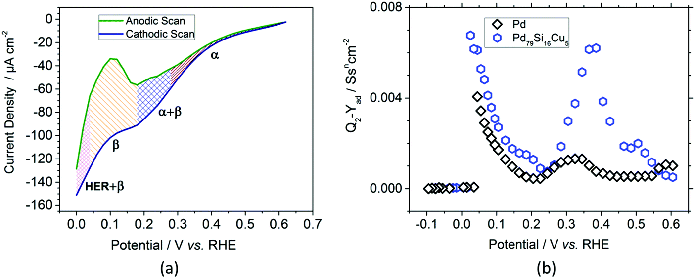 | ||
| Fig. 2 Electrochemical measurements of the nanofilms. (a) Current density as a function of potential, obtained from cyclic voltammetry for Pd79Si16Cu5 MG. The hatched regions are depicted by α = wine, α + β = blue, β = orange, and HER + β = magenta. (b) Hydrogen adsorption capacitance parameter (Q2 − Yad) vs. potential of the Pd crystal and Pd79Si16Cu5 MG obtained by the equivalent circuit modelling of the electrochemical impedance spectroscopy (EIS) data. | ||
The ECM was further employed to model the impedance spectra of the MG and crystalline Pd nanofilms to investigate their capacitive response. In our previous study, the replacement of Pd with Cu by only 5% was proven to have a tremendous increase in the double layer and adsorption capacitance of the PdSi-based MG thin films.17 The adsorption capacitance parameter, Yad, calculated from the impedance values of the constant phase element (details given in the ESI† – Materials and methods, Electrochemical measurements) is shown in Fig. 2b. In the double-layer region, the maximum of the Pd79Si16Cu5 MG nanofilm is 4.7 times larger than that of the Pd crystal. Similarly, in the underpotential deposition (UPD) region, the maximum recorded value of the MG nanofilm is 1.67 times larger than that of the Pd crystal. However, in the over potential deposition (OPD) region, a sharp decrease in Yad below 0.025 V is observed as the hydrogen evolution reaction (HER) starts to dominate. The high homogeneity also resulted in the increase of the adsorption capacitance parameter Yad, as confirmed in our previous work.17 The results clearly highlight the fact that compared to conventionally used polycrystalline Pd, for a similar thickness (52.5 nm) and surface area the selected MG type exhibits a larger amount of hydrogen adsorption and absorption capacity.
A schematic of the hydrogenation mechanism is shown in Fig. 3a. The adsorbed hydrogen ions on the surface penetrate into bulk Pd,23 in turn reaching the Si substrate which acts as a barrier. The accumulation of the hydrogen ions at the interface leads to the formation of palladium hydride crystals (indicated by yellow and gray atoms). The increase of the hydrogenation in palladium hydride crystals generates an outward pressure leading to nanobubble formation. The excess H+ ions diffuse out directly or through small chimneys, and depending on the applied potential, might subsequently leave the surface through reduction in the form of hydrogen gas.24 Aberration-corrected high-resolution transmission electron microscopy was used to investigate the reasons behind the dramatic changes in the Pd–MG nanofilms upon hydrogenation. Fig. 3c and d show the spatially dispersed nanobubble formation along the nanofilm. Fig. S7a (ESI†) is an enlarged image of these nanobubbles taken by HRSTEM. HRTEM images taken from 3 different regions (Fig. 3b and Fig. S7b – ESI†) show a clear contrast between the bubbles and the MG matrix. Fig. 3c shows a bright-field TEM image of the Si–MG assembly. Bubble-shaped structures emanating from the substrate surface expand and generate nanobumps on the nanofilm surface. The HAADF-STEM images in Fig. 3d display the nanobubbles forming on the Si substrate. The matrix around the bubbles is slightly darker than the other regions indicating that the MG is pushed outwards due to hydrogenation. Although no clear nanosegregation was observed in the MG matrix, Si depletion of around 4% in the very surrounding of the nanobubbles was determined from the image analyses of the EELS data. Thin nanohumps were formed on the top surface of the MG due to the outward pressure of the accumulated hydrogen at the interface.
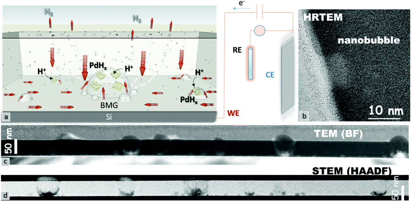 | ||
| Fig. 3 Palladium hydride formation around the nanobubbles by means of chronoamperometric saturation is schematically described in (a). Visualization of nanobubbles in the MG nanofilms via (b) HRTEM, (c) low magnification BFTEM and (d) STEM-HAADF. A Pt layer of ∼50 nm behind the nanobumps is coated on the MG film for the TEM sample preparation by FIB. | ||
Fig. S8a (ESI†) shows a HAADF-STEM image of electrochemically hydrogenated polycrystalline Pd. Fig. S8b (ESI†) shows the elemental mapping of Pd, Si and the interlayer SiO2. The Pd content is uniform across the sample, which was confirmed by EELS mapping. From the micrographs, no palladium hydride can be detected at the interface between the Si substrate and the crystalline Pd nanofilm. This result confirms that the nanobubble formation is unique to Pd79Si16Cu5 nanofilms. The thickness map of the MG nanofilm in Fig. S9a (ESI†) shows that the relative specimen thickness t/λ (thickness expressed in units of the inelastic mean free path) decreases severely (from 0.7 to 0.6 t/λ) during nanobubble formation. On the other hand, the strong decrease in thickness as shown in Fig. S9b (ESI†) is mainly due to the contribution of diffraction scattering from the polycrystalline structure of Pd.
The HRTEM micrograph of a Pd–MG nanofilm provided in Fig. 4a reveals the structural differences between the unhydrogenated regions (Fig. 4c(1)) and the hydrogenated regions in the vicinity of the nanobubbles (Fig. 4c(2)). The composition analysis of all the investigated and individual elements performed by EELS is depicted in Fig. 4b. Region 1 constitutes a maze-like structure with a broad diffuse halo on the fast Fourier transform (FFT) pattern of the HRTEM image (Fig. 4d(1)). On the other hand, palladium hydride crystals are observed on the top or back layer of the nanobubbles, where point maxima on the broad diffuse FFT pattern can be seen in Fig. 4d(2). The superimposed FFT pattern of the first and second regions (Fig. 4d) shows that the two main lattice fringes found in the FFT pattern from the region close to the nanobubble correspond to fcc-Pd and fcc-PdHx nanocrystals with (111) (0.225 nm and 0.2286 nm, inside rings) and (200) (0.194 nm and 0.198 nm, outside rings) planes, respectively. The magnified image of a nanobubble as shown in Fig. 4e reveals that the diameters of the nanocrystals range from 1 to 4 nm, confirming the formation of extremely small crystals around the hydrided regions.
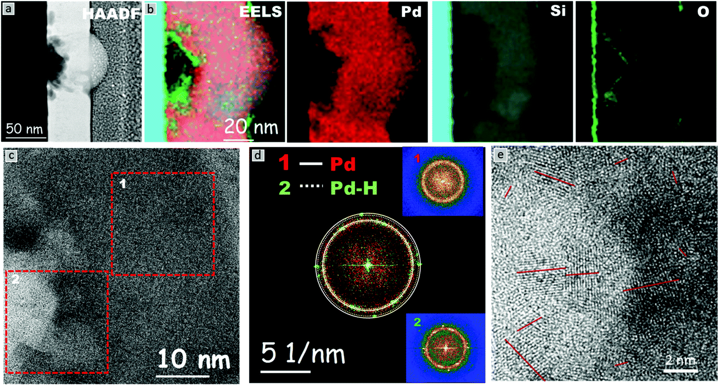 | ||
| Fig. 4 High-resolution chemical composition study of the Pd–MG nanofilm. (a) HAADF-STEM and (b) EELS analysis of the assembly. Pink color indicates the high abundance of Pd with relatively lower Si, where traces of oxygen obtained from the SiO2 layer are observed. Individual Pd (red), O (green) and Si (blue) compositions within the Pd–MG nanofilm are shown. Due to the origin of the dark-field image, a minimum amount of signal can be attained from the porous regions (observed in black). Structural evaluation of the hydrogenated MG nanofilm. (c) Recorded HRTEM images obtained from the (1) unhydrogenated amorphous and (2) nanobubble containing palladium hydride nanocrystals. (d) Corresponding superimposed FFT patterns exhibiting a broad diffuse halo for (1), and point maxima on the broad halo for (2) (separated FFTs are given in the insets). The continuous and dashed lines correspond to the lattice fringes of the fcc Pd and Pd–H nanocrystals, respectively. The outer and inner rings represent the (200) and (111) planes, respectively. (e) Magnified view of the hydride regions with nanocrystals of diameters ranging from 1 to 4 nm. | ||
The HRTEM and HAADF-STEM micrographs reveal that the majority of the large bubbles initiate from the Si–MG interface. This is mainly because the hydrogen ions, dissociated from the diluted sulfuric acid solution via the applied potential, propagate towards the inner layers until reaching the Si substrate which acts as a barrier. Several nanometers of SiO2 layer on the substrate mediates the H+ entrapment due to the partial negative charge of oxygen and results in Si–O⋯H formation.25 The entrapped hydrogen ions subsequently give electrons to palladium, which leads to PdHx formation. The increase in the hydrogen content as a function of the applied voltage in turn forms an inner diaphragm and a nanobump on the MG surface. Smaller bubbles generated from the big bubble and from the interface, as well as hydrogen pathways towards the top surface of the nanofilm, are observed. The kinetic energy of the hydrogen ions can be further accelerated by optimizing the applied potential and time of hydrogenation, which would in turn influence the diameter and number of nanobubbles. The maximum solubility of hydrogen in the β-phase is ∼35 times larger than that in the α-phase. The diffusion coefficient of hydrogen in the β-phase is ∼3.33 times larger than that for the α-phase (ratios calculated from ref. 22). Furthermore, our chronoamperometry and CV studies have shown that (de)hydrogenation occurs in a matter of seconds. Hence, the adopted Si–MG assembly can partially be charged and discharged by hydrogen at fast rates and without the need of generating new nanobubbles. From this study, it is deduced that the Si/SiO2 substrate plays a key role in heterogenous nucleation of PdHx crystals from the surface. Besides the Si/SiO2 and MG interface, artificial interfaces such as pores or second phases can be introduced from which the nanobubbles could nucleate via palladium hydride formation. On the other hand, polycrystalline Pd nanofilms produced by using the same PVD method do not exhibit such nanobubble formation even after reaching the hydrogen saturation limit via chronoamperometry. This confirms that hydrogen cannot effectively penetrate into the bulk layers of the Pd polycrystal nanofilm. Another problem is that the hydrogen atoms can reside only at the interstitial sites of the polycrystalline Pd, which limits the amount of hydrogen turning into the hydride form.
Fig. S10a–c (ESI†) shows the SAED patterns taken from the superposition of the diffraction of the hydrogenated Pd nanofilm (Fig. S10a, ESI†), the individual Si substrate (Fig. S10b, ESI†) and the Pt layer (Fig. S10c, ESI†). Hereafter we analyzed the HRTEM images taken from the Pd nanofilm (Fig. S10d and f, ESI†) and the HRTEM image of the Pt layer as a reference (Fig. S10e, ESI†). Fig. S10g (ESI†) shows the azimuthal profile of the FFT patterns taken separately from the Pt layer and the hydrogenated Pd film. The shift of the peak positions of the hydrogenated Pd film towards smaller reciprocal values (larger real space values) is clearly visible. Both peaks correspond to the (111) and (200) planes of an fcc structure. The average lattice constants for the Pt layer and the hydrogenated Pd film are measured as 0.392 ± 0.002 nm and 0.402 ± 0.002 nm, respectively. The lattice constant of the hydrogenated polycrystalline Pd film has the same value as previously reported.26 Thus, the value for the hydrogenated Pd film is 0.402 ± 0.002 nm, which is much larger than the original Pd (fcc) lattice constant of afcc_Pd = 0.389 ± 0.002 nm as confirmed by the literature.26,27
In contrast to the crystalline Pd film the amount of lattice expansion in MG films is more difficult to estimate due to the lack of long range order in metallic glasses. Fig. S11a and c (ESI†) show additional HRTEM images of the MG nanofilms after hydrogenation. It is clearly seen that from the FFT patterns in Fig. S11b and d (ESI†) the appearance of the diffraction spots superimposed on the diffuse ring from the amorphous matrix. These spots correspond to the formation of the palladium hydride nanocrystals at the nanobubble locations. The contribution of Pd hydride formed within the amorphous MG matrix is marked also by the red dashed line on the azimuthal profile of the FFT pattern shown in Fig. S11e (ESI†) which corresponds to 0.232 ± 0.002 nm of (111) PdHx, and a calculated lattice parameter of 0.402 ± 0.002 nm. Moreover, Fig. S11e (ESI†) shows that the peak position of the broad maximum obtained from the MG matrix shifts to 0.225 ± 0.002 nm in comparison to the as-sputtered sample at 0.220 ± 0.001 nm obtained from the maximum of the first diffuse peak (20.54° determined from the pseudo-Voigt fit of the XRD diffractogram as shown in Fig. 1b). Thus, although we cannot directly compare the difference in the lattice expansions of the MG and polycrystalline Pd films, from the measured average atomic distances of the initial MG film we calculate the fcc lattice parameter of the very first Pd hydride crystals formed within the MG matrix as 0.380 nm. This value is lower than that of the initial polycrystalline Pd nanofilms of 0.389 nm. Upon hydrogen saturation the lattice parameter of the crystalline PdHx phase reaches the same lattice constant of 0.402 nm. Since the volumetric expansion difference is on the third power, a huge volumetric expansion is observed for the MG films, which can be assigned to the abundance of free volume acting as the active sites for the hydrogen entrapment. The average volumetric expansion, V = VPdHx − VPd, for Pd and Pd79Si16Cu5 nanofilms is calculated as 6.10 Å3 and 10.09 Å3, respectively. These results indicate that the lattice expansion of selected MG after hydrogen saturation is higher than any Pd alloys under ambient conditions.28 In fact, hydrogen in β palladium hydride is commonly accepted to be by octahedral interstitial site occupation of an fcc unit cell, which leads to a theoretical limiting H to Pd ratio of 1 (H/M = 0.7).7,29 Thus, the amount of hydrogen entrapment is much less, which is not sufficient to generate nanobubbles. On the other hand, for the Pd–Si–Cu MG system, Pd-centered trigonal prisms capped with Cu atoms, as obtained from neutron diffraction experiments and molecular dynamics simulations, might result in the generation of more sites that are active for hydrogen entrapment.19,20,30,31 Moreover, due to the abundance of free volume between the atomic clusters as seen in atomic simulations,32,33 the hydrogen ions can easily pass through the amorphous matrix and accumulate at the interface. The loosely packed structure with randomly dispersed interstitial holes in the supercooled liquid phase and its sluggish crystallization kinetics are the main reasons for the high abundance of such active sites.34,35 Thus, a higher entrapment of hydrogen in ion form can be attained, leading to the unit cell expansion of the formed PdHx crystals.
H/M ratio vs. applied potential graphs in Fig. S12 (ESI†) clearly show that the rate of hydrogenation increases below 0.15 V for both samples. The H/M ratio for the Pd nanofilm already starts with 0.62 after the chronoamperometric saturation for 850 s at 0.6 V. This clearly means that MG can readily sorb similar amounts of hydrogen to the maximum saturation limit of hydrogen in Pd. The maximum H/M ratios observed for the considered range are 0.61 and 1.56 for the Pd and MG nanofilms, respectively. Thus, around 2.5 times higher hydrogen sorption is possible with the MG nanofilm. The increase in H/M values and the trend of increase towards smaller potentials are in line with the previous finding conducted in an acidic environment with Pd nanoparticles.36 The corresponding maximum weight percent of hydrogen (max. wt% H) for the Pd and MG nanofilms is 0.57 and 1.48%, respectively. This finding correlates well with literature values of H/M and max. wt% H of pristine Pd,2,37–40 where small differences can be due to the electrolyte concentration/type, as well as the Si substrate used in this study. The hydrogen storage capacity of the selected MG nanofilms is comparable to many other conventionally used materials such as Mg2Ni, Ti, V, Zr, LaNi5, FeTi, Cu–Ni, TiFe, TiS2 and even the newly discovered high entropy alloys.2,28,41–44 As confirmed by the HRTEM, the hydrogenation is more favored in the heterogenous nucleation sites. Thus, further control or design of such interfaces might enhance the amount of stored hydrogen.
Table S1 (ESI†) summarizes hydrogen sorption of different materials such as Mg-rich powders, complex light-metal hydrides, carbon nanotubes, zeolites, metal organic frameworks, hydride slurries, aerogels, liquid/compressed hydrogen, high entropy alloys, and metallic glasses in terms of maximum weight percent of stored hydrogen (wt% of H) and the atomic ratio of hydrogen to metal (H/M). Compared to many other metal-hydride formers, Pd exhibits long-term cycling stability up to 2500 cycles,45 and excellent kinetic hydrogen reversibility due to a very low enthalpy of formation of hydride in Pd.41,46 In terms of electrocatalytic activity of the selected MG film, our recent findings obtained from the Tafel plots exhibit a slightly smaller Tafel slope and higher exchange current density, revealing that the H2 evolution kinetics is faster than that of the Pd nanofilms.
Conclusions
In this contribution, we assessed the electrosorption capacity of hydrogen in PVD-sputtered Pd79Si16Cu5 MG nanofilms of ∼50 nm thickness comparatively with Pd polycrystalline specimens. Palladium hydride in the amorphous nanofilm is formed in the vicinity of nanobubbles, which originates from its interface with the Si substrate. HRTEM images corroborate the presence of crystals, 1 to 4 nm in diameter, spatially dispersed around the nanobubbles. From the corresponding FFT pattern comparison acquired from the hydride regions and the fully amorphous matrix, a volume expansion of 10.09 Å3 is found. On the other hand, for hydrogenated polycrystalline Pd, the volume expansion is only 6.10 Å3, which is in agreement with previous findings. The calculated ratio of H/M = 1.56 of the Pd79Si16Cu5 MG nanofilms obtained from the electrochemical hydrogenation, which is around 2.5 times larger than that of the Pd nanofilms, places them among promising materials for future energy systems.Conflicts of interest
The authors declare no financial interest.Acknowledgements
The authors commemorate Dipl-Ing Dr Mont. T. Schöberl, who was involved in performing the AFM study and who tragically lost his life in a traffic accident. The authors thank P. Zefferer for technical support, C. Mitterer and B. Putz for providing the sputtering device for synthesizing the MG and Pd nanofilms, and S. Ketov, and C. Gammer for fruitful discussions. The authors thank Prof. Andrey Chuvilin from CIC NanoGUNE, Spain, for technical support of TEM experiments and fruitful discussions. This work was supported by the European Research Council under the Advanced Grants “INTELHYB – Next generation of complex metallic materials in intelligent hybrid structures” (Grant ERC-2013-ADG-340025) and “ExtendGlass – Extending the range of the glassy state: Exploring structure and property limits in metallic glasses” (Grant ERC-2015-ADG-695487). Yu. P. I. acknowledges support under the grant no 3.7383.2017/8.9 of the Ministry of Science and Higher Education (Russia).References
- P. Preuster, A. Alekseev and P. Wasserscheid, Annu. Rev. Chem. Biomol. Eng., 2017, 8, 445–471 CrossRef CAS PubMed.
- B. D. Adams and A. C. Chen, Mater. Today, 2011, 14, 282–289 CrossRef CAS.
- L. P. Bicelli, Int. J. Hydrogen Energy, 1986, 11, 555–562 CrossRef.
- D. L. Cummings and G. J. Powers, Ind. Eng. Chem. Process Des. Dev., 1974, 13, 182–192 CrossRef CAS.
- N. A. A. Rusman and M. Dahari, Int. J. Hydrogen Energy, 2016, 41, 12108–12126 CrossRef CAS.
- B. Sakintuna, F. Lamari-Darkrim and M. Hirscher, Int. J. Hydrogen Energy, 2007, 32, 1121–1140 CrossRef CAS.
- L. L. Jewell and B. H. Davis, Appl. Catal., A, 2006, 310, 1–15 CrossRef CAS.
- T. Tanaka, M. Keita and D. E. Azofeifa, Phys. Rev. B: Condens. Matter Mater. Phys., 1981, 24, 1771–1776 CrossRef CAS.
- L. Johnson, E. E. Donaldson and M. J. Dresser, J. Vac. Sci. Technol., 1972, 9, 857–860 CrossRef CAS.
- The Engineering ToolBox, https://www.engineeringtoolbox.com/fuels-higher-calorific-values-d_169.html, accessed 29/08/2018.
- M. U. Niemann, S. S. Srinivasan, A. R. Phani, A. Kumar, D. Y. Goswami and E. K. Stefanakos, J. Nanomater., 2008, 950967 Search PubMed.
- W. Grochala and P. P. Edwards, Chem. Rev., 2004, 104, 1283–1316 CrossRef CAS PubMed.
- X. Li, Z. N. Wang, Z. R. Zhang, G. Yang, M. S. Jin, Q. Chen and Y. D. Yin, Mater. Horiz., 2017, 4, 584–590 RSC.
- F. L. Meng, Z. W. Chang, J. J. Xu, X. B. Zhang and J. M. Yan, Mater. Horiz., 2018, 5, 298–302 RSC.
- G. Jimenez, E. Dillon, J. Dahlmeyer, T. Garrison, T. Garrison, S. Darkey, K. Wald, J. Kubik, D. Paciulli, M. Talukder, J. Nott, M. Ferrer, J. Prinke, P. Villaneuva, F. Massicotte, K. Rebeiz, S. Nesbit and A. Craft, Adv. Chem. Eng. Sci., 2016, 06, 246–261 CrossRef CAS.
- T. B. Massalski, Y. W. Kim, L. F. Vassamillet and R. W. Hopper, Mater. Sci. Eng., 1981, 47, P1–P11 CrossRef CAS.
- B. Sarac, T. Karazehir, M. Mühlbacher, B. Kaynak, C. Gammer, T. Schöberl, A. S. Sarac and J. Eckert, ACS Appl. Energy Mater., 2018, 1, 2630–2646 CrossRef CAS.
- F. Spaepen, Scr. Mater., 2006, 54, 363–367 CrossRef CAS.
- G. Q. Yue, Y. Zhang, Y. Sun, B. Shen, F. Dong, Z. Y. Wang, R. J. Zhang, Y. X. Zheng, M. J. Kramer, S. Y. Wang, C. Z. Wang, K. M. Ho and L. Y. Chen, Sci. Rep., 2015, 5, 08277 CrossRef CAS PubMed.
- S. Kajita, S. Kohara, Y. Onodera, T. Fukunaga and E. Matsubara, Mater. Trans., 2011, 52, 1807–1813 CrossRef CAS.
- D. Menshykau, I. Streeter and R. G. Compton, J. Phys. Chem. C, 2008, 112, 14428–14438 CrossRef CAS.
- P. Millet, M. Srour, R. Faure and R. Durand, Electrochem. Commun., 2001, 3, 478–482 CrossRef CAS.
- C. Gabrielli, P. P. Grand, A. Lasia and H. Perrot, J. Electrochem. Soc., 2004, 151, A1925–A1936 CrossRef CAS.
- A. R. Kucernak and C. Zalitis, J. Phys. Chem. C, 2016, 120, 10721–10745 CrossRef CAS.
- A. G. Revesz, J. Electrochem. Soc., 1979, 126, 122–130 CrossRef CAS.
- A. Maeland and T. B. Flanagan, J. Phys. Chem., 1964, 68, 1419–1426 CrossRef CAS.
- B. N. Dutta and B. Dayal, Phys. Status Solidi, 1963, 3, 2253–2259 CrossRef CAS.
- B. Baranowski, S. Majchrzak and T. B. Flanagan, J. Phys. F: Met. Phys., 1971, 1, 258–261 CrossRef CAS.
- R. Caputo and A. Alavi, Mol. Phys., 2003, 101, 1781–1787 CrossRef CAS.
- T. Fukunaga and K. Suzuki, Sci. Rep., 1980, 28, 208–217 CAS.
- T. Fukunaga and K. Suzuki, Sci. Rep., 1981, 29, 153–175 CAS.
- C. Fan, P. K. Liaw and C. T. Liu, Intermetallics, 2009, 17, 86–87 CrossRef CAS.
- L. Ward, D. Miracle, W. Windl, O. N. Senkov and K. Flores, Phys. Rev. B: Condens. Matter Mater. Phys., 2013, 88, 134205 CrossRef.
- R. Busch, A. Masuhr, E. Bakke and W. L. Johnson, Mater. Sci. Forum, 1998, 269–272, 547 CAS.
- L. Z. Zhao, R. J. Xue, Z. G. Zhu, Z. Lu, E. Axinte, W. H. Wang and H. Y. Bai, J. Appl. Phys., 2014, 116, 103516 CrossRef.
- R. K. Singh, R. Ramesh, R. Devivaraprasad, A. Chakraborty and M. Neergat, Electrochim. Acta, 2016, 194, 199–210 CrossRef CAS.
- F. A. Lewis, Platinum Met. Rev., 1960, 4, 132–137 CAS.
- L. Birry and A. Lasia, Electrochim. Acta, 2006, 51, 3356–3364 CrossRef CAS.
- M. Łukaszewski, K. Hubkowska, U. Koss and A. Czerwiński, Materials, 2013, 6, 4817–4835 CrossRef PubMed.
- M. Baldauf and D. M. Kolb, Electrochim. Acta, 1993, 38, 2145–2153 CrossRef CAS.
- R. Kirchheim and A. Pundt, in Physical Metallurgy ed. D. E. Laughlin and K. Hono, Elsevier, Oxford, 5th edn, 2014, ch. 25, pp. 2597–2705, DOI:10.1016/B978-0-444-53770-6.00025-3.
- D. Karlsson, G. Ek, J. Cedervall, C. Zlotea, K. T. Moller, T. C. Hansen, J. Bednarcik, M. Paskevicius, M. H. Sorby, T. R. Jensen, U. Jansson and M. Sahlberg, Inorg. Chem., 2018, 57, 2103–2110 CrossRef CAS PubMed.
- M. Sahlberg, D. Karlsson, C. Zlotea and U. Jansson, Sci. Rep., 2016, 6, 36770 CrossRef CAS PubMed.
- J. Chen, S. L. Li, Z. L. Tao, Y. T. Shen and C. X. Cui, J. Am. Chem. Soc., 2003, 125, 5284–5285 CrossRef CAS PubMed.
- T. Mittermeier, A. Weiss, H. A. Gasteiger and F. Hasche, J. Electrochem. Soc., 2017, 164, F1081–F1089 CrossRef CAS.
- E. Fromm and G. Hörz, Int. Met. Rev., 1980, 25, 269–311 CAS.
Footnote |
| † Electronic supplementary information (ESI) available. See DOI: 10.1039/c9mh00316a |
| This journal is © The Royal Society of Chemistry 2019 |