
A quadruple-band metal–nitride nanowire artificial photosynthesis system for high efficiency photocatalytic overall solar water splitting†
Yongjie
Wang
 a,
Yuanpeng
Wu
a,
Kai
Sun
b and
Zetian
Mi
*a
a,
Yuanpeng
Wu
a,
Kai
Sun
b and
Zetian
Mi
*a
aDepartment of Electrical Engineering and Computer Science, University of Michigan, 1301 Beal Avenue, Ann Arbor, Michigan 48109, USA. E-mail: ztmi@umich.edu
bDepartment of Materials Science and Engineering, University of Michigan, 2300 Hayward Street, Ann Arbor, Michigan 48109, USA
First published on 26th March 2019
Abstract
Photocatalytic water splitting is a wireless method for solar-to-hydrogen conversion. To date, however, the efficiency of photocatalytic water splitting is still very low. Here, we have investigated the design, synthesis, and characterization of quadruple-band InGaN nanowire arrays, which consist of In0.35Ga0.65N, In0.27Ga0.73N, In0.20Ga0.80N, and GaN segments, with energy bandgaps of ∼2.1 eV, 2.4 eV, 2.6 eV, and 3.4 eV, respectively. Such multi-band InGaN nanowire arrays are integrated directly on a nonplanar wafer for enhanced light absorption. Moreover, a doping gradient is introduced along the lateral dimension of the nanowires, which forms a built-in electric field and promotes efficient charge carrier separation and extraction for water redox reactions. We have demonstrated that the quadruple-band InGaN nanowire photocatalyst can exhibit a solar-to-hydrogen efficiency of ∼5.2% with relatively stable operation. This work demonstrates a novel strategy using multi-band semiconductor nanostructures for artificial photosynthesis and solar fuel conversion with significantly improved performance.
Conceptual insightsPhotocatalytic overall water splitting has been considered as one of the most promising approaches of renewable energy production and environmental remediation, which can perform one-step dissociation of water in nearly pH neutral solution. To date, however, the best reported solar-to-hydrogen conversion efficiency for pH neutral photocatalytic water splitting is generally limited to 1–3%, or less, mainly due to insufficient solar absorption and charge carrier separation. In this work, we have investigated the design, synthesis, and characterization of quadruple-band InGaN nanowire arrays for high efficiency overall solar water splitting, which can harvest solar photons in the entire visible spectrum. Significantly, InGaN nanowires are characterized by the presence of well-defined anode and cathode surfaces for water oxidation and proton reduction, respectively, which enables precise control of charge carrier flow at the nanoscale. The spatially separated electron and the hole gas significantly minimize surface and bulk recombination and suppress back reactions, which have been some of the major challenges for achieving efficient photocatalytic water splitting to date. |
Photocatalytic water splitting is a wireless approach to convert solar energy directly to hydrogen fuels, which is an essential step of artificial photosynthesis.1–4 Unlike photoelectrochemical water splitting that generally requires the integration of two (photo)electrodes in a highly conductive electrolyte, water redox reactions can occur on the same surfaces of a light absorber in photocatalytic overall water splitting in nearly pH neutral solutions,4–6 such as pure water or seawater, thereby promising large scale practical application. Direct photocatalytic water splitting has stringent requirements on the electronic band structures of the semiconductor light absorbers:5,7 the conduction and valence band edges must straddle water redox potentials with sufficient chemical overpotentials for proton reduction and water oxidation reactions, respectively,8–10 while the energy bandgap should be sufficiently narrow for efficient sunlight harvesting. In spite of intensive studies on photocatalytic water splitting,6,11–15 most of the semiconductor light absorbers reported to date do not possess suitable band edge positions for overall water splitting under visible light illumination.16–18 For example, metal oxides, such as TiO2, InNiTaO4, SrTiO3, GaN/ZnO, and LaMgTaO2,14,19–23 can only absorb a small part of the solar spectrum due to their large bandgaps, whereas narrow bandgap semiconductors, such as Si, GaAs, and InP,24–26 do not possess suitable band edge positions to drive overall water splitting. Intensive studies have been performed to extend the energy bands of various wide bandgap materials to enhance the efficiency of photocatalytic solar water splitting, such as the utilization of black TiO2 by metal doping, dye sensitization, or adding surface hydroxyl groups, but with limited success.27–31 To date, the solar-to-hydrogen (STH) conversion efficiency is generally limited to <0.5% for single-band metal-oxide photocatalysts (see the ESI,† Table S1). An STH efficiency up to 5% has been reported with the use of CoOx nanoparticles but the stability is limited to ∼30 min.4 Z-scheme photocatalytic systems using two-step photo-excitation, in principle, can overcome the unsuitable energy band structures for water redox reactions. For example, SrTiO3/BiVO4 has been studied for improved photocatalytic performance.11,32 However, the energy conversion efficiency is still limited to ∼1% (see the ESI,† Table S1).
Recently, metal–nitride semiconductors, e.g., InxGa1−xN (noted as InGaN), have drawn significant attention for photocatalytic water splitting.33–38 The energy gap of InGaN materials can be continuously varied from ultraviolet, through the visible region, to the near-infrared region, covering nearly the entire solar spectrum. Significantly, the energy band edge positions of InGaN materials can straddle water redox potentials for a large range of alloy compositions (up to indium compositions of ∼40–50%), which corresponds to an energy bandgap of ∼1.7–2 eV.39–41 GaN-based materials have also been widely used in electronics and photonics industries, being the 2nd most produced semiconductors (next to only silicon).42 Since the first demonstration of photocatalytic overall water splitting on GaN nanostructures, significantly improved performance has been reported by engineering the surface charge properties through p-type dopant incorporation and surface Fermi level tuning.30,43,44 The wide bandgap (∼3.4 eV) of GaN, however, greatly limits its light absorption capacity only in the ultraviolet region. To enhance its visible light absorption, InGaN can be integrated forming a double-band structure as demonstrated previously.33,45 In addition, the Mg doping gradient in III-nitride nanostructures can form a built-in electric field facilitating charge carrier separation and extraction.34,41 Recently, photocatalytic overall water splitting with an STH efficiency up to 3.3% has been demonstrated with the use of double-band InGaN/GaN nanowire structures.33,34 However, in these studies, the indium composition is limited to ∼22% or less, corresponding to an energy gap >2.6 eV, which can only absorb photons in the blue spectrum. Albeit photocatalytic water splitting with photon absorption up to 560 nm has been reported for InGaN nanowire photocatalysts,46,47 the reported efficiency is still very low, largely due to the inefficient separation and extraction of photo-generated charge carriers.
In this work, we have investigated the design and performance of multi-band InGaN/GaN nanowire arrays for photocatalytic overall pure water splitting. The monolithically integrated quadruple-band InGaN nanowire photocatalyst consists of Mg-doped (p-type) In0.35Ga0.65N (Eg ∼ 2.1 eV), In0.27Ga0.73N (Eg ∼ 2.4 eV), In0.20Ga0.80N (Eg ∼ 2.6 eV) and GaN (Eg ∼ 3.4 eV) segments, which were grown on nonplanar silicon wafers by plasma-assisted molecular beam epitaxy (MBE) and can effectively absorb the ultraviolet and visible portion of the solar spectrum. The use of a nonplanar Si wafer allows for the controlled formation of an Mg doping gradient along the lateral dimension of the nanowire structure. The resulting built-in electric field steers photo-generated electrons and holes to the proton reduction and water oxidation sites, respectively, thereby leading to more efficient charge carrier separation and suppressed recombination and back reaction. An STH conversion efficiency of ∼5.2% was achieved on such quadruple-band InGaN nanowire photocatalysts. The artificial photosynthesis device presented in this study offers a unique platform for achieving high efficiency, scalable solar-to-fuel conversion, including solar water splitting and reduction of carbon dioxide (CO2) to hydrocarbon fuels.
Illustrated in Fig. 1a is the schematic conduction and valence band edge positions of GaN, In0.4Ga0.6N, and InN, and their respective alignments to the water redox potentials, represented by the hydrogen evolution reaction (HER) and the oxygen evolution reaction (OER) in pH neutral water solution.48–50 It is seen that InGaN alloys with indium compositions up to ∼40% can meet the stringent electronic and thermodynamic requirements for overall water splitting and therefore have the potential to drive solar water splitting in pH neutral electrolyte solutions without sacrificial reagents.49,50 The overall photocatalytic water splitting system presented in this study is illustrated in Fig. 1b, showing the monolithic integration of InGaN nanowire arrays on a nonplanar silicon wafer. A schematic of the ideal configuration for the quadruple-band InGaN nanowire structure and the light splitting diagram is further depicted in Fig. 1c. Indium compositions in each band are 0%, ∼20%, ∼27%, and ∼35% in this study, corresponding to energy bandgaps of ∼3.4 eV, ∼2.6 eV, ∼2.4 eV, and ∼2.1 eV, respectively, which could absorb solar photons with wavelengths up to ∼600 nm. For comparison, previously reported photocatalytic devices can only absorb high energy photons (2.8–3.5 eV) for overall water splitting,41,51,52 which limits their energy conversion efficiencies. In addition, the use of a nonplanar wafer in this work offers several benefits. This leads to enhanced light trapping and absorption,53,54 and allows for the direct exposure of lateral surfaces of nanowire arrays to normal sunlight illumination. As such, an inverted multi-band structure is studied, with the narrower bandgap light absorber placed atop. Schematically shown in Fig. 1d is the monolithically integrated quadruple-band In0.35Ga0.65N/In0.27Ga0.73N/In0.20Ga0.80N/GaN nanowire structure used for photocatalytic overall water splitting in this study. Such a stacking sequence was found to be easier to grow by plasma-assisted MBE (see Methods).
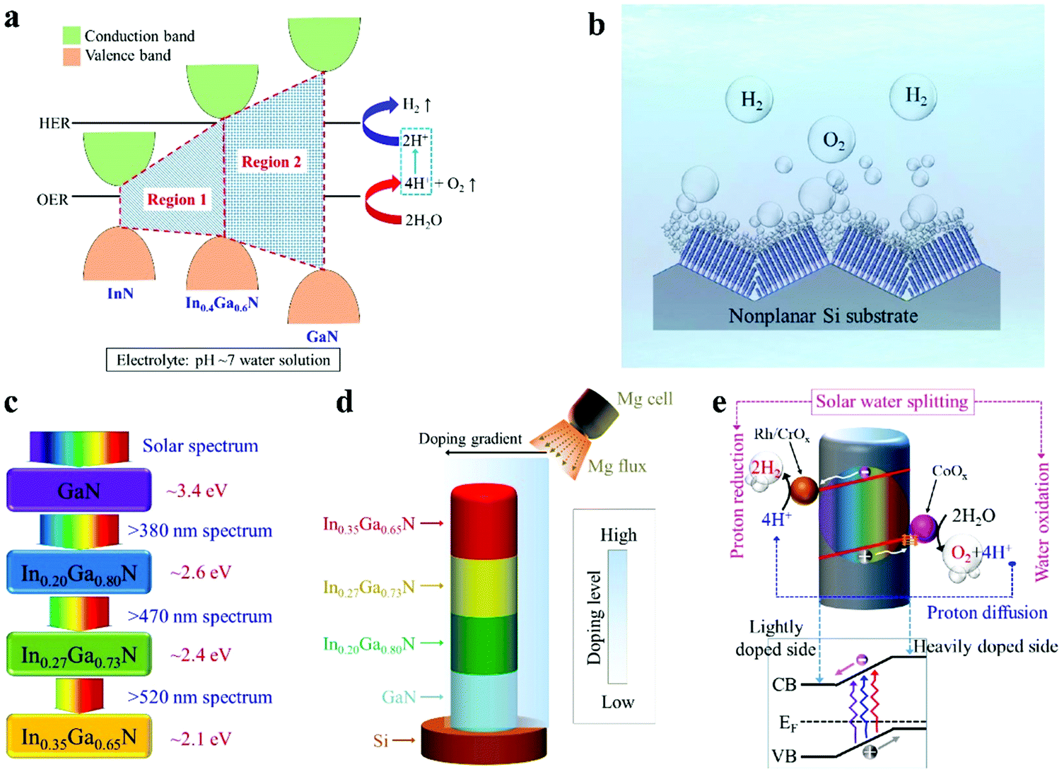 | ||
| Fig. 1 Schematic design and structural properties of monolithic multi-band metal nitride nanowire arrays for photocatalytic overall water splitting in nearly pH neutral electrolyte solution. (a) Band edge positions of GaN, InN, and their InGaN compounds. In liquid solution at pH ∼ 7, InGaN alloys with indium incorporation up to 40% can straddle the water redox reaction, noted as Region 2. Higher indium incorporation (Region 1) makes InGaN compounds unsuitable for overall solar water splitting. (b) Schematic illustration of photocatalytic water splitting on InGaN nanowire arrays monolithically integrated on a nonplanar Si wafer. (c) Schematic illustration of the ideal configuration for light absorption on the multi-band InGaN stacks with varied indium compositions. (d) Schematic of the quadruple-band InGaN nanowire. The p-type dopant originating from the tilted Mg effusion cell (relative to the nanowire orientation) leads to the Mg doping gradient profile in the lateral direction of the nanowire, which can introduce a built-in electric field, illustrated in (e), for efficient charge carrier separation and extraction for water redox reactions. | ||
Significantly, due to the use of a nonplanar Si wafer and the formation of nanowires vertically aligned to the local surfaces (Fig. 1b), only one side of the nanowires is directly exposed to Mg doping flux during nanowire epitaxial growth, as schematically shown in Fig. 1d. As such, an Mg doping gradient is spontaneously formed along the nanowire lateral dimension, which introduces a built-in electric field, as shown in Fig. 1e.34 It is seen that photo-generated electrons migrate towards the lightly Mg-doped side for the proton reduction reaction, whereas photo-generated holes drift to the more heavily Mg-doped surface for the water oxidation reaction. The rapid separation and extraction of photo-generated electrons and holes to the respective cathodic and anodic surfaces can significantly reduce charge carrier recombination and further suppress any back reaction, thereby leading to enhanced efficiency for solar water splitting.55–58
Scanning electron microscopy (SEM) images of metal–nitride nanowires grown on planar and nonplanar Si wafers are shown in Fig. 2a and b, respectively. The InGaN nanowires grown on a nonplanar Si wafer improve the hydrophilic property, as shown in the ESI,† Fig. S1, which may promote more efficient mass diffusion during solar water splitting. Strong photoluminescence (PL) emission spectra of single-band InGaN nanowires with various indium compositions were measured at room temperature, as shown in Fig. 2c, confirming the excellent material quality. By varying the growth conditions (see Methods), their energy bandgaps can be tuned from ∼3.4 eV to ∼2.1 eV, corresponding to PL emission wavelengths from ∼370 nm to ∼580 nm, respectively.39,59,60 For the PL emission at ∼580 nm, the corresponding indium composition is ∼35% (see the ESI,† Fig. S2).42
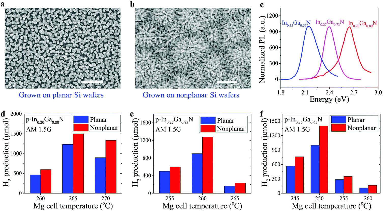 | ||
| Fig. 2 Properties and photocatalytic performance of single-band metal nitride nanowires grown on planar or nonplanar Si wafers, with different doping levels by varying the Mg effusion cell temperature. Electron microscopy images of InGaN nanowires grown on planar and nonplanar Si wafers. (a) Scale bar: 1 μm. (b) Scale bar: 1 μm. (c) Room-temperature photoluminescence (PL) spectrum of single-band InGaN nanowires with varied indium compositions of ∼20%, ∼27%, and ∼35%, corresponding to an energy gap of ∼2.6 eV, ∼2.4 eV, and ∼2.1 eV, respectively. (d–f) Summarized H2 gas production by photocatalytic pure water splitting on single-band p-In0.20Ga0.80N (d), p-In0.27Ga0.73N (e), and p-In0.35Ga0.65N (f) nanowires at varied Mg effusion cell temperatures on planar (blue bars) and nonplanar (red bars) Si wafers. H2 gas production was recorded after 40 minutes of the water splitting experiment. The sample sizes are ∼2.5–3 cm2. | ||
We have first performed photocatalytic water splitting studies on individual single-band InGaN nanowire photocatalysts with varied indium compositions and Mg-dopant incorporations (see Methods). The photocatalytic water splitting performance of p-In0.20Ga0.80N, p-In0.27Ga0.73N, and p-In0.35Ga0.65N, respectively, is summarized as shown in Fig. 2d–f, where samples with areal sizes ∼2.5–3 cm2 were used to optimize the doping condition. Recent studies suggest that Mg doping plays a critical role in the photocatalytic performance of III-nitride materials for overall solar water splitting.30,61 Therefore, we have firstly investigated and optimized the Mg doping effect on solar hydrogen gas production by varying the Mg doping flux (controlled by the Mg effusion cell temperature). The optimum Mg cell temperatures were identified to be ∼265 °C, 260 °C, and 250 °C for In0.20Ga0.80N, In0.27Ga0.73N, and In0.35Ga0.65N nanowire photocatalysts, respectively. An optimum level of Mg dopant concentration is required to minimize the surface band bending for the efficient extraction of photo-generated charge carriers, as reported previously.30,34,61 The optimum Mg doping levels, however, depend on indium composition and growth conditions (see Methods). In addition, a 20–40% higher hydrogen production rate was measured for InGaN photocatalysts grown on nonplanar Si wafers compared to those on planar Si wafers under optimized conditions, due to, in part, the enhanced charge carrier separation and extraction (Fig. 1e).
We have subsequently studied quadruple-band metal–nitride nanowire photocatalysts by monolithically integrating p-In0.35Ga0.65N, p-In0.27Ga0.73N, and p-In0.20Ga0.80N together on the p-GaN segment (see Fig. 1d), which can absorb incident light with wavelengths up to ∼600 nm. Shown in Fig. 3a are the SEM images of quadruple-band InGaN nanowires grown on a nonplanar Si substrate. The flower-shaped morphology of InGaN nanostructures can maximize the side surface exposed to incident light illumination. The multi-band InGaN nanowires were further characterized by scanning transmission electron microscopy (STEM) and energy-dispersive X-ray (EDX) spectroscopy. As shown in Fig. 3b, the brighter contrast in the top region of the nanowire indicates more indium incorporation due to the atomic number contrast nature in high angle annular dark-field (HAADF) imaging. The InGaN nanowire becomes wider in diameter along the growth direction (indicated by the white arrow). EDX line scans were performed along the axial and lateral directions of the InGaN nanowire. Variations in Ga Lα, In Lα, and N Kα characteristic signals are presented in Fig. 3c–f for EDX scans along Line 1, Line 2, Line 3, and Line 4 in Fig. 3b, respectively. Along the axial direction, the In Lα signal intensity gradually decreases, indicating the reduced concentration of In incorporation from top to bottom of the InGaN nanowire, corresponding to the design shown in Fig. 1d. There are four segments forming such quadruple-band InGaN nanowires, including (I) In0.35Ga0.65N, (II) In0.27Ga0.63N, (III) In0.20Ga0.80N, and (IV) GaN. For each InGaN segment, variations in the Ga Lα and In Lα characteristic signals along the nanowire lateral dimensions are measured and shown in Fig. 3d, e, and f, respectively. We have further performed atomic resolution HAADF-STEM imaging for InGaN crystals with various indium compositions, as shown in Fig. 3g–i. The periodic ordering of atoms further demonstrates the high crystallinity, which is critical to reduce the bulk recombination for efficient charge carrier extraction.
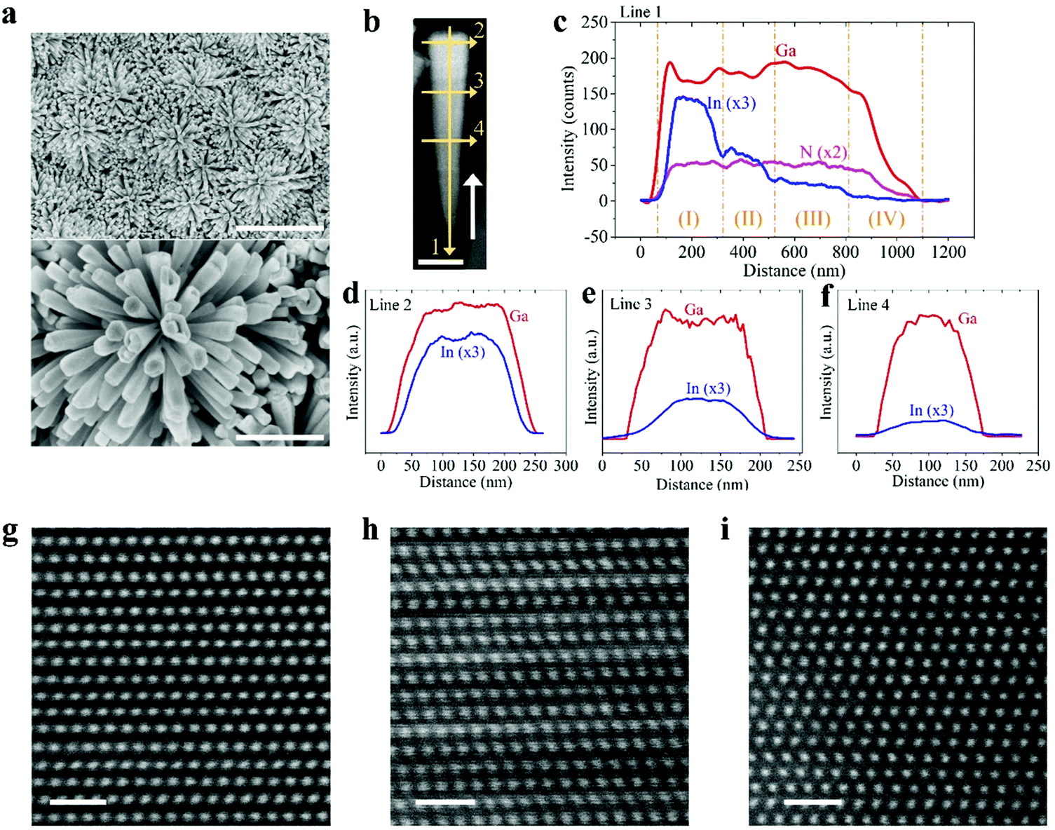 | ||
| Fig. 3 Structural characterization of the quadruple-band InGaN nanowire arrays monolithically integrated on a nonplanar Si wafer. (a) Top-view scanning electron microscopy (SEM) images of the flower-shaped InGaN nanowire structure grown on nonplanar Si substrates. Scale bar: 5 μm (top) and 1 μm (bottom). (b) Dark-filed scanning transmission electron microscopy (DF-STEM) image of the quadruple-band InGaN nanowire, with energy-dispersive X-ray spectroscopy (EDX) line scanning showing the variation of Ga Lα, In Lα, and N Kα characteristic signals along the axial and lateral directions. Scale bar: 200 nm. Spectra of Line 1 (c), Line 2 (d), Line 3 (e), and Line 4 (f) are measured along Arrow 1, Arrow 2, Arrow 3, and Arrow 4 in (b), respectively. (g–i) Atomic resolution STEM images of InGaN crystals for (g) In0.35Ga0.65N, (h) In0.27Ga0.73N, and (i) In0.20Ga0.80N segments, respectively. Scale bar: 1 nm. | ||
Schematically illustrated in Fig. 4a is the overall solar water splitting process on such quadruple-band InGaN nanowire photocatalysts under light illumination, including photon excitation in each single-band segment, charge carrier separation and extraction, and catalytic water splitting reactions. Due to the built-in electric field introduced by the Mg doping gradient profile, photo-generated electrons and holes are efficiently separated towards the cathodic surface driving the water reduction reaction and the anodic surface driving the water oxidation reaction, respectively.34,57 Furthermore, ESI,† Fig. S3 demonstrates the separate deposition of Rh and CoOx co-catalyst nanoparticles on the lightly and heavily Mg-doped InGaN surfaces, respectively, which indicates efficient charge carrier separation and extraction due to the Mg doping gradient along the lateral dimension of the nanowires. The rapid separation and extraction of photo-generated electrons and holes to the respective cathodic and anodic surfaces can significantly reduce charge carrier recombination and further suppress any back reaction.55–58 Shown in Fig. 4b is the PL spectrum of quadruple-band InGaN nanowires measured at room-temperature. The very broad emission spectrum indicates its capability of absorbing solar photons across nearly the entire visible spectrum. PL emission spectra of individual InGaN segments are also shown in Fig. 4b for comparison.
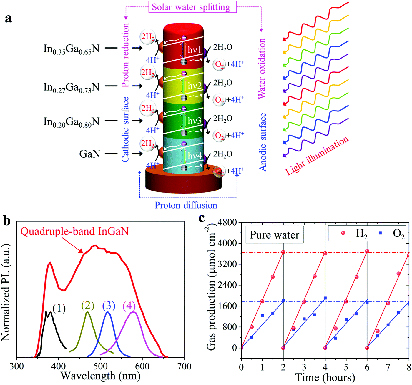 | ||
| Fig. 4 Photocatalytic performance of quadruple-band InGaN nanowire arrays measured in pure water by using a 300 W xenon lamp equipped with an AM 1.5G filter. (a) Schematic illustration of the overall water splitting process occurring on the quadruple-band nanowires under light illumination. (b) Room-temperature PL spectrum of the quadruple-band InGaN nanowires, compared to those of single-band nanowires, including (1) p-GaN, (2) p-In0.20Ga0.80N, (3) p-In0.27Ga0.73N, and (4) p-In0.35Ga0.65N. (c) H2 and O2 gas generation as a function of time measured in multiple cycles. | ||
Photocatalytic water splitting measurements of the quadruple-band nanowire arrays were performed in pH ∼ 7 pure water solution under concentrated light illumination using an AM 1.5G filter (see Methods). Shown in Fig. 4c is the H2 and O2 gas evolution for 120 minutes of continuous solar water splitting. Multiple cycles of photocatalytic experiments were further performed to confirm the stable, continuous gas production. The calculated H2 to O2 production ratio is nearly 2![[thin space (1/6-em)]](https://www.rsc.org/images/entities/char_2009.gif) :1, corresponding to the stoichiometric ratio in water molecules (H2O), which is consistent with the overall water splitting reaction occurring without any byproduct.5 The maximum H2 generation rate was measured to be ∼1840 μmol cm−2 h−1 corresponding to an STH efficiency of ∼5.2% (see Supplementary Note S1, ESI†).
:1, corresponding to the stoichiometric ratio in water molecules (H2O), which is consistent with the overall water splitting reaction occurring without any byproduct.5 The maximum H2 generation rate was measured to be ∼1840 μmol cm−2 h−1 corresponding to an STH efficiency of ∼5.2% (see Supplementary Note S1, ESI†).
As summarized in the ESI,† Table S1 is the performance comparison of some previously best-reported photocatalyst systems for overall solar water splitting, compared to the quadruple-band InGaN nanowire photocatalyst demonstrated in this work. To date, for III-nitride semiconductors, the best reported STH efficiency is 3.3% on double-band In0.22Ga0.78N/GaN photochemical diodes.34,41,45 For metal oxide and other nitride semiconductors showing comparable photocatalytic stability, e.g., SrTiO3, BiVO4, and C3N4,11,12,32,62–64 the highest STH efficiency has generally been limited to ∼1% mainly due to insufficient light absorption and strong recombination. Compared to the previously reported CoOx particulate system with ∼30 min stability,4 the presented quadruple-band metal–nitride nanowires demonstrate relatively good stability during overall solar water splitting, without showing any significant degradation of photocatalytic performance for ∼8 h. Compared to previously reported III-nitride photocatalysts, the significantly improved performance is attributed to the following factors: (1) the use of the quadruple-band structure to enhance visible light absorption and water redox reactions, (2) the use of the nonplanar wafer to enhance light absorption and trapping effect, and (3) controlled p-type dopant incorporation to enhance charge carrier separation and extraction. Theoretically, the ideal multi-band photocatalytic system in the current design can potentially reach a maximum energy conversion efficiency of ∼16% if all the incident photons above the energy bandgap can be converted to charge carriers to drive the water splitting reaction (see the ESI,† Fig. S4).65,66 Therefore, such multi-band nanostructures can be further optimized to achieve a possible STH efficiency >10%, which may include (1) optimization of the design by placing large energy gap materials on top, (2) optimization of the deposition of co-catalyst particles, (3) integration of such nanowire photocatalysts on the reflective substrate surface to further enhance light absorption, and (4) minimization of surface recombination by surface treatment or passivation. In addition, the STH efficiency may depend strongly on the light intensity, which needs to be studied in the future.
In summary, we have demonstrated wafer-level broadband InGaN nanowire photocatalysts that can significantly improve the efficiency of direct photocatalytic overall water splitting. Such photocatalyst materials can be synthesized on low cost, large area Si wafers utilizing industry standard manufacturing processes. Therefore, their large-scale manufacturability is unquestionable in the future. Significantly, with the incorporation of suitable co-catalysts, such a unique structure can be exploited to achieve high efficiency, stable artificial photosynthesis including one-step CO2 reduction to hydrocarbon fuels.41,67–79
Methods
Nonplanar Si surface preparation
A prime-grade polished silicon wafer was etched in 80 °C KOH solution (1.8% KOH in weight with 20% isopropanol in volume) for 30 minutes to form the micro-textured surface with Si pyramids.42 After being neutralized in concentrated hydrochloric acid, surface cleaning by acetone/methanol, and native oxide removal by 10% hydrofluoric acid, the nonplanar Si wafer was loaded into the MBE chamber for the growth of InGaN nanowires.Molecular beam epitaxial growth of multi-band InGaN nanowires
Mg doped (p-type) InGaN nanowires, single-band or multi-band structures, were grown on as-prepared nonplanar Si substrates by plasma-assisted molecular beam epitaxy (MBE) under N-rich conditions. The growth parameters include a gallium (Ga) beam equivalent pressure of ∼7 × 10⁻⁸ Torr, a nitrogen flow rate of 1 sccm, and a plasma power of 350 W. The substrate temperature, indium (In) beam equivalent pressure (BEP), and magnesium (Mg) cell temperature were tuned to synthesize different single-band or multi-band InGaN nanowires with various p-doping and alloy concentrations. For the single-band p-GaN nanowires, the substrate temperature was 685 °C and Ga BEP was ∼7 × 10⁻⁸ Torr. The p-type doping level was tuned by using different Mg cell temperatures. For the single-band p-In0.20Ga0.80N nanowires, the substrate temperature was 675 °C, Ga BEP was ∼7 × 10⁻⁸ Torr, and In BEP was ∼7.3 × 10⁻⁸. For single-band p-In0.27Ga0.73N nanowires, the substrate temperature was 662 °C, Ga BEP was ∼7 × 10⁻⁸ Torr, and In BEP was ∼7.3 × 10⁻⁸. For single-band p-In0.35Ga0.65N nanowires, the substrate temperature was 640 °C with Ga BEP ∼7 × 10⁻⁸ Torr and In BEP ∼3.5 × 10⁻⁸. For quadruple-band InGaN nanowires, the growth conditions are similar to those of the constituting single-band nanowires but with varying thicknesses for each segment. It is worth mentioning that the substrate temperature here refers to the thermocouple reading of the substrate heater, which may be different from the real substrate surface temperature, depending on the sample size, substrate holder, and mounting configuration, and therefore may vary somewhat from run to run.Cocatalyst nanoparticle deposition
Prior to photocatalytic water splitting experiments, metal nitride nanowires were decorated with hydrogen evolution reaction (HER) and oxygen evolution reaction (OER) cocatalyst nanoparticles for efficient water redox reactions using the photo-deposition method. InGaN samples were put in a glass chamber with a quartz lid, which was first pumped down and then illuminated using a 300 W Xenon lamp for 20 minutes to deposit cocatalyst nanoparticles on InGaN nanowires. The deposition of Rh/CrOx core/shell structures consists of two steps, including (1) the use of 55 mL of deionized water, 11 mL of methanol, and 2 μmol sodium hexachlororhodate (Na3RhCl6, Sigma-Aldrich) for the formation of the Rh core, and (2) the use of 55 mL of deionized water, 11 mL of methanol, and 4 μmol potassium chromate (K2CrO4, Sigma-Aldrich) for the CrOx shell. The deposition of CoOx nanoparticles involves the use of 60 mL of deionized water, 6 mL of potassium iodate (KIO3, 0.01 M, Sigma-Aldrich), and 4 μmol cobalt nitrate (Co(NO3)2, Alfa Aesar).Photocatalytic water splitting measurements
Photocatalytic overall water splitting measurements were conducted in a vacuum chamber with a quartz lid. The measurement chamber was partially filled with 70 mL of pure water solution (pH ∼ 7), which covered the InGaN photocatalysts, and was then pumped down. After evacuating the chamber, the sample was illuminated using a Xenon lamp (PE300BUV and CERMAX) together with various optical filters. With the use of an AM 1.5G filter, the light intensity is ∼2339 mW cm−2, equivalent to ∼23 suns, as measured at the sample position for the best performing sample. The light intensity was manually measured using a thermopile detector, which was covered using thick aluminum foil with an opening area similar to the sample size. It is important to mention that there may be ∼10–20% uncertainty in the measured light intensity due to spatial variations of the light intensity of the lamp and the exact positioning of the detector and sample. The water solution was purged using argon gas for 30 minutes before any experiments. H2 and O2 gas was analyzed by sampling using a vacuum-tight syringe and evaluating using a gas chromatograph machine (GC-8A, Shimadzu) equipped with a thermal conductivity detector (TCD) and high purity argon as the carrier gas. Extensive photocatalytic experiments were performed on quadruple-band InGaN samples with areal sizes in the range of 0.5–1 cm2 to identify the maximum STH efficiency.Structural and optical characterization
Room-temperature photoluminescence measurements of InGaN nanowires were performed in a homemade setup with a He–Cd 325 nm laser as the excitation source, and the emission is spectrally resolved using a SPEX spectrometer equipped with a photomultiplier tube. SEM images were recorded by employing a secondary electron detector using a Tescan MIRA3 system (15 kV) and a JEOL IT500 system (20 kV) with an EDX detector. High angle annular dark-field scanning transmission electron microscopy (HAADF-STEM) images were collected using a JEOL 3100R05 microscope operated at 300 keV in aberration corrected STEM mode with a beam convergence angle of 22 mrad and a detector collection angle of 85 mrad.Conflicts of interest
The authors declare no competing interests.Acknowledgements
This work was supported by the National Science Foundation under grant CBET 1804458. This work was performed in part at the University of Michigan Lurie Nanofabrication Facility. The authors acknowledge the financial support from the University of Michigan College of Engineering and technical support from the Michigan Center for Materials Characterization. The authors sincerely acknowledge the assistance from Mr Yazhou Zhang at Xi’an Jiaotong University, China for photocatalytic pure water splitting experiments on Mg doping optimization of single-band metal nitride nanowires.References
- A. Fujishima and K. Honda, Nature, 1972, 238, 37 CrossRef CAS.
- X. Chen, S. Shen, L. Guo and S. S. Mao, Chem. Rev., 2010, 110, 6503–6570 CrossRef CAS PubMed.
- C. F. Shih, T. Zhang, J. Li and C. Bai, Joule, 2018, 2, 1925–1949 CrossRef CAS.
- L. Liao, Q. Zhang, Z. Su, Z. Zhao, Y. Wang, Y. Li, X. Lu, D. Wei, G. Feng, Q. Yu, X. Cai, J. Zhao, Z. Ren, H. Fang, F. Robles-Hernandez, S. Baldelli and J. Bao, Nat. Nanotechnol., 2013, 9, 69 CrossRef PubMed.
- Y. Wang, S. Zhao, Y. Wang, D. A. Laleyan, Y. Wu, B. Ouyang, P. Ou, J. Song and Z. Mi, Nano Energy, 2018, 51, 54–60 CrossRef CAS.
- Z. Wang, Y. Inoue, T. Hisatomi, R. Ishikawa, Q. Wang, T. Takata, S. Chen, N. Shibata, Y. Ikuhara and K. Domen, Nat. Catal., 2018, 1, 756–763 CrossRef.
- K. Takanabe, ACS Catal., 2017, 7, 8006–8022 CrossRef CAS.
- B. A. Pinaud, J. D. Benck, L. C. Seitz, A. J. Forman, Z. Chen, T. G. Deutsch, B. D. James, K. N. Baum, G. N. Baum, S. Ardo, H. Wang, E. Miller and T. F. Jaramillo, Energy Environ. Sci., 2013, 6, 1983–2002 RSC.
- M. Grätzel, Nature, 2001, 414, 338 CrossRef.
- L. Yuan, C. Han, M.-Q. Yang and Y.-J. Xu, Int. Rev. Phys. Chem., 2016, 35, 1–36 Search PubMed.
- Q. Wang, T. Hisatomi, Q. Jia, H. Tokudome, M. Zhong, C. Wang, Z. Pan, T. Takata, M. Nakabayashi, N. Shibata, Y. Li, I. D. Sharp, A. Kudo, T. Yamada and K. Domen, Nat. Mater., 2016, 15, 611 CrossRef CAS PubMed.
- J. Liu, Y. Liu, N. Liu, Y. Han, X. Zhang, H. Huang, Y. Lifshitz, S.-T. Lee, J. Zhong and Z. Kang, Science, 2015, 347, 970 CrossRef CAS PubMed.
- K. Maeda, K. Teramura, D. Lu, T. Takata, N. Saito, Y. Inoue and K. Domen, Nature, 2006, 440, 295 CrossRef CAS PubMed.
- Z. Zou, J. Ye, K. Sayama and H. Arakawa, Nature, 2001, 414, 625 CrossRef CAS.
- S.-H. Li, N. Zhang, X. Xie, R. Luque and Y.-J. Xu, Angew. Chem., Int. Ed., 2018, 57, 13082–13085 CrossRef CAS.
- S. Y. Tee, K. Y. Win, W. S. Teo, L.-D. Koh, S. Liu, C. P. Teng and M.-Y. Han, Adv. Sci., 2017, 4, 1600337 CrossRef PubMed.
- A. Kudo and Y. Miseki, Chem. Soc. Rev., 2009, 38, 253–278 RSC.
- S. Liu, C. Han, Z.-R. Tang and Y.-J. Xu, Mater. Horiz., 2016, 3, 270–282 RSC.
- M. Ge, Q. Li, C. Cao, J. Huang, S. Li, S. Zhang, Z. Chen, K. Zhang, S. S. Al-Deyab and Y. Lai, Adv. Sci., 2016, 4, 1600152 CrossRef PubMed.
- Y. Goto, T. Hisatomi, Q. Wang, T. Higashi, K. Ishikiriyama, T. Maeda, Y. Sakata, S. Okunaka, H. Tokudome, M. Katayama, S. Akiyama, H. Nishiyama, Y. Inoue, T. Takewaki, T. Setoyama, T. Minegishi, T. Takata, T. Yamada and K. Domen, Joule, 2018, 2, 509–520 CrossRef CAS.
- S. P. Phivilay, C. A. Roberts, A. D. Gamalski, E. A. Stach, S. Zhang, L. Nguyen, Y. Tang, A. Xiong, A. A. Puretzky, F. F. Tao, K. Domen and I. E. Wachs, ACS Catal., 2018, 8, 6650–6658 CrossRef CAS.
- Z. Pan, T. Hisatomi, Q. Wang, S. Chen, A. Iwase, M. Nakabayashi, N. Shibata, T. Takata, M. Katayama, T. Minegishi, A. Kudo and K. Domen, Adv. Funct. Mater., 2016, 26, 7011–7019 CrossRef CAS.
- S. Liu, Z.-R. Tang, Y. Sun, J. C. Colmenares and Y.-J. Xu, Chem. Soc. Rev., 2015, 44, 5053–5075 RSC.
- Y. H. Lee, J. Kim and J. Oh, ACS Appl. Mater. Interfaces, 2018, 10, 33230–33237 CrossRef CAS PubMed.
- R. Fan, G. Huang, Y. Wang, Z. Mi and M. Shen, Appl. Catal., B, 2018, 237, 158–165 CrossRef CAS.
- M. H. Lee, K. Takei, J. Zhang, R. Kapadia, M. Zheng, Y.-Z. Chen, J. Nah, T. S. Matthews, Y.-L. Chueh, J. W. Ager and A. Javey, Angew. Chem., Int. Ed., 2012, 51, 10760–10764 CrossRef CAS PubMed.
- R. Chen, S. Pang, H. An, J. Zhu, S. Ye, Y. Gao, F. Fan and C. Li, Nat. Energy, 2018, 3, 655–663 CrossRef CAS.
- B. Wang, S. Shen and S. S. Mao, J. Materiomics, 2017, 3, 96–111 CrossRef.
- C. Pan, T. Takata, M. Nakabayashi, T. Matsumoto, N. Shibata, Y. Ikuhara and K. Domen, Angew. Chem., Int. Ed., 2015, 54, 2955–2959 CrossRef CAS PubMed.
- M. G. Kibria, S. Zhao, F. A. Chowdhury, Q. Wang, H. P. T. Nguyen, M. L. Trudeau, H. Guo and Z. Mi, Nat. Commun., 2014, 5, 3825 CrossRef CAS PubMed.
- N. Zhang, C. Han, Y.-J. Xu, J. J. Foley Iv, D. Zhang, J. Codrington, S. K. Gray and Y. Sun, Nat. Photonics, 2016, 10, 473 CrossRef CAS.
- Q. Wang, T. Hisatomi, Y. Suzuki, Z. Pan, J. Seo, M. Katayama, T. Minegishi, H. Nishiyama, T. Takata, K. Seki, A. Kudo, T. Yamada and K. Domen, J. Am. Chem. Soc., 2017, 139, 1675–1683 CrossRef CAS PubMed.
- X. Guan, F. A. Chowdhury, N. Pant, L. Guo, L. Vayssieres and Z. Mi, J. Phys. Chem. C, 2018, 122, 13797–13802 CrossRef CAS.
- F. A. Chowdhury, M. L. Trudeau, H. Guo and Z. Mi, Nat. Commun., 2018, 9, 1707 CrossRef PubMed.
- Y. L. Wang, T. Nie, Y. H. Li, X. L. Wang, L. R. Zheng, A. P. Chen, X. Q. Gong and H. G. Yang, Angew. Chem., Int. Ed., 2017, 56, 7430–7434 CrossRef CAS.
- E. Nurlaela, A. Ziani and K. Takanabe, Mater. Renew. Sustain. Energy, 2016, 5, 18 CrossRef.
- X. Jia, Y. Zhao, G. Chen, L. Shang, R. Shi, X. Kang, G. I. N. Waterhouse, L.-Z. Wu, C.-H. Tung and T. Zhang, Adv. Energy Mater., 2016, 6, 1502585 CrossRef.
- T. Ohno, L. Bai, T. Hisatomi, K. Maeda and K. Domen, J. Am. Chem. Soc., 2012, 134, 8254–8259 CrossRef CAS PubMed.
- T. Kuykendall, P. Ulrich, S. Aloni and P. Yang, Nat. Mater., 2007, 6, 951 CrossRef CAS PubMed.
- P. G. Moses, M. Miao, Q. Yan and C. G. Van de Walle, J. Chem. Phys., 2011, 134, 084703 CrossRef PubMed.
- M. G. Kibria and Z. Mi, J. Mater. Chem. A, 2016, 4, 2801–2820 RSC.
- Y. Wang, S. Vanka, J. Gim, Y. Wu, R. Fan, Y. Zhang, J. Shi, M. Shen, R. Hovden and Z. Mi, Nano Energy, 2019, 57, 405–413 CrossRef CAS.
- M. G. Kibria, H. P. T. Nguyen, K. Cui, S. Zhao, D. Liu, H. Guo, M. L. Trudeau, S. Paradis, A.-R. Hakima and Z. Mi, ACS Nano, 2013, 7, 7886–7893 CrossRef CAS PubMed.
- D. Wang, A. Pierre, M. G. Kibria, K. Cui, X. Han, K. H. Bevan, H. Guo, S. Paradis, A.-R. Hakima and Z. Mi, Nano Lett., 2011, 11, 2353–2357 CrossRef CAS PubMed.
- X. Guan, F. A. Chowdhury, Y. Wang, N. Pant, S. Vanka, M. L. Trudeau, L. Guo, L. Vayssieres and Z. Mi, ACS Energy Lett., 2018, 3, 2230–2231 CrossRef CAS.
- M. G. Kibria, F. A. Chowdhury, M. L. Trudeau, H. Guo and Z. Mi, Nanotechnology, 2015, 26, 285401 CrossRef CAS.
- S. Rajaambal, M. Mapa and C. S. Gopinath, Dalton Trans., 2014, 43, 12546–12554 RSC.
- Y. Cui, L. Peng, L. Sun, Q. Qian and Y. Huang, J. Mater. Chem. A, 2018, 6, 22768–22777 RSC.
- P. G. Moses and C. G. Van de Walle, Appl. Phys. Lett., 2010, 96, 021908 CrossRef.
- F. A. Chowdhury, Z. Mi, M. G. Kibria and M. L. Trudeau, APL Mater., 2015, 3, 104408 CrossRef.
- S. Chen, T. Takata and K. Domen, Nat. Rev. Mater., 2017, 2, 17050 CrossRef CAS.
- D.-H. Tu, H.-C. Wang, P.-S. Wang, W.-C. Cheng, K.-H. Chen, C.-I. Wu, S. Chattopadhyay and L.-C. Chen, Int. J. Hydrogen Energy, 2013, 38, 14433–14439 CrossRef CAS.
- E. Garnett and P. Yang, Nano Lett., 2010, 10, 1082–1087 CrossRef CAS.
- L. Meng, Y. Zhang and C. Yam, J. Phys. Chem. Lett., 2017, 8, 571–575 CrossRef CAS PubMed.
- Q. Shi, S. Murcia-López, P. Tang, C. Flox, J. R. Morante, Z. Bian, H. Wang and T. Andreu, ACS Catal., 2018, 8, 3331–3342 CrossRef CAS.
- L. I. Granone, F. Sieland, N. Zheng, R. Dillert and D. W. Bahnemann, Green Chem., 2018, 20, 1169–1192 RSC.
- R. Marschall, Adv. Funct. Mater., 2014, 24, 2421–2440 CrossRef CAS.
- F. Le Formal, S. R. Pendlebury, M. Cornuz, S. D. Tilley, M. Grätzel and J. R. Durrant, J. Am. Chem. Soc., 2014, 136, 2564–2574 CrossRef CAS PubMed.
- R. R. Pelá, C. Caetano, M. Marques, L. G. Ferreira, J. Furthmüller and L. K. Teles, Appl. Phys. Lett., 2011, 98, 151907 CrossRef.
- I. Vurgaftman and J. R. Meyer, J. Appl. Phys., 2003, 94, 3675–3696 CrossRef CAS.
- M. G. Kibria, F. A. Chowdhury, S. Zhao, B. AlOtaibi, M. L. Trudeau, H. Guo and Z. Mi, Nat. Commun., 2015, 6, 6797 CrossRef CAS PubMed.
- A. Nakada, S. Nishioka, J. J. M. Vequizo, K. Muraoka, T. Kanazawa, A. Yamakata, S. Nozawa, H. Kumagai, S.-I. Adachi, O. Ishitani and K. Maeda, J. Mater. Chem. A, 2017, 5, 11710–11719 RSC.
- R. Asai, H. Nemoto, Q. Jia, K. Saito, A. Iwase and A. Kudo, Chem. Commun., 2014, 50, 2543–2546 RSC.
- Y. Wang, F. Silveri, M. K. Bayazit, Q. Ruan, Y. Li, J. Xie, C. R. A. Catlow and J. Tang, Adv. Energy Mater., 2018, 8, 1801084 CrossRef.
- J. Juodkazytė, G. Seniutinas, B. Šebeka, I. Savickaja, T. Malinauskas, K. Badokas, K. Juodkazis and S. Juodkazis, Int. J. Hydrogen Energy, 2016, 41, 11941–11948 CrossRef.
- K. T. Fountaine, H. J. Lewerenz and H. A. Atwater, Nat. Commun., 2016, 7, 13706 CrossRef CAS PubMed.
- S. Chu, P. Ou, P. Ghamari, S. Vanka, B. Zhou, I. Shih, J. Song and Z. Mi, J. Am. Chem. Soc., 2018, 140, 7869–7877 CrossRef CAS PubMed.
- J. K. Sheu, P. H. Liao, T. C. Huang, K. J. Chiang, W. C. Lai and M. L. Lee, Sol. Energy Mater. Sol. Cells, 2017, 166, 86–90 CrossRef CAS.
- Y. Wang, S. Fan, B. AlOtaibi, Y. Wang, L. Li and Z. Mi, Chem. – Eur. J., 2016, 22, 8809–8813 CrossRef CAS PubMed.
- T. Sekimoto, H. Hashiba, S. Shinagawa, Y. Uetake, M. Deguchi, S. Yotsuhashi and K. Ohkawa, J. Phys. Chem. C, 2016, 120, 13970–13975 CrossRef CAS.
- S. Chu, S. Fan, Y. Wang, D. Rossouw, Y. Wang, G. A. Botton and Z. Mi, Angew. Chem., Int. Ed., 2016, 55, 14262–14266 CrossRef CAS PubMed.
- B. AlOtaibi, X. Kong, S. Vanka, S. Y. Woo, A. Pofelski, F. Oudjedi, S. Fan, M. G. Kibria, G. A. Botton, W. Ji, H. Guo and Z. Mi, ACS Energy Lett., 2016, 1, 246–252 CrossRef CAS.
- Y. Wang, B. AlOtaibi, F. A. Chowdhury, S. Fan, M. G. Kibria, L. Li, C.-J. Li and Z. Mi, APL Mater., 2015, 3, 116106 CrossRef.
- T. Sekimoto, S. Shinagawa, Y. Uetake, K. Noda, M. Deguchi, S. Yotsuhashi and K. Ohkawa, Appl. Phys. Lett., 2015, 106, 073902 CrossRef.
- B. AlOtaibi, S. Fan, D. Wang, J. Ye and Z. Mi, ACS Catal., 2015, 5, 5342–5348 CrossRef CAS.
- S. Yotsuhashi, M. Deguchi, Y. Yamada and K. Ohkawa, AIP Adv., 2014, 4, 067135 CrossRef.
- S. Yotsuhashi, M. Deguchi, Y. Zenitani, R. Hinogami, H. Hashiba, Y. Yamada and K. Ohkawa, Jpn. J. Appl. Phys., 2012, 51, 02BP07 CrossRef.
- S. Yotsuhashi, M. Deguchi, H. Hashiba, Y. Zenitani, R. Hinogami, Y. Yamada and K. Ohkawa, Appl. Phys. Lett., 2012, 100, 243904 CrossRef.
- S. Yotsuhashi, M. Deguchi, Y. Zenitani, R. Hinogami, H. Hashiba, Y. Yamada and K. Ohkawa, Appl. Phys. Express, 2011, 4, 117101 CrossRef.
Footnote |
| † Electronic supplementary information (ESI) available. See DOI: 10.1039/c9mh00257j |
| This journal is © The Royal Society of Chemistry 2019 |