
Photoluminescence manipulation of WS2 flakes by an individual Si nanoparticle†
Churong
Ma
 ,
Jiahao
Yan
,
Yingcong
Huang
and
Guowei
Yang
*
,
Jiahao
Yan
,
Yingcong
Huang
and
Guowei
Yang
*
State Key Laboratory of Optoelectronic Materials and Technologies, Nanotechnology Research Center, School of Materials Science & Engineering, Sun Yat-sen University, Guangzhou 510275, Guangdong, P. R. China. E-mail: stsygw@mail.sysu.edu.cn
First published on 21st September 2018
Abstract
Optical manipulation of photoluminescence (PL) emission in 2D materials through nanophotonic structures has attracted a lot of attention. However, it has not been achieved through individual all-dielectric nanoparticles (NPs) so far. Here, we put forward a new hybrid system to manipulate the PL emission, which is composed of an individual Si NP deposited on WS2 flakes of different thicknesses. For monolayer WS2 (1L-WS2), PL quenching accompanied by broadening and redshift is observed when integrated with Si NPs. In contrast, the PL of multilayer WS2 (ML-WS2) is significantly enhanced with the help of Si NPs. The PL manipulation of 1L- and ML-WS2 is attributed to the heating and strain effects due to the presence of Si NPs as well as the interaction between the localized field induced by Si NPs and the exciton dipoles in the WS2 flakes. Based on Mie resonances, Si NPs can be effectively heated up by laser pulses. The localized high temperature and strain enable the 1L-WS2 to transform from a direct to an indirect bandgap, resulting in PL quenching and redshift. On the other hand, the out-of-plane oriented exciton dipoles in ML-WS2 are easier to couple with the resonant optical field in Si NPs than the in-plane oriented exciton dipoles in 1L-WS2, which brings about strong field enhancement in favor of PL emission. The new hybrid system is promising for photodetection and on-chip circuit integration.
Conceptual insightsAs we know, two-dimensional transition-metal dichalcogenides (2D TMDCs) have emerged as a new platform for atomic-scale research in recent years by virtue of their unique electronic and optical properties, and understanding and manipulating the excitons in 2D materials are crucial to apply them for future photonic and optoelectronic integrations. As one of the most important exciton effects, PL emission and its manipulation have attracted a great deal of attention. In this work, we, for the first time, put forward a new hybrid system to manipulate the PL emission, which is composed of an individual Si nanoparticle (NP) deposited on WS2 flakes of different thicknesses. We demonstrate that, for a WS2 monolayer (1L), PL quenching accompanied by broadening and red-shift is observed when integrated with Si NPs. In contrast, the PL of a WS2 multilayer (≥2L) is significantly enhanced due to the presence of Si NPs. We also establish that the different responses of the WS2 monolayer and multilayer are attributed to the heating effect in Si NPs and the interaction between the localized field induced by Si NPs and the exciton dipoles in WS2 flakes. |
Introduction
Two-dimensional transition-metal dichalcogenides (2D TMDCs) have emerged as a new platform for atomic-scale research in recent years by virtue of their unique electronic and optical properties.1–3 They have been widely used in various photonics and optoelectronics devices4 such as single-photon emitters,5 light-emitting diodes,6 lasers,7 field-effect transistors8 and so on. When thinned from bulk to atomic-layer thickness, the material transforms from an indirect to a direct bandgap.9,10 Their excellent properties are usually associated with excitons.11 Hence, understanding and manipulating the excitons in 2D materials are crucial to apply them for future photonic and optoelectronic integrations. As one of the most important exciton effects, PL emission and its manipulation have attracted a great deal of attention. Traditionally, the PL emission in 2D materials can be controlled by thickness,12 substrate,13 strain14 and temperature.15 However, these conditions are hard to precisely handle or accomplish in practice, which prompted us to explore new approaches for PL manipulation.Recently, coupling 2D TMDCs to various nanophotonic structures like photonic crystal,16–18 plasmonic19–21 and all-dielectric nanostructures22,23 has been a promising approach to effectively manipulate the PL emission. For example, PL enhancement or quenching can be achieved in Au-MoS2 hybrid nanostructures via localized surface plasmons in noble metal nanoantennas.19,20 PL broadening and redshift have also been observed in this system, which is derived from the plasmonic heating effect.20 In addition, double resonances at both the excitation and emission wavelengths were engineered in photonic crystal and all-dielectric nanostructures to enhance the optical absorption and spontaneous emission rate of 2D TMDCs.17,22 Nevertheless, to date, the optical manipulation of PL emission in 2D TMDCs by an individual all-dielectric NP has not been reported.
Great attention has been paid to all-dielectric nanostructures in the past few years. Compared with plasmonic nanostructures, all-dielectric nanostructures do not suffer from high cost or high energy dissipation in the visible region, and they offer the opportunity for simultaneously supporting strong electric and magnetic Mie resonances.24 By virtue of their unique properties, all-dielectric nanostructures have been applied for directional scattering,25 optical sensors,26 nonlinear optics27 and so on.28 As a representative of all-dielectric nanomaterials, Si has been the most studied material because of its high refractive index,29 the mature fabrication technology and its compatibility for on-chip circuit integration.30 However, due to the indirect bandgap electronic structure of Si, integration with other direct bandgap materials is urgently required to generate light.22 In such cases, it is an effective solution to integrate Si nanostructures with 2D TMDCs.
In this contribution, we establish a hybrid system composed of individual Si NPs deposited on WS2 flakes of different thicknesses. With size increasing, the multipole Mie resonances of the Si NPs shift gradually to overlap the PL excitation and emission wavelengths, which offers a favorable opportunity for investigation of the interaction between Si NPs and WS2 flakes. For 1L-WS2, the presence of Si NP enables its PL emission to maximally have a 70 nm wavelength redshift and 88% intensity quenching together with broadening. We attribute this PL manipulation to the heating and strain effects induced by Si NPs. When exposed to laser pulses, Si NPs can be effectively heated up because of Mie resonances. The localized high temperature and strain transform 1L-WS2 from a direct to an indirect bandgap, leading to PL quenching, redshift and broadening. While for the ML-WS2, we observed significantly enhanced PL emission with negligible broadening or redshift (<5 nm). The different PL emission behaviors in Si/WS2 hybrid systems can be explained by the coupling of the localized field in Si NPs and exciton dipoles in WS2 flakes. For Si/1L-WS2 heterostructures, the in-plane oriented exciton dipoles in 1L-WS2 can be hardly coupled to the optical field in Si NPs, which is polarized perpendicularly to the layer planes. In contrast, the out-of-plane oriented exciton dipoles in ML-WS2 facilitate the coupling with the external optical field, resulting in strong near-field enhancement in favor of PL emission. The new hybrid system consisting of individual all-dielectric NPs and WS2 flakes is promising for photodetection31,32 and on-chip circuit integration.33
Results and discussion
WS2 flakes from 1L to ML were obtained by mechanical exfoliation and deposited on a 300 nm SiO2/Si substrate. The thickness of the WS2 flakes can be roughly identified by optical microscopy relying on the optical contrast between a 2D material and the substrate,34 as shown in Fig. 1a–d, respectively. Fig. 1e–h show the accurate results measured by atomic force microscopy (AFM). Besides, their corresponding scanning electron microscopy (SEM) images are depicted in Fig. S1 (ESI†). Exciton is an essential concept in 2D materials and it can be reflected by PL emission. As presented in Fig. 1i, the PL spectra of WS2 flakes show a remarkable dependence on layer number. With the thickness increasing from 1L to ML, the A exciton peak of the WS2 flakes redshifts. Fig. 1j (black line) shows the rapid decrease of relative PL intensity with respect to 1L-WS2, demonstrating the transformation from a direct to an indirect bandgap. In contrast, another PL peak attributed to indirect bandgap emission in ML-WS2 (dashed line in Fig. 1i) increases and redshifts with the thickness, as shown in Fig. 1j (red line). Very recently, a new method for layer number identification of few-layer WS2 (FL-WS2) has been reported depending on the indirect transition PL peak-positions,35 which is in accordance with our results. Moreover, the PL spectra of the WS2 flakes have redshifts to varying degrees (Fig. S2, ESI†) as the laser power increases because of the laser heating. It can be seen that the influence of the laser heating effect on the position of the A exciton peak is diminished with the thickness. Similar results have been observed in the Raman spectra measurement of WS2 flakes, which is shown in Fig. S3 (ESI†). As the laser power increases, the in-plane (E12g) and out-of-plane (A1g) Raman modes of WS2 redshift slightly.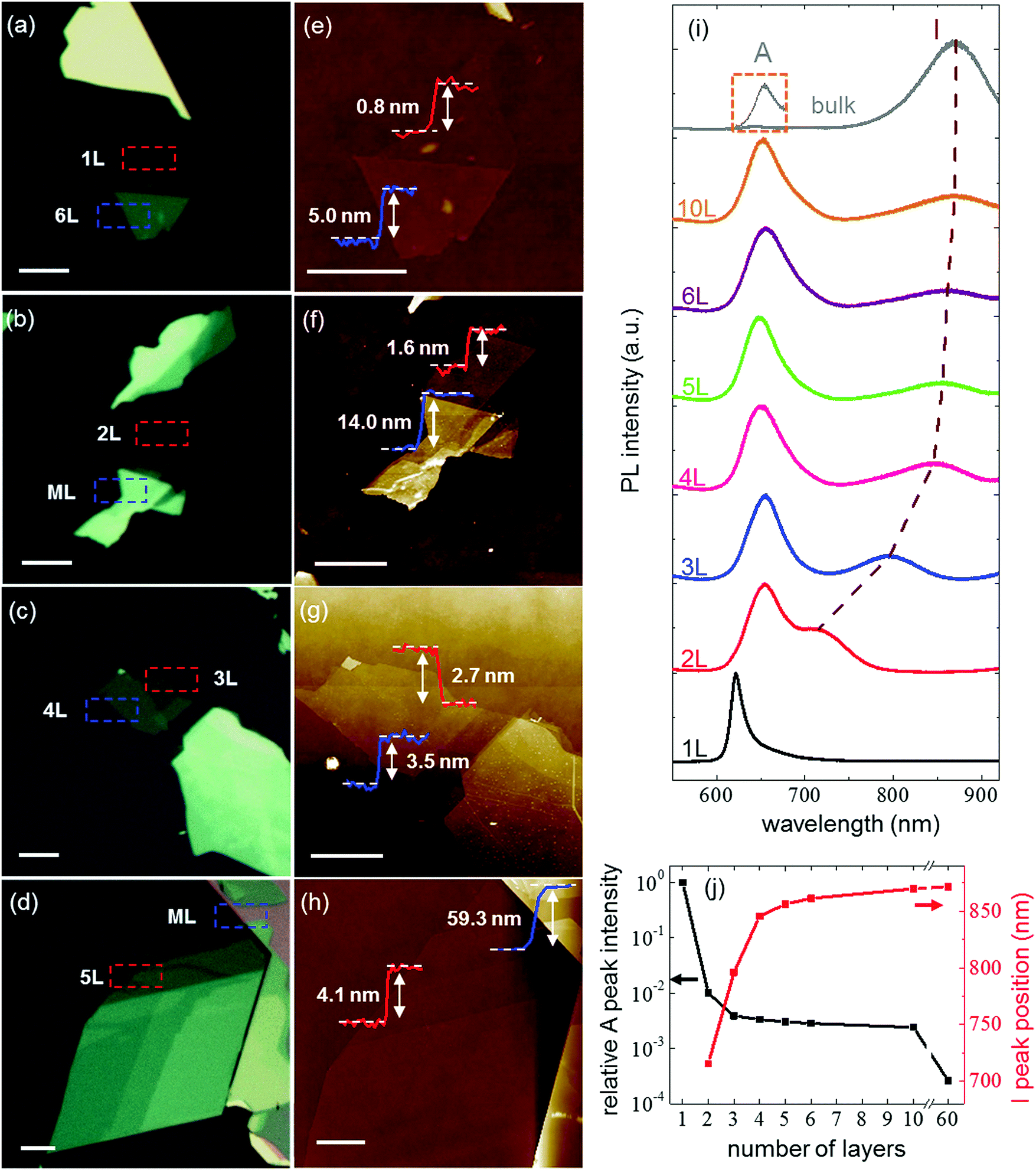 | ||
| Fig. 1 Characterization of WS2 flakes. (a–d) Bright-field optical microscopy images of WS2 flakes of different thicknesses on the 300 nm SiO2/Si substrate. The scale bar is 5 μm. (e–h) The corresponding AFM images including height profiles of WS2 flakes. The scale bar is 5 μm. (i) Normalized PL spectra of mechanically exfoliated WS2 flakes from 1L to bulk measured at the excitation laser power of 2 mW. The weak A exciton peak labeled by the dashed rectangle in WS2 bulk is magnified. The indirect transition PL peaks of WS2 flakes from 2L to bulk are connected by a dashed line. (j) Relative PL intensity of WS2 flakes (black line) and indirect transition PL peak positions extracted from (i) (red line). | ||
The Si NPs were fabricated by femtosecond laser ablation of Si wafer in deionized water.36 Fig. S4 (ESI†) shows the typical morphology and structure characterization of Si NPs. The SEM and transmission electron microscopy (TEM) images, X-ray diffraction (XRD) and selected-area electron diffraction (SAED) patterns demonstrate that the Si NPs we prepared are polycrystalline spheres with thin natural oxide layers (2–5 nm) on the surface. After the synthesis, we investigated the scattering behaviors of individual Si NPs on the 300 nm SiO2/Si substrate. As shown in Fig. 2, the scattering spectrum of Si NP exhibits a distinct redshift when it increases from 100 to 200 nm in diameter. The well-defined maximum at the long-wavelength spectral side can be attributed to magnetic dipole (MD) resonance and the neighboring maximum can be attributed to electric dipole (ED) resonance. Our experimental measurements shown in Fig. 2b agree well with the finite-difference time-domain (FDTD) simulations shown in Fig. 2c except the results located at around 400 nm because the quantum efficiency of our CCD drops quickly near the ultraviolet range. In addition, it is worth noting that the Si NPs can be heated up under the excitation of laser pulses depending on the electromagnetic resonance. Raman thermometry is often employed to interrogate the thermal response of micro- or nano-systems.37 As depicted in Fig. 2d, we observed that the Raman peak of Si NP gradually shifts down from 520.0 to 507.0 nm as size increases when exposed to a laser pulse at a power of 2 mW, which demonstrates that the temperature of the Si NPs is increased. According to previous work,37,38 the maximum temperature of Si NPs is estimated to be about 800 K.
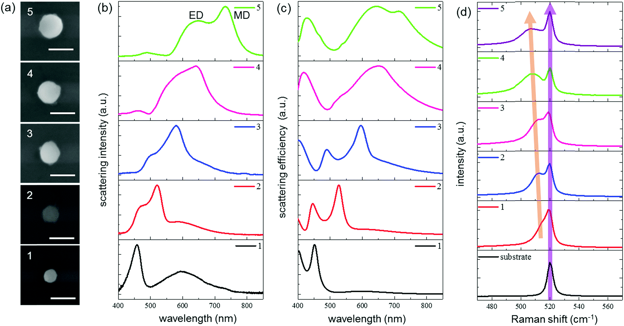 | ||
| Fig. 2 Scattering and Raman spectra of Si NPs on the 300 nm SiO2/Si substrate. (a) SEM images of Si NPs numbered from 1 to 5. The scale bar is 200 nm. (b) The measured scattering spectra of Si NPs selected in (a). (c) The corresponding FDTD simulated results. (d) The Raman spectra of the selected Si NPs. The orange and purple arrows indicate the Raman peaks of the Si NPs and SiO2/Si substrate, respectively. | ||
The Si/1L-WS2 hybrid system was studied first. Fig. 3a and b show the dark-field optical microscopy images of Si NPs of different sizes deposited on the selected 1L-WS2. Their corresponding SEM and bright-field optical microscopy images are presented in the insets at the bottom left corner, respectively. The SEM images of five selected Si/1L-WS2 heterostructures marked by white dotted circles in Fig. 3a and b are displayed in Fig. 3c. When these heterostructures are exposed to laser pulses, their PL emission spectra exhibit a pronounced quenching accompanied by broadening and wavelength redshift compared with the bare 1L-WS2, which is more and more apparent as Si NPs gradually increase from 103.4 to 200.0 nm, as depicted in Fig. 3d. The variations of PL intensity and peak position are shown in Fig. 3e. It can be seen that the PL emission of 1L-WS2 has a 70 nm wavelength redshift and 88% intensity quenching maximally. Furthermore, the PL mapping of the Si/1L-WS2 heterostructures is shown in Fig. S5 (ESI†).
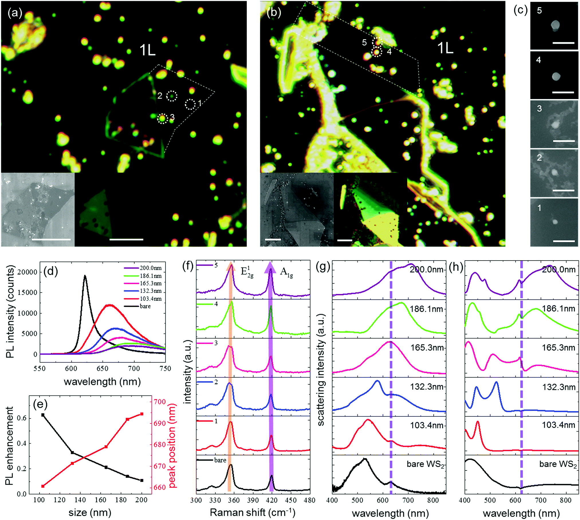 | ||
| Fig. 3 PL quenching in the Si/1L-WS2 hybrid systems. (a and b) The dark-field optical microscopy images of Si NPs deposited on 1L-WS2. The selected Si/1L-WS2 heterostructures are marked with white dashed circles and numbered from 1 to 5. Insets are the corresponding SEM and bright-field optical microscopy images. The scale bar is 5 μm. (c) SEM images of the typical heterostructures selected in (a and b). The scale bar is 500 nm. (d) PL spectra of the typical hybrid systems compared with the bare 1L-WS2. (e) PL quenching (black line) and peak position shift (red line) vary with the size of Si NPs. (f) The Raman spectra of the selected Si/1L-WS2 heterostructures compared with the bare 1L-WS2. The orange and purple arrows indicate the in-plane (E12g) and out-of-plane (A1g) Raman modes, respectively. (g) Scattering spectra of the Si/1L-WS2 heterostructures. The vertical dashed line located at 620 nm indicates the A excitonic resonance of 1L-WS2. (h) The corresponding FDTD simulated results. | ||
More information can be obtained from Raman spectra measurement. As shown in Fig. 3f, the Raman signals of Si/1L-WS2 heterostructures were measured compared with bare 1L-WS2. For both in-plane (E12g) and out-of-plane (A1g) modes, their Raman frequencies decrease due to the existence of Si NPs. It has been demonstrated that temperature rise15,39,40 or strain increase41,42 would result in redshifts of the Raman modes of 1L-WS2. Thus, we attribute the PL manipulation of 1L-WS2 to the heating and strain effects induced by Si NPs. On the one hand, as we demonstrated above, Si NPs can be effectively heated up under the excitation of laser pulses. Since 1L-WS2 has a low thermal conductivity of 32 W (m K)−1 at room temperature,40 it cannot dissipate the heat immediately, which leads to the temperature rise. Factors including thermal expansion of the lattice and anharmonic effects are responsible for the change of Raman frequency with increasing temperature. Temperature induced PL quenching in semiconductors typically results from direct or indirect thermal activation of non-radiative recombination processes associated with defects or impurities through emission of phonons.15 On the other hand, due to the presence of Si NPs, the induced strain will enable 1L-WS2 to transform from direct to indirect bandgap,41,43,44 which gives rise to a similar modulation of the lattice vibration and PL emission as high temperature. In addition, though the existence of an oxide layer presented on the surface of Si NPs can effectively prevent the carrier transfer between WS2 flakes and Si NPs, it is still possible for the carrier to tunnel into the other side. The photogenerated electrons and holes transfer between Si and WS2, leading to the PL quenching in 1L-WS2, as well.
To further understand the interaction between Si NPs and 1L-WS2, scattering spectra of the hybrid systems were investigated. The experimental results are shown in Fig. 3g. For the bare 1L-WS2, the spectral position of the A excitonic resonance can be obtained in its scattering spectrum (black line) measured from its edges. In our experiment, Mie resonances of Si NPs including ED and MD resonances can be tuned across the A exciton resonance. However, no distinct splitting peaks were observed, which demonstrates that strong coupling of Si NPs and 1L-WS2 was not achieved.45,46 In fact, it has been be proved that the nanocavity like NP-on-a-film cannot be employed to achieve strong coupling because polarization of the transition dipole moment is dominantly in-plane in 1L-TMDCs, which will not interact with the out-of-plane orientated electric field produced by the NPs.47,48 Moreover, true strong coupling can be reached only when the scattering data are accompanied by signs of polariton splitting in absorption49 or PL emission.50 Nevertheless, the polariton splitting was also not observed in the PL emission spectra of Si/1L-WS2 heterostructures (Fig. 3d). Fig. 3h shows the corresponding FDTD simulations. The discrepancy between experimental and simulated results is owing to the rapidly falling quantum efficiency of the CCD near the ultraviolet range (around 400 nm).
Different from Si/1L-WS2 heterostructures, we observed PL enhancements with negligible broadening and wavelength shift in the Si/ML-WS2 heterostructures. Fig. 4a and f show the dark-field optical microscopy images of Si-WS2 bilayer (Si/2L-WS2) and trilayer (Si/3L-WS2) hybrid systems combined with SEM and bright-field optical microscopy images, respectively. The marked heterostructures are displayed in Fig. 4b and g, respectively. For 2L-WS2, its PL emission intensity was slightly enhanced by Si NPs, which is shown in Fig. 4c and d. However, strong PL emission enhancement was achieved in 3L-WS2via the integration with Si NPs, as shown in Fig. 4h and i. The corresponding PL mapping is shown in Fig. S5 (ESI†). The enhanced interaction can be demonstrated by scattering spectra of the heterostructures as well. Fig. S6 (ESI†) shows the scattering spectra of bare WS2 flakes of different thicknesses. It can be seen that the A excitonic resonance peak becomes increasingly clear with thickness. Compared with a Si/1L-WS2 heterostructure, the interaction between Si NPs and FL-WS2 is strengthened since the splitting peak is increasingly visible when the MD resonance of Si NP was tuned to overlap the A excitonic resonance, which is shown in Fig. 4j. Meanwhile, we found that the PL enhancement reaches a maximum (1.7 times of the bare 3L-WS2, green line in Fig. 4h) because of this spectral overlap. The same conclusion can be drawn in Si/4L-WS2 heterostructures, as shown in Fig. S7 (ESI†).
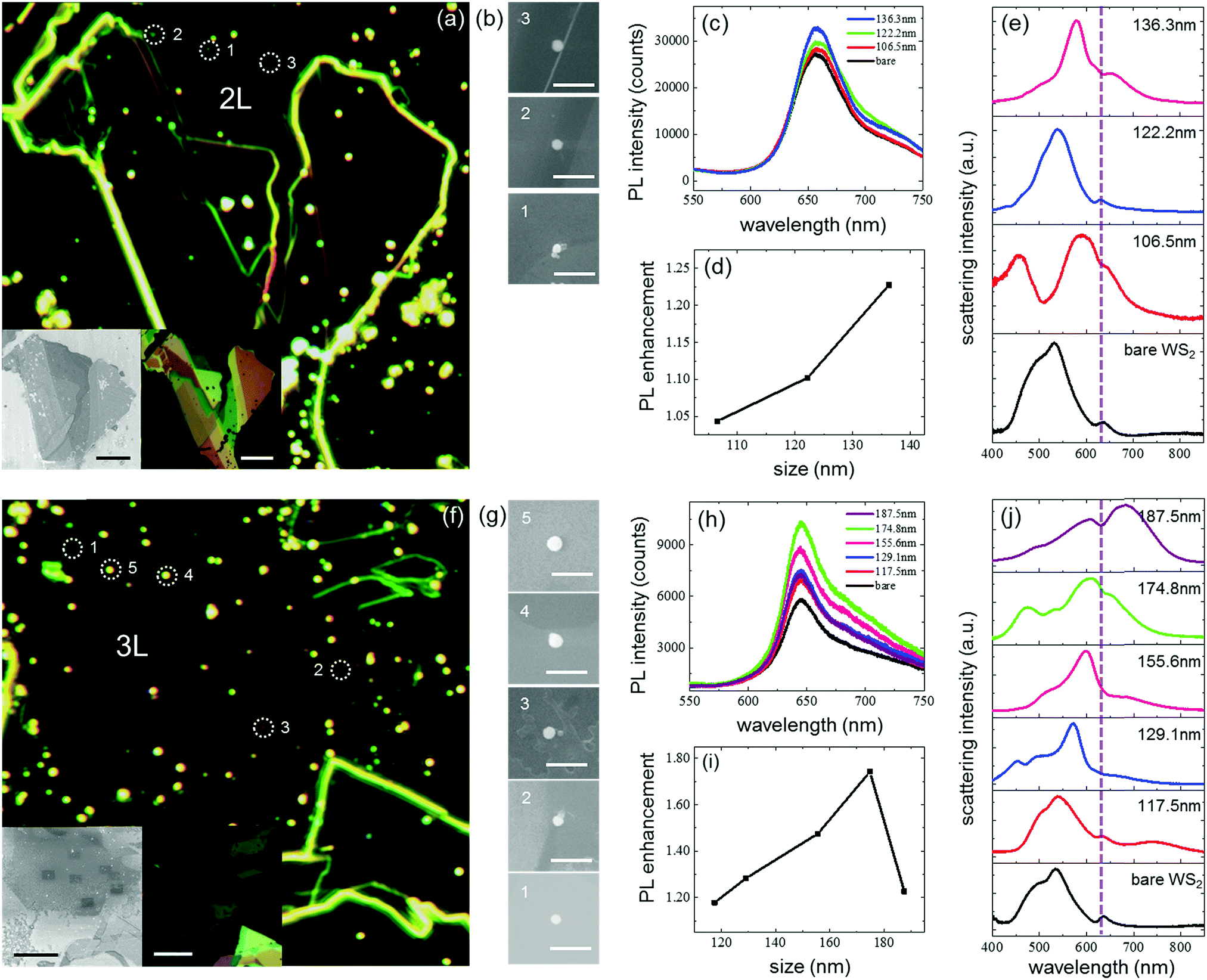 | ||
| Fig. 4 PL enhancement in the Si/FL-WS2 hybrid systems. (a and f) The dark-field optical microscopy images of Si/2L-WS2 and Si/3L-WS2 hybrid systems, respectively. The selected heterostructures are marked with white dashed circles and numbered. Insets are the corresponding SEM and bright-field optical microscopy images. The scale bar is 10 μm. (b and g) SEM images of the heterostructures selected in (a and f), respectively. The scale bar is 500 nm. (c and h) PL spectra of the selected heterostructures compared with the bare 2L- and 3L-WS2, respectively. (d and i) PL enhancement of the heterostructures varies with the size of the Si NPs. (e and j) The measured scattering spectra of the Si/FL-WS2 heterostructures. The vertical dashed lines located at around 640 nm indicate the A excitonic resonance in FL-WS2. | ||
More prominent PL enhancement of WS2 flakes was achieved when the thickness of the WS2 flake further increases. As shown in Fig. 5a and b, Si NPs were deposited on the ML-WS2 flakes (∼15.2 nm obtained by AFM results shown in Fig. S8, ESI†) to form the hybrid systems. Compared with Si/FL-WS2, we observed stronger PL enhancement in this hybrid system, which is presented in Fig. 5d and e. The PL emission of the ML-WS2 maximally increases by 4.0 times when integrated to a 170.5 nm Si NP (pink line, Fig. 5d). Its corresponding PL mapping is shown in Fig. S5 (ESI†). In addition, we observed a more obvious splitting peak located at around 640 nm in the scattering spectra of Si/ML-WS2 heterostructures when the MD resonance of the Si NP matches the A excitonic resonance, as shown in Fig. 5f (pink line). Similarly, it has been demonstrated that Rabi splitting can be achieved in ML-WSe2 (>7L) rather than 1L-WSe2 though its PL is weaker by reason of exciton recombination.48
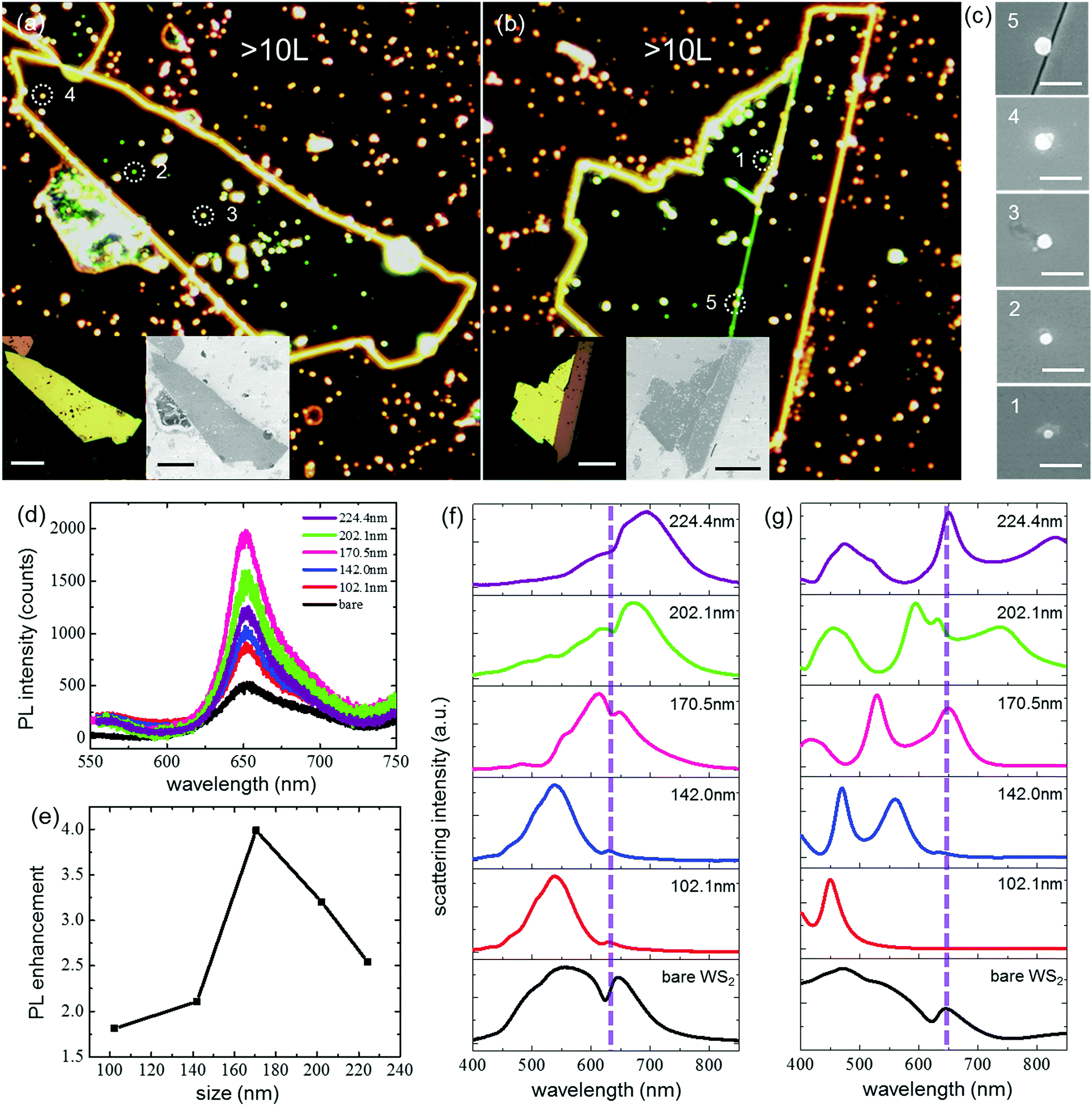 | ||
| Fig. 5 PL enhancement in the Si/ML-WS2 (>10L) hybrid systems. (a and b) The dark-field optical microscopy images of the Si/ML-WS2 hybrid systems. The selected heterostructures are marked with white dashed circles and numbered from 1 to 5. Insets are the corresponding SEM and bright-field optical microscopy images. The scale bar is 10 μm. (c) SEM images of the typical heterostructures selected in (a and b), respectively. The scale bar is 500 nm. (d) PL spectra of the selected heterostructures compared with the bare ML-WS2. (e) PL enhancement of the heterostructures varies with the size of the Si NPs. (f) The measured scattering spectra of the Si/ML-WS2 heterostructures. The vertical dashed lines located at around 642 nm indicate the A excitonic resonance in ML-WS2. (g) The corresponding FDTD simulated results. | ||
The aforementioned heating and strain effects induced by Si NPs enable 1L-WS2 to transform from a direct to an indirect bandgap, resulting in the PL quenching, redshift and broadening. However, these two effects have little influence on the PL emission of ML-WS2 due to the inherent indirect bandgap electronic structure and the larger thermal conductivity of ML-WS2.40,51 Another important factor is the interaction between Si NPs and WS2 flakes. From the far-field scattering results, we have come to a conclusion that the coupling of MD resonance and A excitonic resonance is enhanced with the thickness of the WS2 flakes. The out-of-plane oriented exciton dipoles in ML-WS2 prefer to couple with the localized field produced by Si NPs rather than the in-plane oriented exciton dipoles in 1L-WS2. From another point of view, the interaction between Si NPs and WS2 flakes can be described by near-field enhancement. Fig. 6a represents the schematic diagram of Si/WS2 hybrid systems. Si NPs of specific sizes are simulated to match their ED or MD resonances to the excitation wavelength (514 nm) and A excitonic resonance (620 nm for 1L-WS2 and 642 nm for ML-WS2) in WS2 flakes, as shown in Fig. 6b and c. The calculated multipolar contributions of Si NPs based on Mie theory are shown in Fig. S9 (ESI†). Light harvesting and optical absorption of WS2 flakes can be promoted due to strong field enhancement derived from the resonance at excitation wavelength.20,52 In fact, for non-magnetic materials, the absorbed electromagnetic power can be simply calculated by the equation53 , where ω is the angular frequency, Im(ε) is the imaginary part of the permittivity of WS2 flakes and |E| is the electric field amplitude. The field enhancements in the Si/1L-WS2 and Si/ML-WS2 heterostructures are displayed in Fig. 6d–i and j–o, respectively. We can see that the latter are generally greater than the former, which demonstrates that the interaction is stronger. In addition, the different PL enhancements controlled by Si NPs of different sizes can be explained by the field enhancement variation. On the other hand, a strong electric field will lead to the accelerated emission rate in WS2 flakes on account of the Purcell effect.54,55 The time-resolved spectra of Si/WS2 heterostructures are shown in Fig. S10 (ESI†). It can be seen that the spontaneous emission rate of a Si/WS2 heterostructure is increased compared with bare WS2.
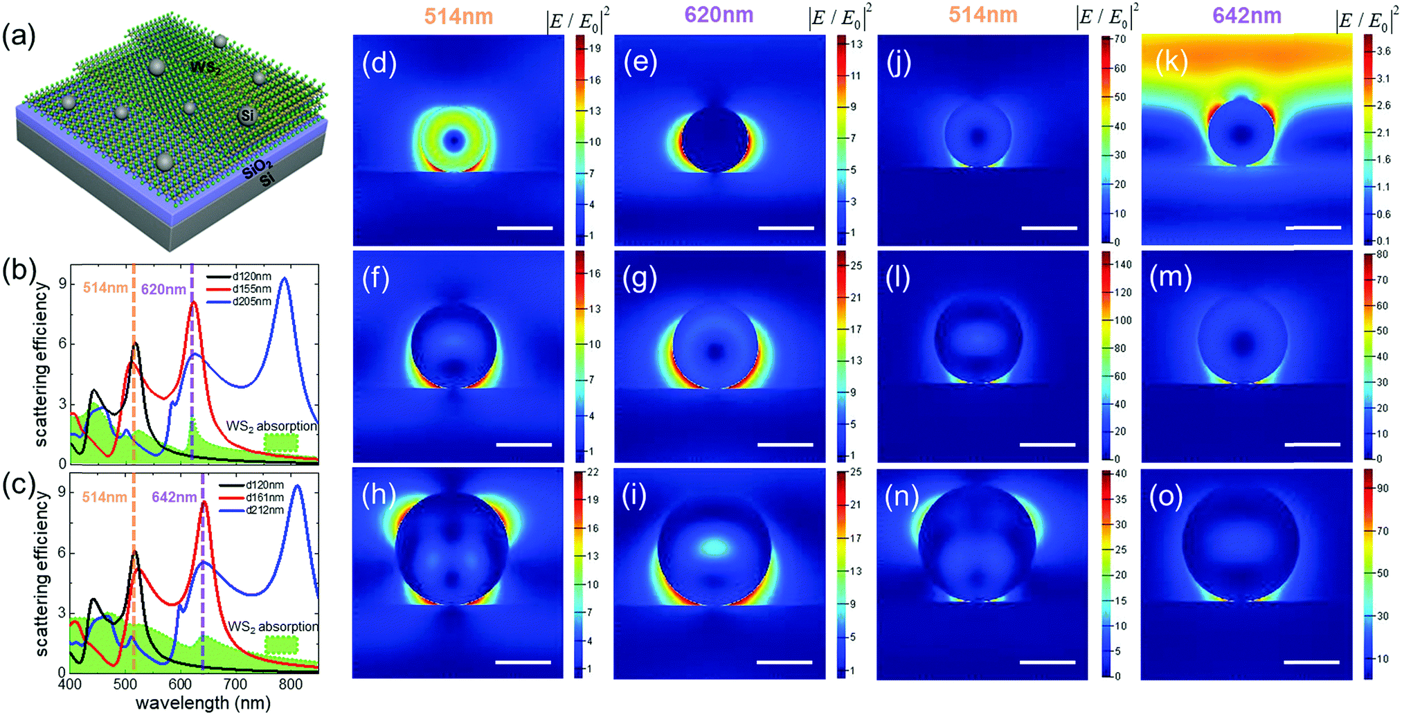 | ||
| Fig. 6 The near-field interaction between Si NPs and WS2 flakes on the 300 nm SiO2/Si substrate. (a) Schematic diagram of the hybrid systems composed of Si NPs and WS2 flakes. (b and c) Scattering efficiency of Si NPs whose Mie resonances overlap the PL excitation wavelength (514 nm) and A excitonic resonance in 1L-WS2 (620 nm) and ML-WS2 (642 nm), respectively. The green areas indicate the absorption of 1L- and ML-WS2, respectively. (d–i), (j–o) The electric field enhancements of the Si/1L-WS2 and Si/ML-WS2 hybrid systems at the PL excitation wavelength and A excitonic resonance, respectively. | ||
Conclusions
In summary, we have achieved the PL manipulation of WS2 flakes by individual Si NPs. The heating and strain effects induced by Si NPs enable PL emission of the 1L-WS2 to have a 70 nm wavelength redshift and 88% intensity quenching maximally. Meanwhile, PL emission of the ML-WS2 is strongly enhanced by Si NPs, which is more prominent with increasing thickness. The interaction between Si NPs and WS2 flakes has been investigated through the far-field scattering measurements and near-field FDTD simulations. In the far-field, the splitting peak in the scattering spectrum of a Si/WS2 heterostructure is increasingly visible as the WS2 flake increases from 1L to ML, indicating the strengthened coupling of MD resonance in Si NPs and A excitonic resonance in WS2 flakes. In the near-field, the field enhancement in a Si/ML-WS2 heterostructure is much stronger than that in a Si/1L-WS2 heterostructure, which can largely enhance the optical absorption and emission rate of the WS2 flakes in favor of PL emission. Essentially, exciton dipoles oriented in-plane in 1L-WS2 could be poorly coupled to the optical field polarized perpendicularly to the layer planes produced by Si NPs. In contrast, exciton dipoles in ML-WS2 are out-of-plane oriented, which boosts their interaction. The new hybrid system consisting of individual all-dielectric NPs and 2D materials is promising for photodetection and on-chip circuit integration.Experimental section
Fabrication of the samples
The WS2 flakes were mechanically exfoliated from the bulk crystal and transferred onto a Si substrate with 300 nm oxide thickness. Si NPs with wide size distribution were synthesized by femtosecond laser ablation in deionized water.36 After gradient dilution and ultrasonic agitation (59 kHz, 15 minutes), a few drops of Si NP colloidal suspension were transferred onto the exfoliated WS2 flakes. During the evaporation process, Si NPs were self-assembled and deposited on the WS2 flakes to form the hybrid systems.Optical characterization
PL and Raman spectra of the samples were recorded using a confocal Reflex Laser Raman spectrometer (inVia Reflex, Renishaw plc) with laser irradiation of 514 nm at room temperature. A 50× objective lens with a numerical aperture of 0.75 was used for excitation and collection of emission in reflection configuration. A circular spot with a radius of 1 μm was formed when the laser beam arrived at the sample. The PL spectra were obtained by the spectrometer integrated with a charge-coupled device (CCD) camera and a monochromator with a grating of 1200 lines per mm. The backward scattering spectra of Si NPs, WS2 flakes and their heterostructures were obtained using a dark-field optical microscope (BX51, Olympus) integrated with a 100 W quartz-tungsten-halogen lamp, a monochromator, and a CCD camera. In the scattering measurements, the CCD camera was thermoelectrically cooled to −70 °C and a 100× objective lens with a numerical aperture of 0.80 was used to illuminate the sample with white excitation light.SEM, TEM and AFM characterization
The samples were analyzed by an Auriga-4523 field-emission scanning electron microscope (FESEM, Zeiss) operated at 5 kV. TEM images were recorded using an FEI Tecnai G2 F30 transmission electron microscope equipped with an FE gun to identify the morphology and structure of the samples. The TEM sample was pipetted onto a carbon support film on a copper grid. The thickness of the WS2 flakes was acquired by an atomic force microscope (AFM, Dimension Fastscan, Bruker).FDTD simulations
The FDTD (FDTD Solutions 8.15.736, Lumerical Solutions, Inc.) method was used to calculate the spectra and the near-field distributions. The Si NPs and Si/WS2 hybrid systems placed on a 300 nm SiO2/Si substrate were illuminated with a total-field scattered-field source (400–850 nm) and the minimum mesh size was set to be 0.05 nm. The dielectric function of Si was obtained from E. D. Palik.56 The reflectance spectra of WS2 flakes on the substrate were simulated using a linearly polarized plane wave (400–850 nm) and the mesh size was set to be 0.05 nm. The dielectric functions of 1L-WS2 and the bulk were obtained from Y. L. Li et al.,57 as shown in Fig. S6 (ESI†). The refractive index of the medium surrounding the structures was set to n = 1.Conflicts of interest
There are no conflicts to declare.Acknowledgements
The National Basic Research Program of China (2014CB931700), Guangzhou city (201804020074) and the State Key Laboratory of Optoelectronic Materials and Technologies supported this work.References
- S. Manzeli, D. Ovchinnikov, D. Pasquier, O. V. Yazyev and A. Kis, Nat. Rev. Mater., 2017, 2, 17033 CrossRef CAS.
- S. Xie, L. Tu, Y. Han, L. Huang, K. Kang, K. U. Lao, P. Poddar, C. Park, D. A. Muller, R. A. DiStasio and J. Park, Science, 2018, 359, 1131–1136 CrossRef CAS PubMed.
- R. Lv, J. A. Robinson, R. E. Schaak, D. Sun, Y. Sun, T. E. Mallouk and M. Terrones, Acc. Chem. Res., 2015, 48, 56–64 CrossRef CAS PubMed.
- K. F. Mak and J. Shan, Nat. Photonics, 2016, 10, 216–226 CrossRef CAS.
- M. Koperski, K. Nogajewski, A. Arora, V. Cherkez, P. Mallet, J. Y. Veuillen, J. Marcus, P. Kossacki and M. Potemski, Nat. Nanotechnol., 2015, 10, 503–506 CrossRef CAS PubMed.
- A. Pospischil, M. M. Furchi and T. Mueller, Nat. Nanotechnol., 2014, 9, 257–261 CrossRef CAS PubMed.
- S. Wu, S. Buckley, J. R. Schaibley, L. Feng, J. Yan, D. G. Mandrus, F. Hatami, W. Yao, J. Vuckovic, A. Majumdar and X. Xu, Nature, 2015, 520, 69–72 CrossRef CAS PubMed.
- B. Tang, Z. G. Yu, L. Huang, J. Chai, S. L. Wong, J. Deng, W. Yang, H. Gong, S. Wang, K. W. Ang, Y. W. Zhang and D. Chi, ACS Nano, 2018, 12, 2506–2513 CrossRef CAS PubMed.
- K. F. Mak, C. Lee, J. Hone, J. Shan and T. F. Heinz, Phys. Rev. Lett., 2010, 105, 136805 CrossRef PubMed.
- Y. Zhang, T. R. Chang, B. Zhou, Y. T. Cui, H. Yan, Z. Liu, F. Schmitt, J. Lee, R. Moore, Y. Chen, H. Lin, H. T. Jeng, S. K. Mo, Z. Hussain, A. Bansil and Z. X. Shen, Nat. Nanotechnol., 2014, 9, 111–115 CrossRef CAS PubMed.
- L. P. McDonnell, C. C. Huang, Q. Cui, D. W. Hewak and D. C. Smith, Nano Lett., 2018, 18, 1428–1434 CrossRef CAS PubMed.
- H.-C. Kim, H. Kim, J.-U. Lee, H.-B. Lee, D.-H. Choi, J.-H. Lee, W. H. Lee, S. H. Jhang, B. H. Park, H. Cheong, S.-W. Lee and H.-J. Chung, ACS Nano, 2015, 9, 6854–6860 CrossRef CAS PubMed.
- Y. Yu, Y. Yu, C. Xu, Y.-Q. Cai, L. Su, Y. Zhang, Y.-W. Zhang, K. Gundogdu and L. Cao, Adv. Funct. Mater., 2016, 26, 4733–4739 CrossRef CAS.
- H. J. Conley, B. Wang, J. I. Ziegler, R. F. Haglund, Jr., S. T. Pantelides and K. I. Bolotin, Nano Lett., 2013, 13, 3626–3630 CrossRef CAS PubMed.
- L. Su, Y. Yu, L. Cao and Y. Zhang, Nano Res., 2015, 8, 2686–2697 CrossRef CAS.
- Y. Li, J. Zhang, D. Huang, H. Sun, F. Fan, J. Feng, Z. Wang and C. Z. Ning, Nat. Nanotechnol., 2017, 12, 987–992 CrossRef CAS PubMed.
- X. Zhang, S. Choi, D. Wang, C. H. Naylor, A. T. C. Johnson and E. Cubukcu, Nano Lett., 2017, 17, 6715–6720 CrossRef CAS PubMed.
- T. Galfsky, Z. Sun, C. R. Considine, C. T. Chou, W. C. Ko, Y. H. Lee, E. E. Narimanov and V. M. Menon, Nano Lett., 2016, 16, 4940–4945 CrossRef CAS PubMed.
- J. Yan, C. Ma, P. Liu and G. Yang, ACS Photonics, 2017, 4, 1092–1100 CrossRef CAS.
- S. Najmaei, A. Mlayah, A. Arbouet, C. Girard, J. Leotin and J. Lou, ACS Nano, 2014, 8, 12682–12689 CrossRef CAS PubMed.
- S. Zu, B. Li, Y. Gong, Z. Li, P. M. Ajayan and Z. Fang, Adv. Opt. Mater., 2016, 4, 1463–1469 CrossRef CAS.
- H. Chen, S. Nanz, A. Abass, J. Yan, T. Gao, D.-Y. Choi, Y. S. Kivshar, C. Rockstuhl and D. N. Neshev, ACS Photonics, 2017, 4, 3031–3038 CrossRef CAS.
- J. Chaste, A. Missaoui, S. Huang, H. Henck, Z. Ben Aziza, L. Ferlazzo, C. Naylor, A. Balan, A. T. C. Johnson, Jr., R. Braive and A. Ouerghi, ACS Nano, 2018, 12, 3235–3242 CrossRef CAS PubMed.
- Z.-J. Yang, R. Jiang, X. Zhuo, Y.-M. Xie, J. Wang and H.-Q. Lin, Phys. Rep., 2017, 701, 1–50 CrossRef CAS.
- C. Ma, J. Yan, Y. Huang and G. Yang, Adv. Opt. Mater., 2017, 5, 1700761 CrossRef.
- J. Yan, P. Liu, Z. Lin and G. Yang, Nanoscale, 2016, 8, 5996–6007 RSC.
- C. Ma, J. Yan, Y. Wei, P. Liu and G. Yang, J. Mater. Chem. C, 2017, 5, 4810–4819 RSC.
- C. Ma, J. Yan, Y. Huang, C. Wang and G. Yang, Sci. Adv., 2018, 4, eaas9894 CrossRef PubMed.
- Y. Kivshar, Natl. Sci. Rev., 2018, 5, 144–158 CrossRef.
- S. Jahani, S. Kim, J. Atkinson, J. C. Wirth, F. Kalhor, A. Al Noman, W. D. Newman, P. Shekhar, K. Han, V. Van, R. G. DeCorby, L. Chrostowski, M. Qi and Z. Jacob, Nat. Commun., 2018, 9, 1893 CrossRef PubMed.
- W. Wang, A. Klots, D. Prasai, Y. Yang, K. I. Bolotin and J. Valentine, Nano Lett., 2015, 15, 7440–7444 CrossRef CAS PubMed.
- J. Yao, Z. Zheng and G. Yang, Adv. Funct. Mater., 2017, 27, 1701823 CrossRef.
- Z. Sun, A. Martinez and F. Wang, Nat. Photonics, 2016, 10, 227–238 CrossRef CAS.
- H. Li, J. Wu, X. Huang, G. Lu, J. Yang, X. Lu, Q. Zhang and H. Zhang, ACS Nano, 2013, 7, 10344–10353 CrossRef CAS PubMed.
- N. Mounet, M. Gibertini, P. Schwaller, D. Campi, A. Merkys, A. Marrazzo, T. Sohier, I. E. Castelli, A. Cepellotti, G. Pizzi and N. Marzari, Nat. Nanotechnol., 2018, 13, 246–252 CrossRef CAS PubMed.
- J. Xiao, P. Liu, C. X. Wang and G. W. Yang, Prog. Mater. Sci., 2017, 87, 140–220 CrossRef CAS.
- C. B. Saltonstall, J. Serrano, P. M. Norris, P. E. Hopkins and T. E. Beechem, Rev. Sci. Instrum., 2013, 84, 064903 CrossRef PubMed.
- G. P. Zograf, M. I. Petrov, D. A. Zuev, P. A. Dmitriev, V. A. Milichko, S. V. Makarov and P. A. Belov, Nano Lett., 2017, 17, 2945–2952 CrossRef CAS PubMed.
- M. Thripuranthaka and D. J. Late, ACS Appl. Mater. Interfaces, 2014, 6, 1158–1163 CrossRef PubMed.
- N. Peimyoo, J. Shang, W. Yang, Y. Wang, C. Cong and T. Yu, Nano Res., 2015, 8, 1210–1221 CrossRef CAS.
- Y. Wang, C. Cong, W. Yang, J. Shang, N. Peimyoo, Y. Chen, J. Kang, J. Wang, W. Huang and T. Yu, Nano Res., 2015, 8, 2562–2572 CrossRef CAS.
- F. Wang, I. A. Kinloch, D. Wolverson, R. Tenne, A. Zak, E. O'Connell, U. Bangert and R. J. Young, 2D Mater., 2016, 4, 015007 CrossRef.
- H. Shi, H. Pan, Y.-W. Zhang and B. I. Yakobson, Phys. Rev. B: Condens. Matter Mater. Phys., 2013, 87, 155304 CrossRef.
- W. S. Yun, S. W. Han, S. C. Hong, I. G. Kim and J. D. Lee, Phys. Rev. B: Condens. Matter Mater. Phys., 2012, 85, 033305 CrossRef.
- X. Liu, T. Galfsky, Z. Sun, F. Xia, E.-C. Lin, Y.-H. Lee, S. Kéna-Cohen and V. M. Menon, Nat. Photonics, 2015, 9, 30–34 CrossRef CAS.
- H. Gross, J. M. Hamm, T. Tufarelli, O. Hess and B. Hecht, Sci. Adv., 2018, 4, eaar4906 CrossRef PubMed.
- D. G. Baranov, M. Wersäll, J. Cuadra, T. J. Antosiewicz and T. Shegai, ACS Photonics, 2017, 5, 24–42 CrossRef.
- M.-E. Kleemann, R. Chikkaraddy, E. M. Alexeev, D. Kos, C. Carnegie, W. Deacon, A. C. de Pury, C. Große, B. de Nijs, J. Mertens, A. I. Tartakovskii and J. J. Baumberg, Nat. Commun., 2017, 8, 1296 CrossRef PubMed.
- T. J. Antosiewicz, S. P. Apell and T. Shegai, ACS Photonics, 2014, 1, 454–463 CrossRef CAS.
- G. Khitrova, H. M. Gibbs, M. Kira, S. W. Koch and A. Scherer, Nat. Phys., 2006, 2, 81–90 Search PubMed.
- W. Zhao, R. M. Ribeiro, M. Toh, A. Carvalho, C. Kloc, A. H. Castro Neto and G. Eda, Nano Lett., 2013, 13, 5627–5634 CrossRef CAS PubMed.
- S. Butun, E. Palacios, J. D. Cain, Z. Liu, V. P. Dravid and K. Aydin, ACS Appl. Mater. Interfaces, 2017, 9, 15044–15051 CrossRef CAS PubMed.
- W. Li, U. Guler, N. Kinsey, G. V. Naik, A. Boltasseva, J. Guan, V. M. Shalaev and A. V. Kildishev, Adv. Mater., 2014, 26, 7959–7965 CrossRef CAS PubMed.
- N. Kongsuwan, A. Demetriadou, R. Chikkaraddy, F. Benz, V. A. Turek, U. F. Keyser, J. J. Baumberg and O. Hess, ACS Photonics, 2017, 5, 186–191 CrossRef.
- Z. Jacob, I. I. Smolyaninov and E. E. Narimanov, Appl. Phys. Lett., 2012, 100, 181105 CrossRef.
- E. D. Palik, Handbook of optical constants of solids, Academic Press, 1998 Search PubMed.
- Y. Li, A. Chernikov, X. Zhang, A. Rigosi, H. M. Hill, A. M. van der Zande, D. A. Chenet, E.-M. Shih, J. Hone and T. F. Heinz, Phys. Rev. B: Condens. Matter Mater. Phys., 2014, 90, 205422 CrossRef.
Footnote |
| † Electronic supplementary information (ESI) available. See DOI: 10.1039/c8mh01072b |
| This journal is © The Royal Society of Chemistry 2019 |