
 Open Access Article
 This Open Access Article is licensed under a Creative Commons Attribution-Non Commercial 3.0 Unported Licence
Half adder and half subtractor logic gates based on nicking enzymes†
Yunbin
Zhao
a,
Yuan
Liu
b,
Xuedong
Zheng
c,
Bin
Wang
a,
Hui
Lv
a,
Shihua
Zhou
 *a,
Qiang
Zhang
*ab and
Xiaopeng
Wei
*b
*a,
Qiang
Zhang
*ab and
Xiaopeng
Wei
*b
aKey Laboratory of Advanced Design and Intelligent Computing, Dalian University, Ministry of Education, Dalian 116622, China. E-mail: zhoushihua@dlu.edu.cn; Fax: +86 0411 87403733; Tel: +86 0411 87402106
bSchool of Computer Science and Technology, Dalian University of Technology, Dalian 116024, China. E-mail: zhangq@dlu.edu.cn; xpwei@dlut.edu.cn
cCollege of Computer Science, Shenyang Aerospace University, Shenyang 110136, China
First published on 18th September 2019
Abstract
The excellent specificity and predictability of DNA pairing and its natural ability to interact with other biomolecules make DNA an ideal material for building molecular logic devices (MLDs). However, there are still many challenges in the process of building such devices, including their complex structures, potentially harsh reaction conditions, long reaction times and so on. Thus, the parallel nature of DNA and other biomolecules needs to be developed before MLDs based on DNA can be exploited to a greater extent. In order to solve this problem, herein, we carefully selected two enzymes, Nt.BbvCI and Nb.BtsI, that were both persistent and compatible, and used them to build a nicking enzyme platform. Based on this enzyme platform, we constructed a novel XOR logic gate with flexible internal signaling. Furthermore, AND and INHIBIT logic gates were also modified to use the same enzymes as the XOR logic gate as their inputs. As a result, the algorithm process of half adder and half subtractor was realized by this work. This study provides a new approach for typical DNA-based arithmetic operations and promotes the development of advanced MLDs.
Design, System, ApplicationBuilding molecular logic devices (MLDs) based on DNA nucleic acid is a hotspot in recent years. Previous work in this area has utilized a variety of biological technologies and structures to build MLDs, such as DNA self-assembly, DNA enzymes, DNA hairpins, G-quadruplex, etc. Structure simplification and reaction time optimization of MLDs are currently open problems. Here, we develop a nicking enzymes platform in which the internal delivery of logical devices on this platform should allow parallel and flexible organization. Based on this enzyme platform, we can construct an XOR logic operating system. Furthermore, AND and INHIBIT logic gates can be engineered using the same nicking enzyme as the XOR logic gate, allowing them to be combined with the XOR system. Finally, the algorithm process of half adder and half subtractor can be realized using this nicking enzyme platform. One innovation of our logic operating system for molecular devices is that all of the logic operations were implemented on a common nicking enzymes platform. Another breakthrough in the design of logical operating systems for molecular devices presented by this work is that it presents a novel pathway for the transmission of molecular signals. The use of a nicking enzyme platform and the breakthrough of a novel signal transmission mode have improved the performance of a biological logic operation system. The most obvious improvement is the simplification of the MLD structure. Another important improvement is the dramatic reduction in response time. In particular, the transformation of biomolecular signal transmission mode greatly simplified the transmission process, making it that serial transmission of the biomolecular signal is developed. Designed logic gates have practical application for the ability to detect the presence of nicking enzymes. And more importantly, this study provides a new approach for typical DNA-based arithmetic operations and promotes the development of advanced MLDs. |
1 Introduction
In electronics, higher-order logic circuits achieve complex functions and information processing of varying complexity by routing multiple logic gates, which is a major challenge at the molecular scale.1 To meet the requirement of increasing computational complexity, it is very important to integrate multiple logic gates into advanced logic circuits to provide a common platform for the next generation of molecular computing.2–5 DNA has proven to be a very powerful logic gate engineering material due to its huge parallel computing power, programmable sequence and predictable program capacity.6–10 To date, many kinds of DNA logic gates have been successfully constructed, and many functions from data storage to information processing have been realized using DNA.11–20 Molecular logic devices (MLDs) are very diverse, and include basic AND/OR logic gates, half adder/half subtractor,21,22 full adder/full subtractor,20,23,24 encoder/decoder,25–27 multiplex/demultiplex circuit,28,29 digital comparator,30 parity generator/checker,31 majority voting logic circuit,32 keypad lock,13 and multiple cascade logic circuits.17,33,34 Among the many basic arithmetic logic devices, adder and subtractor are the most basic and widely studied.35 They are often implemented in different ways. For example, hybridization and DNA strand displacement are used to complete the construction of a half adder and half subtractor logical operation system. The input, output and transmission within the system are all completed by spontaneous reactions between DNA molecules.22 The design and construction of half adder and half subtractor functions based on DNA self-assembly technology has also been thoroughly discussed in the literature.36,37 These often use reconfigurable DNA-hairpin inputs and DNAzyme computing modules to build full adder systems.24 In addition, in order to reduce the cost of signal detection, some label-free methods have also been applied to the construction of MLDs.38–43 A simple and universal DNA-based platform was developed by using the hybridization and translocation of a DNA chain, the formation and dissociation of a G-quadruplex shape, allowing the algorithm process of half addition and half subtraction to be realized.44 These adders and subtractors are good implementations of logical operation functions. The implementation is similar to traditional electronic logic devices, and it relies on signal transmission within the logic system, so that the input signal is transformed into the desired output signal. However, in the process of implementation, we found that it takes a long time for signals to be transmitted in the reaction system, which can cause a series of problems, such as interference, leakage, or signal attenuation, and ultimately leads to unsatisfactory working efficiency of such logic devices.Considering the long signal transduction time and the leakage of biochemical reactions, we have found that traditional biochemical signal transmission methods can not avoid having problems. Therefore, it is necessary to design a new biochemical signal transmission method to give full play to the parallel work ability of biological molecules and fundamentally improve the work efficiency of molecular devices. Since the process of logical operation depends on the connections between biological molecules, the transmission of biological signals may be dramatically changed if they can be engineered to be more closely connected. From this perspective, we endeavored to build MLDs using materials that can interact with DNA in multiple ways. Usually, DNA enzyme tools, including polymerases,45 exonucleases,46 and ligases,47 can be activate in a reaction system for a long time. If an enzyme is used as the input signal to trigger a logic operation system, and in subsequent reactions, that enzyme can still participate in and play a very important role, in theory it is possible to achieve improved MLD function. In particular, nicking enzymes are an ideal tool, in that they generally share the same reaction environment as DNA, and have unique cutting characteristics. Instead creating a double-stranded break in double-stranded DNA, they make a nick on one side of the double-stranded DNA (dsDNA).48–50 Nickases are currently widely used for antibiotic detection51,52 and target-strand amplification together with polymerases.53–61 They are now also being used to regulate DNA strand replacement reactions by cutting of a toehold domain in some systems.62
In this work, we carefully selected two nicking enzymes, Nt.BbvCI and Nb.BtsI, that were persistent and compatible, and built a nicking enzymes platform. The internal delivery of logical devices on this platform should allow parallel and flexible organization. Based on this enzyme platform, we constructed an XOR logic operating system. Furthermore, AND and INHIBIT logic gates were engineered using the same nicking enzyme as the XOR logic gate, allowing them to be combined with the XOR system. Finally, the algorithm process of half adder and half subtractor was realized using this nicking enzyme platform. One of the features of the designed arithmetic system was that the half adder and half subtractor shared the same platform based on nicking enzymes. Another novel feature was that the transmission of signals within this logical operating system was no longer a traditional upstream to downstream transmission system. The triggering of downstream reactions were regulated by both the upstream product and the enzyme, greatly simplifying the complexity of the XOR operation in this logic system. The simplified structure of the half adder and half subtractor also had other benefits, including effectively reducing the operation time, reducing the occurrence of unwanted leakage reactions, and optimizing the threshold value of this system. Via polyacrylamide gel electrophoresis (PAGE) and fluorescence tracking, the XOR logic gate and the half adder and half subtractor process was demonstrated to be both feasible and robust.
2 Results and discussion
2.1 Principles of the persistence and the compatibility of nicking enzymes
As mentioned earlier, nicking enzymes were selected for optimizing the signal delivery of a logical operation system. We expected at least two nicking enzymes to interact simultaneously with specific DNA structures in our proposed reaction system. This meant that the nicking enzymes must not only meet basic requirements, such as temperature, solution environment and concentration, but they also needed to meet cutting efficiency strength requirements for persistence and compatibility in order to be used as the basis for constructing a logical operating system. Finally, we chose two nicking enzymes, Nt.BbvCI and Nb.BtsI, that were both persistent and compatible. As illustrated in Fig. 1A, after an enzyme catalyzes substrate 1, it can be directly used to catalyze substrate 2 or even more substrates. There was no need for any assistance or adjustment during this period. This persistence ensured that the enzymes could be used in logical operations for long and stable periods. As illustrated in Fig. 1B, the two enzymes can catalyze the substrates with high quality simultaneously and without affecting each other. This was a tall order in terms of time, efficiency and functionality. Only when the two enzymes we selected met both requirements in terms of persistence and compatibility could our enzyme platform be successfully built. Additional information about the requirement testing for nicking enzymes is shown in the ESI.† | ||
| Fig. 1 (A) Schematic diagram of the substrate persistently catalyzed by nicking enzyme. (B) Schematic diagram of two nicking enzymes Nt.BbvCI and Nb.BtsI catalysis substrate compatibly. | ||
2.2 XOR gate
After mastering nicking enzyme signal output, which makes them a very effective and remarkable biological material, our first thought was to design a new XOR logic gate. This logical operating system has an unconventional way of transmitting signals. The XOR gate is the core part of building half adder and half subtractor systems. The XOR gate complexity directly determines the complexity of adders and subtractors. We first constructed a two-input XOR gate that performed an exclusive OR function using inputs based on our nicking enzyme platform. The truth table of this XOR gate is shown in Fig. 2D. The XOR gate logic operation returned true if one and only one input was true, and false if both inputs were true or both were false. From the truth table, it was not difficult to see that the two inputs of the XOR gate needed to have the same effect on the logical system, so that the system can produce the expected positive result in the case of either input. At the same time, there needed to be mutual inhibition between the two inputs, so that the system will produce negative results due to interference or even suppression between the inputs when both inputs existed.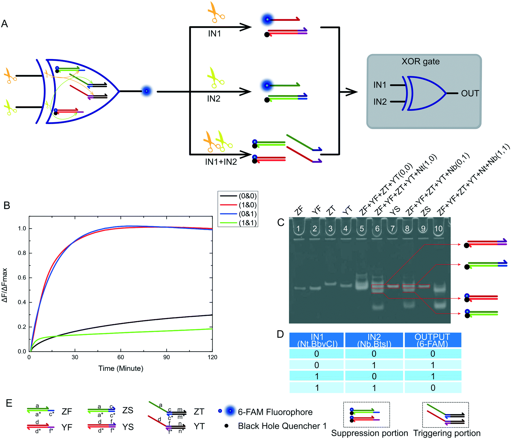 | ||
| Fig. 2 (A) The principle scheme of the XOR logic gate and the corresponding logic circuit. (B) Kinetic characterization of the XOR logic gate. The fluorescence measurement starts at the moment the trigger was mixed with the other substrates in each reaction. The input combination corresponding to each curve is labeled on the right. The fluorescence intensity was collected every minute immediately after addition of the trigger to each solution. The data was normalized to the highest intensity level of the true output sample at 3 hours. The reactions with either single Nt.BbvCI or Nb.BtsI (1 & 0 or 0 & 1) both returned true outputs. The reaction with both Nt.BbvCI and Nb.BtsI (1 & 1) showed no significant fluorescence change, indicating a false output. The reaction with no input (0 & 0) showed a leakage of about 29%, which can be considered a false output. (C) Native PAGE for the XOR logic gate. Lane 1: ZF; lane 2: YF; lane 3: ZG; lane 4: YG; lane 5: ZF, YF, ZG and YG, which was the reaction with input (0 & 0); lane 6: ZF, YF, ZG, YG and Nt, which was the reaction with input (1 & 0); lane 7: reaction product of YS; lane 8: ZF, YF, ZG, YG and Nb, which was the reaction with input (0 & 1); lane 9: reaction product of ZS; lane 10: ZF, YF, ZG, YG, Nt and Nb, which was the reaction with input (1 & 1). (D) Truth table for the XOR logic gates. (E) Names of all substrates and other components of the XOR logic gate. | ||
The XOR gate design and logic operation diagram is shown in Fig. 2A. The two inputs to the logic gate were Nt.BbvCI and Nb.BtsI, as they had the same working environment. The logic gate program was made up of four substrates. Their names and the names of each domain on the DNA strand are shown in Fig. 2E. Depending on their function in the logical system, they were divided into a suppression portion and a triggering portion. The suppression portion was made up of two substrates, ZF and YF, which were labeled with a fluorophore and a quencher. The trigger portion was made up of two other substrates, ZT and YT. The entire operation was performed by both parts. The specific operation process of the XOR logic gate is shown in Fig. 3. The whole reaction process included two catalytic cutting reactions and a final chain replacement reaction. The triggering portion and the suppression portion performed different types of cutting reactions using the nicking enzymes. The catalytic product of the triggering portion could perform final chain replacement reactions with the substrate of the suppression portion, which produced the output. We then considered what would happen if the reaction that occurred in the triggering portion was instantaneous but the suppression portion required a certain amount of time to achieve its inhibitory effect. Thus, we artificially controlled the response time interval between the triggering portion and suppression portion. We also did time interval experiments (see Fig. S3†). From our results, it worked best when the interval was 60 min, but shorter time intervals were also possible. Therefore, the DNA substrates were added sequentially. First the suppression portion was incubated with the input enzymes, and after 60 minutes, the triggering portion was added to the reaction mixture.
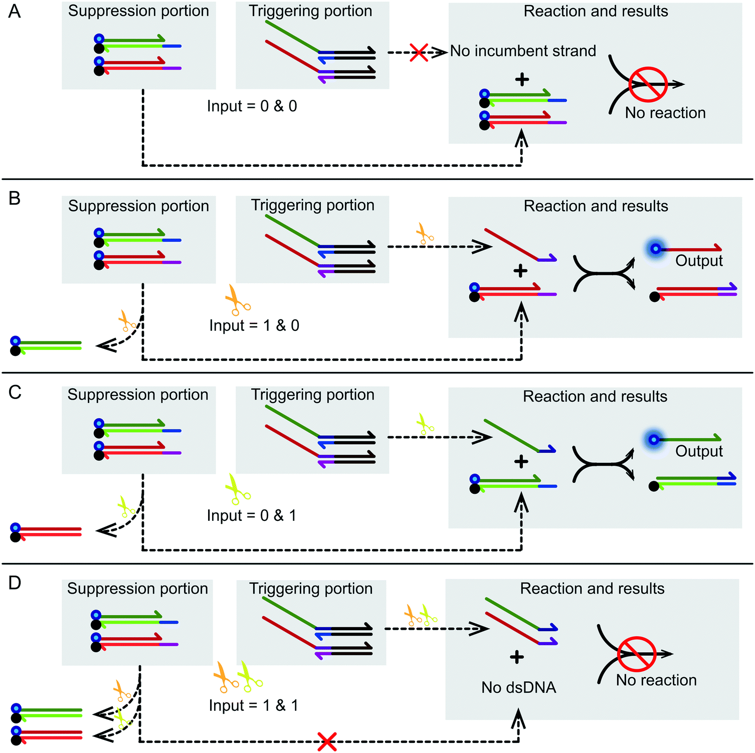 | ||
| Fig. 3 The specific operation process of the XOR logic gate. (A) Reaction process with no input (0 & 0). As there was no incumbent strand, strand displacement did not occur. (B) Reaction process with Nt.BbvCI (1 & 0). The catalyst product of YT reacted with YF, replacing a strand (df) labeled with a 6-FAM fluorophore. The fluorescence intensity changed from low level to high level. (C) Reaction process with Nb.BtsI (0 & 1). The catalyst product of ZT reacted with ZF replacing a strand (ac) labeled with a 6-FAM fluorophore. (D) Reaction process with Nb.BtsI and Nt.BbvCI (1 & 1). In the end, because the two substrates of the suppression portion were restricted by the two nicking enzymes, no reaction occurred. | ||
Fig. 3A shows the logic gate input as (0 & 0), which was the initial state of this logic gate system. There was no addition of any enzyme to the system at this point, only the suppression portion and the triggering portion, which were in their initial states. None of the four substrates were catalyzed, and no catalytic products were produced. Finally, as no strand displacement reaction occurred, no fluorescence was converted from the negative state to the positive state. At this time, the output of the logic system was false. Fig. 3B shows what happens when the logical gate input was (1 & 0). The input to the logical system was only Nt.BbvcI. Under the action of Nt.BbvCI, the substrate ZF of the suppression portion was cut. The toehold domain (c*) was cut off. This meant that substrate ZF lost its potential to participate in subsequent chain replacement reactions. Subsequently, the substrate YT of the trigger portion was cut, releasing an incumbent strand (dfn) that had the potential for chain replacement. As a result, a standard DNA strand replacement reaction occurred. The reaction displaced a strand labeled with a 6-FAM fluorophore, and the fluorescence intensity changed from low to high. The output of the logical system was true. Fig. 3C shows what happens when the logical gate input was (0 & 1), which was almost the mirror image of the (1 & 0) input. The input to the logical system was only Nb.BtsI. In the case of Nb.BtsI, a chain displacement reaction occurred between the substrate ZF and an incumbent strand (acm). A strand (ac) labeled with a 6-FAM fluorophore was thus replaced. The fluorescence intensity of the system changed from low to high, and the output result of the logic system was true. Fig. 3D shows what happens when the logical gate input was (1 & 1). The logical system was affected by both Nt.BbvcI and Nb.BtsI. Both the substrate ZT and YT of the triggering portion were triggered. There were two incumbent strands, (dfn) and (acm). But both substrates ZF and YF of the suppression portion are limited. Thus, there was no expected reaction, and this logic system output false. Kinetic characterization of the XOR logic gate is shown in Fig. 2B, and gel electrophoresis results are shown in Fig. 2C. The products of the two chain replacement reactions, ZS and YS, and the catalyzed substrate were specially labeled and can be clearly seen. Thus, our XOR logic gate was demonstrated to be feasible.
One feature of our design for an XOR logic gate was the introduction of a nicking enzyme as the input of the logic system. Another feature was the transformation of the signal transmission mode. These two seemingly insignificant changes have brought many improvements to our logic gate. The most obvious improvement was the simplification of the logical system structure. The complete XOR logic system consisted of only two parts, containing only a total of four substrates. Logical operations are performed only through two reactions: the cutting reaction and the DNA strand replacement reaction. This meant that the reaction time was shortened and became very easy to control. Logical operations often have superior efficiency and accuracy to other more complex operations. Thus, based on these results, nicking enzyme-based platforms appear to be very useful for the combination of logic gates, and provide convenient tools for designing and implementing half adder and half subtractor gates which will be discussed in detail below.
2.3 AND gate
After the construction an XOR logic gate, we also attempted to build AND and INHIBIT logic gates. These logic gates are important components of half adder and half subtractor gates. The truth table of the designed AND logic gate is shown in Fig. 4D. The logical output was true if and only if both enzyme inputs existed. For our nicking enzyme platform, the two enzymes we input were required to work together, although both enzymes have some triggering effects on their substrates. Without any enzyme, the desired reaction did not occur. An operational schematic diagram of the AND logic gate is shown in Fig. 4A. Our complete AND logic gate consisted of a trigger portion and a suppression portion, with each part having a substrate. Fig. 4E shows the name of the substrate and the names of the domains of the substrate. When designing sequences, we encountered two problems. One was the failure of the recognition site of Nt.BbvCI to use substrate BF (Fig. S4†), which we solved by modifying the sequence of BF (Fig. S5†). Another problem was the problem of substrate BT being accidentally catalyzed by Nt.BbvCI (Fig. S6†), which we solved by modifying the sequence of BT (Fig. S7†). Finally, we finished the design of our AND logic gate. It is important to note that in a reaction involving both enzymes (1 & 1), the red bases on the right side of product BS are not complementary, which was a critical change. More detailed solutions are presented in the ESI.† Gel electrophoresis results are shown in Fig. 4B. Products generated by this reaction can be clearly observed. There was, however, an abnormal phenomenon in the kinetic characteristics, in that the curve was sigmoidal, because the final chain replacement reaction was effected by the cutting efficiency of two nicking enzymes. In addition, the rate was slower than that of the XOR logic gate because we modified the sequence so that the driving force for the final chain displacement reaction decreased. Although the rate was slow, a very good threshold value was displayed within the specified time, indicating that our AND logic gate design was feasible. At 120 minutes, the curves (1 & 1) showed high fluorescence intensity. In fact, the curve continued to rise, flattening out at about 180 minutes. Since a good threshold value was demonstrated, we considered this a feasible experimental result for an AND gate using nicking enzymes.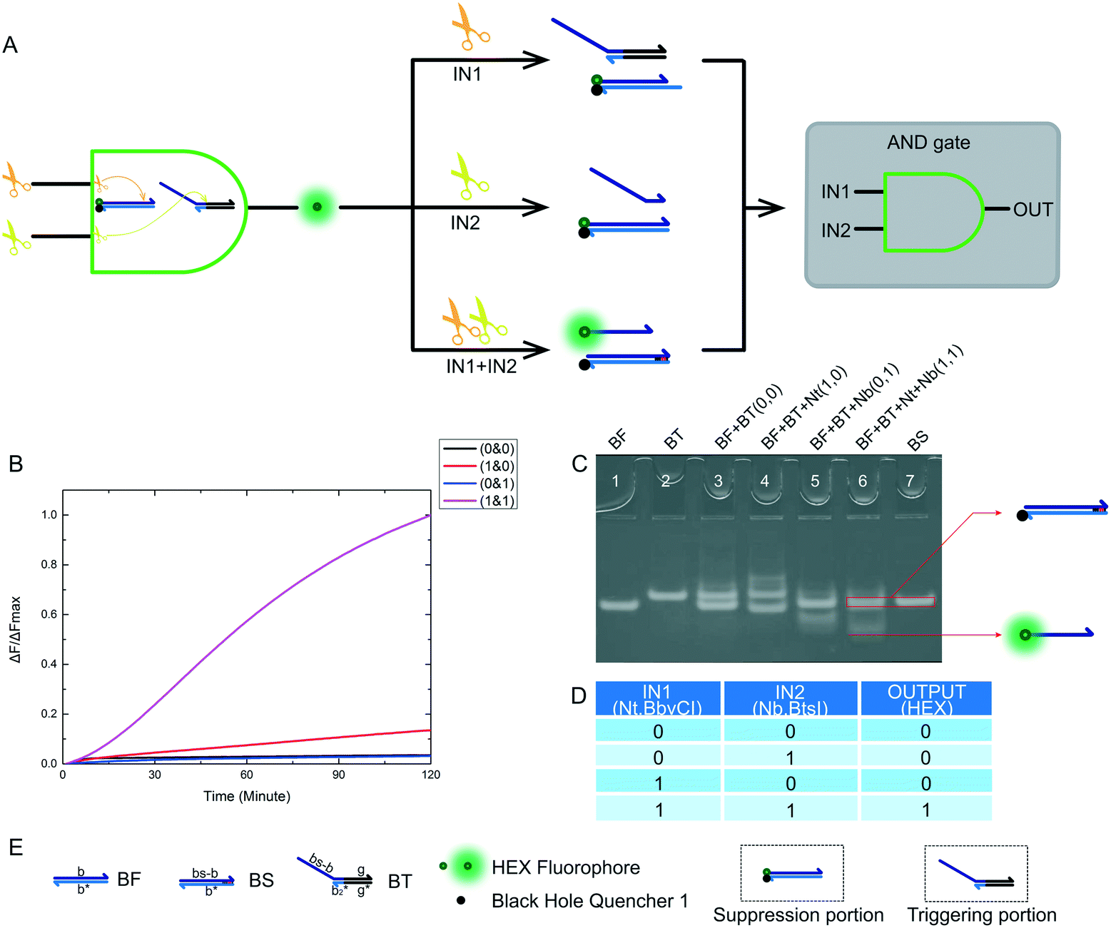 | ||
| Fig. 4 (A) The principle scheme of an AND logic gate and the corresponding logic circuit. (B) Kinetic characterization of an AND logic gate. The fluorescence measurement starts at the moment when the trigger portion is mixed with the other substrates in each reaction. The input combination corresponding to each curve is labeled on the right. The fluorescence intensity was collected every minute immediately after mixing. The data was normalized to the highest intensity level of the true output sample at 3 hours. The reaction with two inputs Nt.BbvCI and Nb.BtsI (1 & 1) showed significant fluorescence change, indicating a true output. The reaction with no input (0 & 0) or a single input of either Nt.BbvCI or Nb.BtsI (1 & 0 or 0 & 1), both showed no significant fluorescence change, which was considered a false output. (C) Native PAGE for the AND logic gate. Lane 1: BF; lane 2: BT; lane 3: BF and BT, which was the reaction with input (0 & 0); lane 4: BF, BT and Nt, which is the reaction with input (1 & 0); lane 5: BF, BT and Nb, which was the reaction with input (0 & 1); lane 6: BF, BT, Nt and Nb, which is was the reaction with input (1 & 1). (D) Truth table for the designed AND logic gate. (E) Names of all substrates and other components of our AND logic gate. | ||
2.4 INHIBIT gate
The INHIBIT logic gate true value table is shown in Fig. 5D. The logical output was true if and only if input 2 itself existed in the reaction. For our nicking enzyme platform, the Nt.BbvCI enzyme was required as an input to inhibit the logic system, and the Nb.BbsI enzyme triggered the logic system. The schematic diagram of our INHIBIT logic gate is shown in Fig. 5A. The input signals were still two different nicking enzymes. This was critical, and it determined whether we had succeeded in building MLDs. The name of the substrate and the name of each domain on the substrate are shown in Fig. 5E. The INHIBIT logic gate structure was as simple as any other logic gate structure we have presented previously, and its experimental results were also excellent. We demonstrated that this INHIBIT logic gate was feasible via fluorescence tracking (Fig. 5B) and PAGE (Fig. 5C).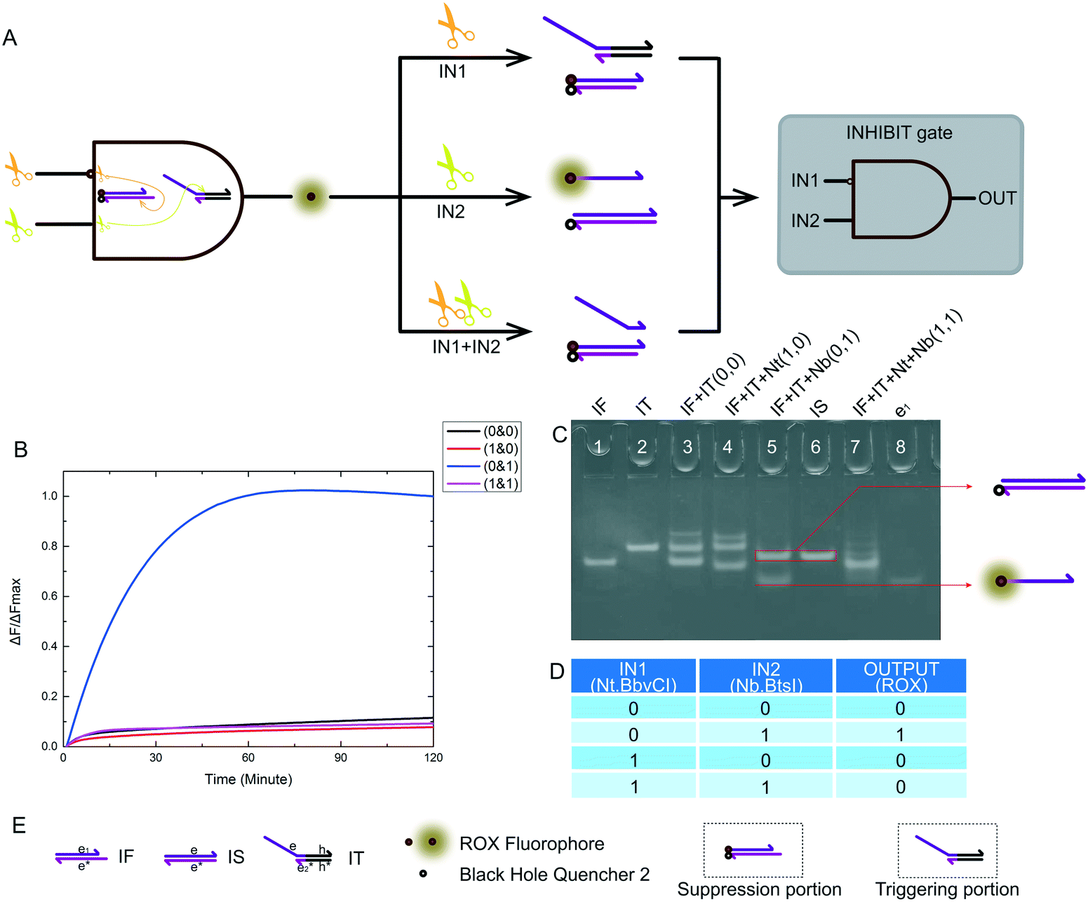 | ||
| Fig. 5 (A) The principle scheme of an INHIBIT logic gate and the corresponding logic circuit. (B) Kinetic characterization of our INHIBIT logic gate. The fluorescence measurement started the moment the trigger portion was mixed with the other substrates in each reaction. The input combination corresponding to each curve is labeled on the right. The fluorescence intensity was collected every minute immediately after mixing. The data was normalized to the highest intensity level of the true output sample at 3 hours. The reaction with only the second input, Nb.BtsI (0 & 1), showed significant fluorescence change, indicating a true output. The reactions with other input situations (0 & 0), (1 & 0) or (1 & 1), showed no significant fluorescence change, and were considered false outputs. (C) Native PAGE for the INHIBIT logic gate. Lane 1: IF; lane 2: IT; lane 3: IF and IT, which was the reaction with input (0 & 0); lane 4: IF, IT and Nt, which was the reaction with input (1 & 0); lane 5: IF, IT and Nb, which was the reaction with input (0 & 1); lane 6: IS; lane 7: IF, IT, Nt and Nb, which was the reaction with input (1 & 1); lane 8: strand e1 (D) truth table for our INHIBIT logic gate. (E) Names of all substrates and other components for our INHIBIT logic gate. | ||
2.5 Half adder
We designed and implemented compatible and combinable logic gates with exactly the same input signals. Combining a XOR logic gate with a AND logic gate is a standard half adder model. The truth table of our half adder combined gate is shown in Fig. 6B. The output of the XOR logic gate was the sum portion of the half adder gate. The output of the AND logic gate was the carry portion of the half adder gate. We mixed the constructed XOR and AND logic gates in the same solution. A half adder based on a nicking enzymes platform was thus constructed. The model and schematic diagram of the half adder gate using nicking enzymes are shown in Fig. 6A. Our complete half adder gate consisted of only six substrates, making it very compact. Fig. 6C–F show the kinetic characterization of this half adder gate. Each diagram illustrates an experiment with a specified combination of inputs. The output of the XOR logic gate (sum) and the AND logic gate (carry) were expressed by the fluorescence variations of FAM and HEX, respectively. The fluorescence intensity of FAM and HEX was unchanged when no enzyme inputs were present. At this point, the calculation result was 0 + 0 = 00 (Fig. 6C). When the input of the half adder operating system was Nt.BbvCI only, the result was 1 + 0 = 01 (Fig. 6D). The calculation of 0 + 1 = 01 was demonstrated when the input of the half adder operating system was only Nb.BtsI (Fig. 6E). When Nt.BbvCI and Nb.BtsI coexisted in the reaction, the XOR gate output was false, and the AND gate output was true, resulting in a calculation of 1 + 1 = 10 (Fig. 6F).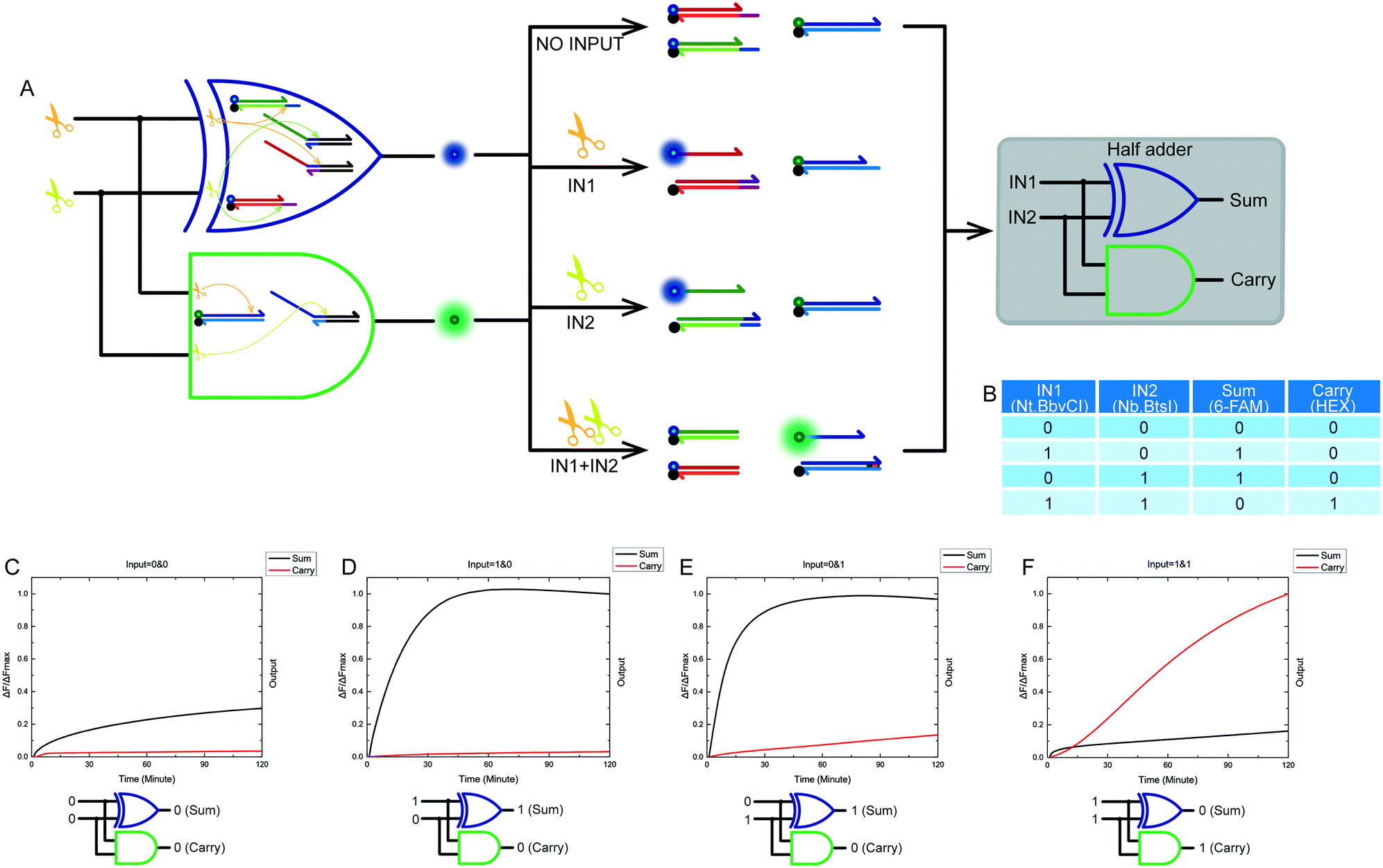 | ||
| Fig. 6 (A) The principle scheme of the designed half adder system and the corresponding logic circuit. (B) Truth table for the half adder system and kinetic characterization of this half adder system (C)–(F). (C) The result of 0 + 0. The carry and sum outputs were both 0, indicating 0 + 0 = 00. (D) The result of 1 + 0. The sum output was 1, and the carry output was 0, indicating 1 + 0 = 01. (E) The result of 0 + 1. The sum output was 1, and the carry output was 0, indicating 0 + 1 = 01. (F) The result of 1 + 1. The sum output was 0, and the carry output was 1, indicating 1 + 1 = 10. The results shown in the four panels correspond to successful operation of a half adder system. The fluorescence intensities of each logic gate were normalized individually. | ||
2.6 Half subtractor
Combining a XOR logic gate with a INHIBIT logic gate is a standard half subtractor model. The truth table for our half subtractor model is shown in Fig. 7B. The output of the XOR logic gate was the difference portion of the half subtractor gate, while the output of the INHIBIT logic gate was the borrow portion. We mixed the constructed XOR logic gate and INHIBIT logic gate in the same solution, resulting in a half subtractor based on a nicking enzymes platform being constructed. The model and schematic diagram of our half subtractor system are shown in Fig. 7A. Our complete half subtractor was as compact as our half adder and consisted of only six substrates. The output of the XOR logic gate (difference) and the INHIBIT logic gate (borrow) were expressed by fluorescence variations of FAM and ROX, respectively. Fig. 7C–F show the kinetic characterization of this half subtractor system. Each diagram illustrates an experiment with a specified combination of inputs. The fluorescence intensity for FAM and ROX were unchanged when no enzyme inputs were present. At this point, the calculation result was 0 − 0 = 00 (Fig. 7C). When the reaction system only had an Nt.BbvCI input, the XOR gate output true, and the INHIBIT gate output false. The calculation result of 1 − 0 = 10 was thus displayed (Fig. 7D). When the reaction system only had Nb.BtsI, the XOR gate output true while the INHIBIT gate output true as well. A calculation result of 0 − 1 = 11 was displayed (Fig. 7E). When the two enzymes coexisted in a reaction, the XOR gate output false and the INHIBIT gate output false, meaning a calculation result of 1 − 1 = 00 was displayed (Fig. 7F).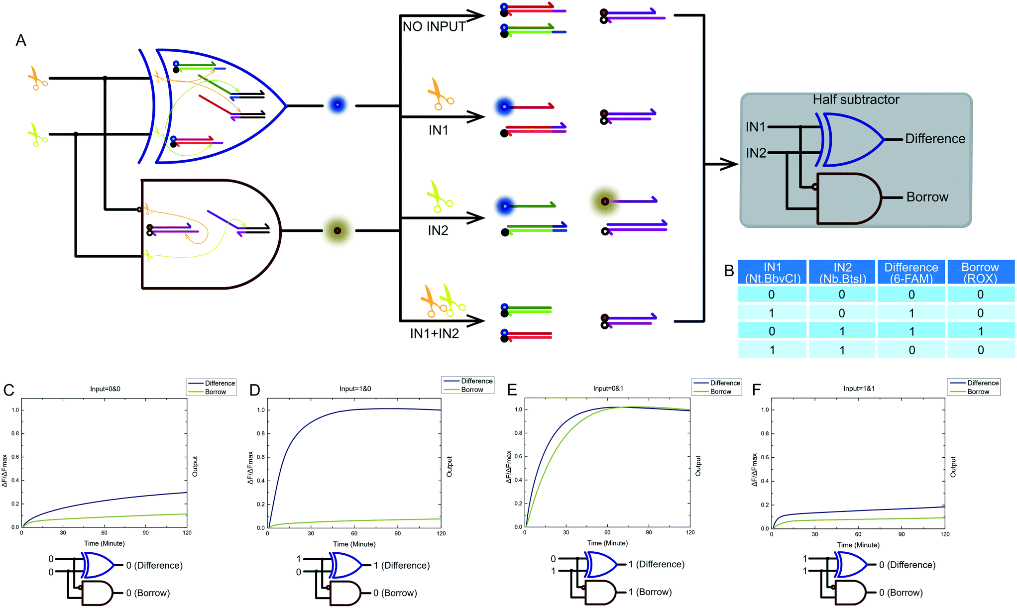 | ||
| Fig. 7 (A) The principle scheme of the designed half subtractor and its corresponding logic circuit. (B) Truth table and kinetic characterization of the designed half subtractor system (C)–(F). (C) The result of 0–0. The difference and borrow outputs were both 0, indicating 0 − 0 = 00. (D) The result of 1 − 0. The difference output was 1, and the borrow output was 0, indicating 1 − 0 = 01. (E) The result of 0 − 1. The difference output was 1, and the borrow output was 1, indicating 0 − 1 = 11. (F) The result of 1 − 1. The difference output was 0, and the borrow output was 0, indicating 1 − 1 = 00. The results shown in the four panels correspond to successful operation of a half subtractor system. The fluorescence intensities of each logic gate were normalized individually. | ||
2.7 Results analysis
One innovation of our logic operating system for molecular devices was that all of the logic operations were implemented on a common nicking enzyme platform. Basic logic gates such as XOR gates, AND gates, INHIBIT gates and more advanced logic devices such as half adders and half subtractors were all built using a universal nicking enzyme platform. Building basic logic gates on the same platform unifies their internal structure so that they all have two-part designs. Combining and using logic gates on the same platform is very convenient, making it is easier to build more advanced logical computing devices. Furthermore, the logic devices used on a single platform have the potential for continued use in combination, thanks to the persistence and compatibility of the nicking enzymes chosen for these experiments.Another breakthrough in the design of logical operating systems for molecular devices presented by this work is that it presents a novel pathway for the transmission of molecular signals. In the past, the internal signal transmission of molecular logic operation equipment was similar to that of traditional electronic logic equipment, meaning it was usually transmitted from upstream to downstream.22 However, due to the limited control technology for biological molecules in a solution, signals cannot be transferred as efficiently as they are in electronic devices. Although parallel computing performance is superior using biological systems, their serial ability is insufficient compared to electronic systems. To combat this, the logic gates constructed using the nicking enzyme platform were designed using two parts. The order of reactions was also changed accordingly. The inhibiting part was catalyzed by the nicking enzyme, leaving a substrate with potential reactivity in this system. The trigger part was then stimulated by an enzyme trigger to produce a chain with the potential to respond. The outcome of the interaction determined the activity of the signal and the potential for subsequent reactions to occur, respectively. During the whole reaction process, the nicking enzyme platform not only triggered the upstream reaction but also assisted the intermediate signal transmission. Thus, it avoided redundant transfer processes and made the efficiency and precision of logical operations using this system excellent and robust.
The use of a nicking enzyme platform and the breakthrough of a novel signal transmission mode have improved the performance of a biological logic operation system. The most obvious improvement was the simplification of the MLD structure. One can see from Fig. 6A and 7A that the half adder and half subtractor systems, based on nicking enzyme platforms, were composed just of 6 dsDNAs, making them very streamlined. Another important improvement was the dramatic reduction in response time. Our results showed that the response time of the fluorescence signal was 120 minutes, and the previous suppression portion response time was 60 minutes, making the total reaction time 180 minutes. In contrast, a half adder based on DNA strand replacement consisting of 13 dsDNAs had a reaction time of 1440 minutes.22 The structural simplification of MLDs and the reduction of the logic operation time both benefit from our platform design, and the improvement of basic logic gates via a two-part design was a key innovation of our nicking platform. In particular, the transformation of biomolecular signal transmission mode greatly simplified the transmission process. It is not hard to see that in our design, the input signal was a set of nicking enzymes. But these nicking enzymes can much more than just serving as input signals in computing systems. If we want to build more complex cascaded logic circuits, nicking enzymes can still be used to assist the logical operations of other logic gates. This requires that cascaded logic gates use not only a set of nicking enzymes as inputs, but also a set of DNA strands as inputs. Our future work will seek to address this. If successful, this should boost the development of serial transmission using biomolecular signals. Finally, our work has effectively improved the operation efficiency of MLDs. Our experimental results show that half adder and half subtractor systems based on nicking enzyme platforms are feasible and be successfully constructed.
3 Conclusions
In summary, we constructed an XOR logic operating system using persistent and compatible nicking enzymes. Furthermore, an AND logic gate and an INHIBIT logic gate were constructed using the same nicking enzyme as the XOR logic gate, and could be combined with an XOR logic gate. Finally, the algorithm process of half adder and half subtractor were realized, based on this nicking enzyme platform. One innovation of this logic operating system for molecular devices was that all logic operations in these systems were implemented on a common nicking enzyme platform. These logic gates use a set of nicking enzymes as inputs rather than a set of DNA strands. Another breakthrough in the design of logical operating systems for molecular devices was based on our changing of the manner in which molecular signals were transmitted. The introduction of a nicking enzyme platform and the breakthrough of signal transmission mode both should simplify the structure of MLDs and shorten the time of logic operation. As half adder and half subtractor systems are both basic arithmetic components, future efforts will be directed at building more sophisticated MLDs based on this nicking enzyme platform. Our work provides a system of great potential for building large-scale arithmetic systems with DNA strands, and this work will greatly expand the field of DNA molecular programming related applications. In addition, looking into the future of molecular computing, the potential applications of logic gates in intelligent detection has been further expanded by our work demonstrating logical changes in fluorescence intensity to detect the presence of nicking enzymes.4 Experimental details
4.1 Native polyacrylamide gel electrophoresis
Polyacrylamide gels (12%) were prepared with 1× TAE buffer. All DNAs used were first denatured by heating at 90 °C for 10 min and then cooled slowly to 25 °C. Each sample (20 μL) was mixed with loading buffer (5 μL) before loading on a gel. Each gel was run at a constant voltage of 70 V over a period of about 80 min. Gels were then immersed in 1× Stains All nucleic acid gel stain solution for about 30 min and then washed twice with water. After gels had been dyed, they were left in natural light to fade until colorless.4.2 Fluorescence kinetics
All spectrofluorometric measurements were performed at 37 °C, using a real-time PCR machine (Agilent, G8830A) equipped with a 96-well fluorescence plate reader. In a typical 25 μL reaction volume, the 1× reaction concentration of substrates was 0.5 μM. The assays were performed in 1× NEB CutSmart buffer. Fluorescence intensity was measured every minute for 120 minutes. Each experiment was repeated three times to ensure reproducibility, and the data was then normalized. In each reaction, the initial intensity was subtracted from the intensity at each time point to calculate the fluorescence intensity change. The fluorescence increase at each time point was then divided by the highest fluorescence increase.4.3 Catalysis of nicking enzymes
The catalysis of nicking enzymes was measured in 1× CutSmart buffer at 37 °C. The catalysis period was 1 hour. For experiments on the persistence of nicking enzymes, the catalysis time was 2 hours. For experiments on the compatibility of nicking enzymes, the catalysis time was 1 hour. For XOR, AND, INHIBIT, half adder and half subtractor investigations, the catalysis time was 2 hours.4.4 Logic operation
All logic operations were performed in 1× CutSmart buffer at 37 °C. The suppression portion of the investigated logic devices were first reacted under the catalysis of nicking enzymes. Then trigger portion was added to the reaction system and the trigger part reacted under the catalysis of nicking enzymes. After catalysis, it took 1 hour for strand displacement. The total reaction time was 3 hours. Sequences for all DNAs used can be found in Table S1 in the ESI.† All the chemicals and materials used can be found in the ESI.†Conflicts of interest
The authors declare no conflict of interest.Acknowledgements
This work is supported by the National Natural Science Foundation of China (No. 61425002, 61751203, 61772100, 61572093, 61672121, 61802040, 61972266), Program for Changjiang Scholars and Innovative Research Team in University (No. IRT_15R07), the Program for Liaoning Innovative Research Team in University (No. LT2017012), the Natural Science Foundation of Liaoning Province (No. 20180551241), the High-level Talent Innovation Support Program of Dalian City (No. 2017RQ060, 2018RQ75), Scientific Research Starting Foundation of Shenyang Aerospace University (18YB38).References
- K. S. Park, M. W. Seo, C. Jung, J. Y. Lee and H. G. Park, Small, 2012, 8, 2203–2212 CrossRef CAS PubMed.
- F. Daoqing, F. Yongchao, W. Erkang and D. Shaojun, Chem. Sci., 2018, 9, 6981–6987 RSC.
- K. Liu, B. Wang, H. Lv, X. Wei and Q. Zhang, IEEE Access, 2019, 7, 88811–88821 Search PubMed.
- P. Ruizi, Z. Xiaofang, L. Yifan, X. Liujun, Z. Xiaobing, K. Guoliang, L. Qiaoling, Y. Changjun, H. Shuangyan and T. Weihong, J. Am. Chem. Soc., 2018, 140, 9793–9796 CrossRef PubMed.
- B. Wang, X. Zheng, S. Zhou, C. Zhou, X. Wei, Q. Zhang and Z. Wei, IEEE/ACM Trans. Comput. Biol. Bioinf., 2018, 15, 999–1002 Search PubMed.
- J. Li, A. A. Green, H. Yan and C. Fan, Nat. Chem., 2017, 9, 1056 CrossRef CAS PubMed.
- X. Zheng, J. Yang, C. Zhou, C. Zhang, Q. Zhang and X. Wei, Nucleic Acids Res., 2018, 47, 1097–1109 CrossRef PubMed.
- Y. Guo, J. Wu and H. Ju, Chem. Sci., 2015, 6, 4318–4323 RSC.
- J. Zhu, L. Zhang, S. Dong and E. Wang, ACS Nano, 2013, 7, 10211–10217 CrossRef CAS PubMed.
- C. Zhang, J. Yang, S. Jiang, Y. Liu and H. Yan, Nano Lett., 2015, 16, 736–741 CrossRef PubMed.
- L. Qian and E. Winfree, Science, 2011, 332, 1196–1201 CrossRef CAS PubMed.
- J. Chen, S. Zhou and J. Wen, Angew. Chem., 2015, 127, 456–460 CrossRef.
- H. Li, W. Hong, S. Dong, Y. Liu and E. Wang, ACS Nano, 2014, 8, 2796–2803 CrossRef CAS PubMed.
- F. Pu, J. Ren and X. Qu, Adv. Mater., 2014, 26, 5742–5757 CrossRef CAS PubMed.
- M. N. Stojanovic, D. Stefanovic and S. Rudchenko, Acc. Chem. Res., 2014, 47, 1845–1852 CrossRef CAS PubMed.
- J. Elbaz, F. Wang, F. Remacle and I. Willner, Nano Lett., 2012, 12, 6049–6054 CrossRef CAS PubMed.
- F. Wang, C.-H. Lu and I. Willner, Chem. Rev., 2014, 114, 2881–2941 CrossRef CAS PubMed.
- D. Y. Tam, Z. Dai, M. S. Chan, L. S. Liu, M. C. Cheung, F. Bolze, C. Tin and P. K. Lo, Angew. Chem., Int. Ed., 2016, 55, 164–168 CrossRef CAS PubMed.
- L. M. Adleman, Science, 1994, 1021–1024 CrossRef CAS PubMed.
- H. Li, S. Guo, Q. Liu, L. Qin, S. Dong, Y. Liu and E. Wang, Adv. Sci., 2015, 2, 1500054 CrossRef PubMed.
- K. Wang, J. Ren, D. Fan, Y. Liu and E. Wang, Chem. Commun., 2014, 50, 14390–14393 RSC.
- W. Li, F. Zhang, H. Yan and Y. Liu, Nanoscale, 2016, 8, 3775–3784 RSC.
- H.-Y. Lin, J.-Z. Chen, H.-Y. Li and C.-N. Yang, Sci. Rep., 2015, 5, 10686 CrossRef CAS PubMed.
- R. Orbach, F. Wang, O. Lioubashevski, R. Levine, F. Remacle and I. Willner, Chem. Sci., 2014, 5, 3381–3387 RSC.
- S. Liu, M. Li, X. Yu, C.-Z. Li and H. Liu, Chem. Commun., 2015, 51, 13185–13188 RSC.
- D. Kang, R. J. White, F. Xia, X. Zuo, A. Vallée-Bélisle and K. W. Plaxco, NPG Asia Mater., 2012, 4, e1 CrossRef.
- D. Fan, J. Zhu, Y. Liu, E. Wang and S. Dong, Nanoscale, 2016, 8, 3834–3840 RSC.
- C. Wu, K. Wang, D. Fan, C. Zhou, Y. Liu and E. Wang, Chem. Commun., 2015, 51, 15940–15943 RSC.
- R. Orbach, B. Willner and I. Willner, Chem. Commun., 2015, 51, 4144–4160 RSC.
- S. Zhang, K. Wang, C. Huang, Z. Li, T. Sun and D.-M. Han, Nanoscale, 2016, 8, 15681–15688 RSC.
- D. Fan, E. Wang and S. Dong, ACS Appl. Mater. Interfaces, 2017, 9, 1322–1330 CrossRef CAS PubMed.
- D. Fan, K. Wang, J. Zhu, Y. Xia, Y. Han, Y. Liu and E. Wang, Chem. Sci., 2015, 6, 1973–1978 RSC.
- J. Zhu, L. Zhang, T. Li, S. Dong and E. Wang, Adv. Mater., 2013, 25, 2440–2444 CrossRef CAS PubMed.
- R. Orbach, S. Lilienthal, M. Klein, R. Levine, F. Remacle and I. Willner, Chem. Sci., 2015, 6, 1288–1292 RSC.
- C.-N. Yang, C.-Y. Hsu and Y.-C. Chuang, Chem. Commun., 2012, 48, 112–114 RSC.
- X. He, Z. Li, M. Chen and N. Ma, Angew. Chem., Int. Ed., 2014, 53, 14447–14450 CrossRef CAS PubMed.
- Y. Wang, J. Sun, X. Zhang and G. Cui, Adv. Sci. Lett., 2011, 4, 383–390 CrossRef CAS.
- S. Zhang, K. Wang, K.-B. Li, F. Chen, W. Shi, W.-P. Jia, J. Zhang and D.-M. Han, Nanoscale, 2017, 9, 11912–11919 RSC.
- X. Zhang, R. Cheng, Z. Shi and Y. Jin, Sens. Actuators, B, 2017, 244, 387–392 CrossRef CAS.
- Y. Yan, S. Yue, T. Zhao, B. Luo and S. Bi, Chem. Commun., 2017, 53, 12201–12204 RSC.
- D. Fan, X. Zhu, S. Dong and E. Wang, ChemPhysChem, 2017, 18, 1767–1772 CrossRef CAS PubMed.
- D. Fan, E. Wang and S. Dong, Nano Res., 2017, 10, 2560–2569 CrossRef CAS.
- X. Lin, Y. Liu, J. Deng, Y. Lyu, P. Qian, Y. Li and S. Wang, Chem. Sci., 2018, 9, 1774–1781 RSC.
- S. Xu, H. Li, Y. Miao, Y. Liu and E. Wang, NPG Asia Mater., 2013, 5, e76 CrossRef CAS.
- J. Ye, G. Coulouris, I. Zaretskaya, I. Cutcutache, S. Rozen and T. L. Madden, BMC Bioinf., 2012, 13, 134 CrossRef CAS PubMed.
- X. Zuo, F. Xia, Y. Xiao and K. W. Plaxco, J. Am. Chem. Soc., 2010, 132, 1816–1818 CrossRef CAS PubMed.
- K. J. Roux, D. I. Kim, M. Raida and B. Burke, J. Cell Biol., 2012, 196, 801–810 CrossRef CAS PubMed.
- J. Bath, S. J. Green and A. J. Turberfield, Angew. Chem., Int. Ed., 2005, 44, 4358–4361 CrossRef CAS PubMed.
- L. Xue, X. Zhou and D. Xing, Anal. Chem., 2012, 84, 3507–3513 CrossRef CAS PubMed.
- E. Kim, S. Kim, D. H. Kim, B.-S. Choi, I.-Y. Choi and J.-S. Kim, Genome Res., 2012, 22, 1327–1333 CrossRef CAS PubMed.
- Z. Luo, Y. Wang, X. Lu, J. Chen, F. Wei, Z. Huang, C. Zhou and Y. Duan, Anal. Chim. Acta, 2017, 984, 177–184 CrossRef CAS PubMed.
- X. Cui, R. Li, X. Liu, J. Wang, X. Leng, X. Song, Q. Pei, Y. Wang, S. Liu and J. Huang, Anal. Chim. Acta, 2018, 997, 1–8 CrossRef CAS PubMed.
- B. Shlyahovsky, D. Li, Y. Weizmann, R. Nowarski, M. Kotler and I. Willner, J. Am. Chem. Soc., 2007, 129, 3814–3815 CrossRef CAS PubMed.
- A. Padirac, T. Fujii, A. EsteÌĄvez-Torres and Y. Rondelez, J. Am. Chem. Soc., 2013, 135, 14586–14592 CrossRef CAS PubMed.
- A. N. Marchi, I. Saaem, J. Tian and T. H. LaBean, ACS Nano, 2013, 7, 903–910 CrossRef CAS PubMed.
- B.-C. Yin, Y.-Q. Liu and B.-C. Ye, Anal. Chem., 2013, 85, 11487–11493 CrossRef CAS PubMed.
- Y. Huang, J. Chen, S. Zhao, M. Shi, Z.-F. Chen and H. Liang, Anal. Chem., 2013, 85, 4423–4430 CrossRef CAS PubMed.
- F. Wang, L. Freage, R. Orbach and I. Willner, Anal. Chem., 2013, 85, 8196–8203 CrossRef CAS PubMed.
- Q. Zhang, F. Chen, F. Xu, Y. Zhao and C. Fan, Anal. Chem., 2014, 86, 8098–8105 CrossRef CAS PubMed.
- Y. Zhao, F. Chen, Q. Zhang, Y. Zhao, X. Zuo and C. Fan, NPG Asia Mater., 2014, 6, e131 CrossRef CAS.
- L. Jin, L. Feng, G. Liu and C. Wang, IEEE Trans. Knowl. Data Eng., 2017, 29, 1508–1521 Search PubMed.
- L. Pan, Z. Wang, Y. Li, F. Xu, Q. Zhang and C. Zhang, Nanoscale, 2017, 9, 18223–18228 RSC.
Footnote |
| † Electronic supplementary information (ESI) available. See DOI: 10.1039/c9me00090a |
| This journal is © The Royal Society of Chemistry 2019 |