
 Open Access Article
 This Open Access Article is licensed under a Creative Commons Attribution-Non Commercial 3.0 Unported Licence
Luminescence thermometry for in situ temperature measurements in microfluidic devices†
Robin G.
Geitenbeek
 *a,
Jeroen C.
Vollenbroek
*b,
Hannah M. H.
Weijgertze
a,
Corentin B. M.
Tregouet
bc,
Anne-Eva
Nieuwelink
d,
Chris L.
Kennedy
e,
Bert M.
Weckhuysen
d,
Detlef
Lohse
c,
Alfons
van Blaaderen
e,
Albert
van den Berg
b,
Mathieu
Odijk
b and
Andries
Meijerink
*a
*a,
Jeroen C.
Vollenbroek
*b,
Hannah M. H.
Weijgertze
a,
Corentin B. M.
Tregouet
bc,
Anne-Eva
Nieuwelink
d,
Chris L.
Kennedy
e,
Bert M.
Weckhuysen
d,
Detlef
Lohse
c,
Alfons
van Blaaderen
e,
Albert
van den Berg
b,
Mathieu
Odijk
b and
Andries
Meijerink
*a
aCondensed Matter and Interfaces, Debye Institute for Nanomaterials Science, Utrecht University, Princetonplein 1, 3584 CC Utrecht, The Netherlands. E-mail: A.Meijerink@uu.nl
bBIOS, the Lab-on-a-Chip group, MESA+ Institute of Nanotechnology, University of Twente, P.O. box 217, Enschede, The Netherlands
cPhysics of Fluids, MESA+ Institute of Nanotechnology, University of Twente, P.O. box 217, Enschede, The Netherlands
dInorganic Chemistry and Catalysis, Debye Institute for Nanomaterials Science, Utrecht University, Princetonplein 1, 3584 CC Utrecht, The Netherlands
eSoft Condensed Matter, Debye Institute for Nanomaterials Science, Utrecht University, Princetonplein 1, 3584 CC Utrecht, The Netherlands
First published on 25th February 2019
Abstract
Temperature control for lab-on-a-chip devices has resulted in the broad applicability of microfluidics to, e.g., polymerase chain reaction (PCR), temperature gradient focusing for electrophoresis, and colloidal particle synthesis. However, currently temperature sensors on microfluidic chips either probe temperatures outside the channel (resistance temperature detector, RTD) or are limited in both the temperature range and sensitivity in the case of organic dyes. In this work, we introduce ratiometric bandshape luminescence thermometry in which thermally coupled levels of Er3+ in NaYF4 nanoparticles are used as a promising method for in situ temperature mapping in microfluidic systems. The results, obtained with three types of microfluidic devices, demonstrate that temperature can be monitored inside a microfluidic channel accurately (0.34 °C) up to at least 120 °C with a spot size of ca. 1 mm using simple fiber optics. Higher spatial resolution can be realized by combining luminescence thermometry with confocal microscopy, resulting in a spot size of ca. 9 μm. Further improvement is anticipated to enhance the spatial resolution and allow for 3D temperature profiling.
Introduction
In the past decades microfluidics rapidly gained interest because of its potential to design compact devices for fast and reliable analysis.1,2 The small quantities of required reagents and produced waste, low cost, short analysis time and ability to carry out separation and detection with high resolution and sensitivity make microfluidic devices ideal for portable analytics. After initial application as analytical systems, the field was expanded to applications in chemical synthesis.3–5 Continuous flow reactions in microfluidic devices can result in faster synthesis at smaller scales with the ability to detect ‘short-lived’ reaction intermediates and to monitor and control reaction kinetics over the course of the microfluidic device.In order to increase the applicability of microfluidic devices, different functionalities can be integrated. One of the most important functionalities in a microfluidic device is temperature control. By monitoring and controlling the temperature distribution and the temperature range, applications such as polymerase chain reaction (PCR),6,7 temperature gradient focusing for electrophoresis8,9 and nanocrystal syntheses10,11 become possible.
External heating methods rely on producing heat outside the microfluidic device and subsequently transferring the heat inside the microfluidic device. This was demonstrated using Peltier elements12,13 or externally heated fluids.14 Integrated heating techniques include exploiting endo- and exothermic processes,15 microwave heating16–19 and Joule heating.20–23 Joule heating has the advantage of fast temperature cycling, steep gradients, and localized heating.24–26 By locating platinum thin film structures in close proximity to microfluidic channels, the channels can be heated efficiently by applying a voltage over the platinum microstructures.27 Dedicated thin film temperature sensor structures of platinum,28 nickel29 or gold30 can be used to measure the temperature of a microfluidic device by exploiting the temperature-dependent resistance of the metal used and are known for their high stability and sensitivity. By monitoring the resistance, temperature read-outs can be achieved in an accurate, reproducible and relatively fast manner. Although the spatial resolution of such a thin film structure can be 30 μm or smaller, monitoring temperature at multiple locations within a microfluidic device requires extensive wiring and electronics and can be limited due to spatial constraints. An additional advantage of Joule heating is that the heater itself can also be used for temperature sensing, although the same spatial constraints remain.
To overcome this localization problem, non-invasive spectroscopic techniques have been developed to monitor temperature at multiple locations within microfluidic devices. The parameters observed in these spectroscopic techniques are, for instance, the luminescence intensity31 or absorbance32 of a dye molecule and the intensity ratio of the Stokes and anti-Stokes peaks in Raman spectroscopy.33 Although the techniques work, there are also several disadvantages. Fluorescent dyes have the disadvantage of being linear in a small temperature range.34–37 Although Rhodamine B, for example, has excellent temperature sensitivity (2.3% K−1),37 it is shown that the sensitivity of Rhodamine B goes down rapidly above 80 °C.34 Therefore, the range of the use of fluorescent dyes is limited. Furthermore, the fluorescence intensity measured with fluorescent dyes is dependent on the concentration, in contrast to a ratiometric technique, which is independent of temperature probe concentration. In Raman spectroscopy, the ratio between Stokes and anti-Stokes peaks are compared, resulting in a ratiometric technique which does not depend on the probe concentration. However, Raman signals are typically very weak and the local environment has a large influence on the Raman signal.
In this work we introduce bandshape luminescence thermometry38,39 as an alternative ratiometric spectroscopic technique to accurately monitor temperature non-invasively. This type of luminescence thermometry exploits the changes in the intensity ratio of two or more emission peaks with temperature.40,41 Here, the lanthanide dopant Er3+ incorporated in NaYF4 nanoparticles (NPs) is used as the emitting ion42,43 and Yb3+ is added for efficient upconversion, a process where multiple low-energy photons are used to excite the sample.44 Lanthanide ions have a partly filled 4fn shell that is shielded by filled outer 5s2 and 5p6 shells. A rich energy level structure arises from interactions between the 4fn electrons and transitions between 4fn levels (f–f transitions) and are characterized by a high efficiency and sharp lines. In Er3+, emission between 500 and 570 nm is due to the transitions from the excited states 2H11/2 and 4S3/2 to the 4I15/2 ground state. The energy difference between the two excited states is ca. 700 cm−1 (or several kT), resulting in thermally coupled levels in which the populations are governed by Boltzmann statistics in a wide temperature range (10–900 K).42,45 The sharp emission lines allow for an accurate determination of the relative intensities and therefore lanthanide-doped materials are widely used for remote temperature sensing.41–43
Here we demonstrate how this ratiometric temperature-dependent luminescence in Yb3+, Er3+ co-doped NPs can be used to monitor temperature in microfluidic devices. The ease of implementation and ratiometric signal read-out make this method more reliable than other in situ probes such as fluorescent dyes, and more versatile than external/static sensors such as RTDs. This makes the NaYF4:Yb,Er upconversion nanoparticles promising as accurate probes for temperature sensing and mapping in microfluidic devices. Here we demonstrate for the first time temperature sensing in microfluidics with upconversion nanoparticles. We showcase three different microfluidic devices with varying continuous phases, reactor compositions and temperature monitoring and heating techniques to demonstrate the versatility of luminescence thermometry. The first case shows a comparison between an integrated platinum resistance temperature detector (RTD) and the luminescence thermometry technique which shows good agreement (average offset around 0.34 °C) over a wide range of temperature up to at least 120 °C. The integrated RTD however was only able to monitor temperature at one specific spot while luminescence thermometry has the potential to accurately monitor temperature anywhere in the silicon/glass microreactor. The second showcase highlights the potential to monitor small temperature fluctuations due to the exothermic reaction of hydrochloric acid and ammonia. Here, NPs coated with SiO2 were dispersed in both liquids and upon mixing, a temperature increase of ca. 15 °C was observed in a polydimethylsiloxane (PDMS)/glass microfluidic device. The final showcase exemplifies an increase in spatial resolution by combining the luminescence measurements with confocal microscopy. Here, a glass/glass microreactor with a set temperature gradient was monitored. A temperature gradient of 20 °C ranging from 60 to 40 °C over 500 μm was monitored with a spatial resolution of 9 μm.
These three examples show the great potential for bandshape luminescence thermometry to monitor temperatures within the channels of microfluidic devices. Using this non-invasive technique, temperatures up to at least 120 °C can be monitored with high accuracy (0.34 °C) and great spatial resolution (9 μm) with the potential for 3D temperature mapping.
Methods
Temperature-dependent luminescence
To showcase the potential for luminescence thermometry in microfluidic devices, three different microfluidic devices were prepared and investigated. In all three setups, NaYF4 NPs doped with 18% Yb3+ and 2% Er3+ (indicated as NaYF4 NPs or NPs below) were used as temperature probes. These upconversion NPs are well known for remote temperature sensing.41–43 TEM images of the NPs (ca. 25 nm) are shown in Fig. 1a–c. In the second example (Fig. 1b), the NaYF4 NPs were overgrown with a protective layer of SiO2 (thickness is ca. 10 nm) for chemical stability and dispersibility in polar solvents.42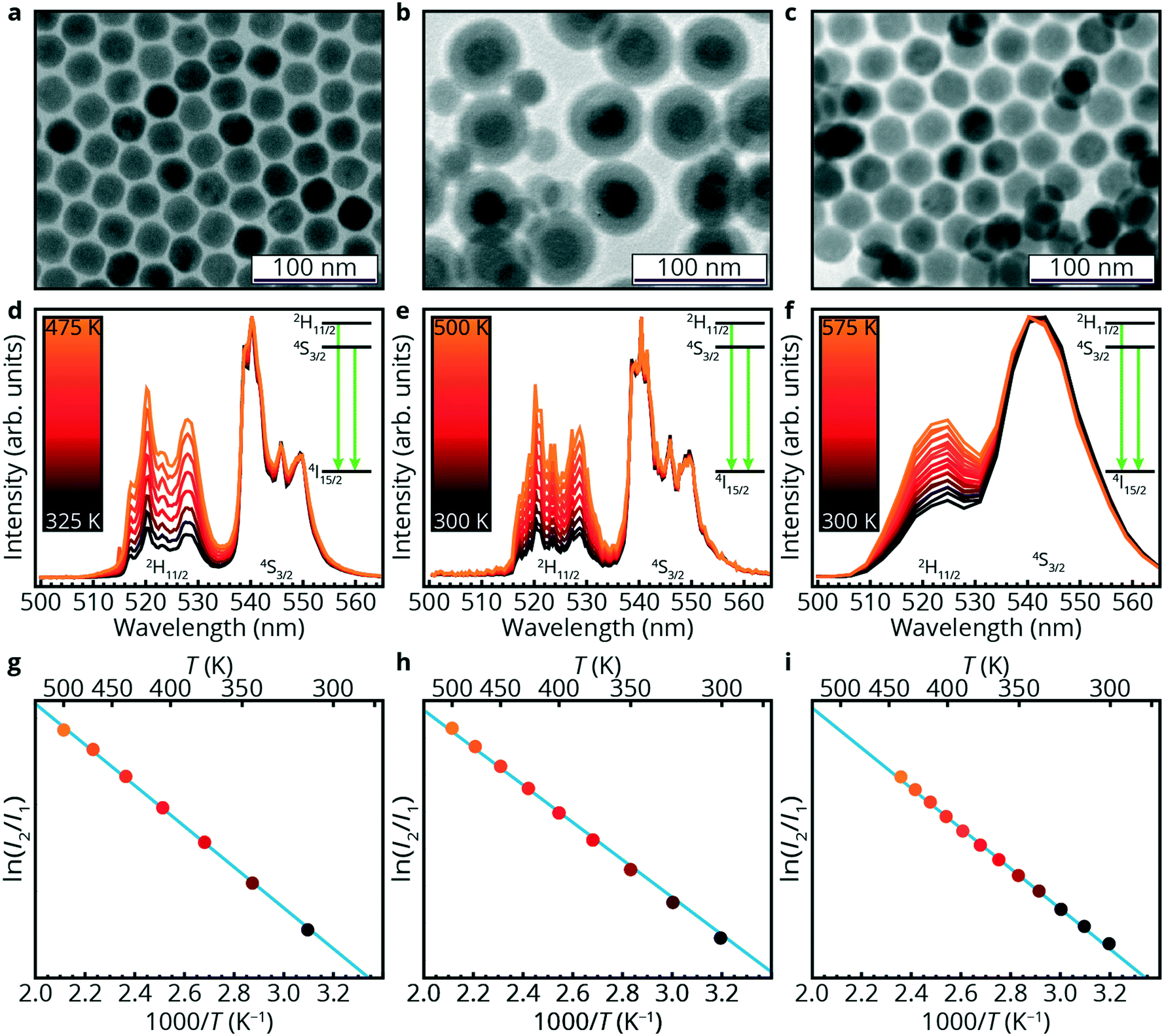 | ||
| Fig. 1 Luminescence and structural characterization. TEM micrographs of NaYF4:Er,Yb NPs (a and c) and NaYF4:Er,Yb@SiO2 NPs (b). Temperature-dependent luminescence of Er3+ doped NaYF4 NPs used for the different temperature sensing experiments in the microfluidic devices discussed in this article (d–f). The inset shows the energy levels from which luminescence is observed. The obtained calibration lines by plotting the natural logarithm of the fluorescence intensity ratio, ln(I2/I1), vs. reciprocal temperature, 1/T (g–i). | ||
In all cases, the NPs showed typical temperature-dependent luminescence as shown in Fig. 1d–f. The similar luminescence of the core/shell NPs compared to the core only NPs shows that the SiO2 does not affect the temperature-dependent luminescence, as expected for the isolated f–f transitions of the lanthanides. Emission spectra were recorded under infrared (980 nm) excitation in Yb3+. Efficient upconversion in the Yb–Er couple gives rise to green emission from Er3+.46,47 At room temperature (black spectra) both emission peaks from the 2H11/2 (525 nm, I2) and 4S3/2 (545 nm, I1) excited states are observed. The small energy difference between the two excited states, ca. 700 cm−1 (several kT at room temperature), guarantees quick relaxation between the two excited states and the population distribution is governed by Boltzmann statistics. Upon increasing temperature (black to orange) the additional thermal energy shifts the population distribution and the emission from the higher excited state, 2H11/2, becomes more intense at the expense of the 4S3/2 emission.40 Based on Boltzmann statistics, the correlation between the natural logarithm of the fluorescence intensity ratio ln(I2/I1) and reciprocal temperature is linear. The linear fits (blue lines) for the three different NPs are shown in Fig. 1g–i. The fits give relative sensitivities42 of 1.12% K−1 for Fig. 1d and e and 0.9% K−1 for Fig. 1f. The fits are of high quality (r2 = 0.999, 0.997 and 0.998, respectively).
Luminescence thermometry on silicon/glass chips
The first experiment to showcase the potential of luminescence thermometry for temperature sensing in microfluidic devices is performed in the glass/silicon chip shown in Fig. 3a–e, k using the fiber optics setup shown in Fig. 2a. Here, the microfluidic device contains integrated platinum heaters and two platinum temperature sensors (TS1 and TS2), as shown in Fig. 3b, d and e. The chip, containing channels with a height of 150 μm and a width of 200 μm, can be used for either continuous (single-phase) flow or droplet flow experiments due to the flow focusing geometry. During the experiments a single-phase continuous flow of 50 μL min−1 was used. Three experiments were performed where the temperature was cycled from 70 °C to 120 °C and back. Between the heating and cooling, sufficient time was taken for the temperature to stabilize. For heating up this was 5–10 s between the steps, and for cooling down this was sometimes 30 s or more, because the chip was not actively cooled. The temperature was monitored using both the integrated platinum temperature sensors and the NaYF4 NPs (Fig. 1a) dispersed in 1-octadecene (ODE). First, the output from the two types of sensors was compared by monitoring temperatures using both the integrated temperature sensor TS2 and the luminescence output at the same location. Subsequently, another temperature measurement at a second spot further away from TS2 was measured using luminescence thermometry and compared with TS2. The yellow circles in Fig. 3a and b indicate the measurement spots for luminescence thermometry.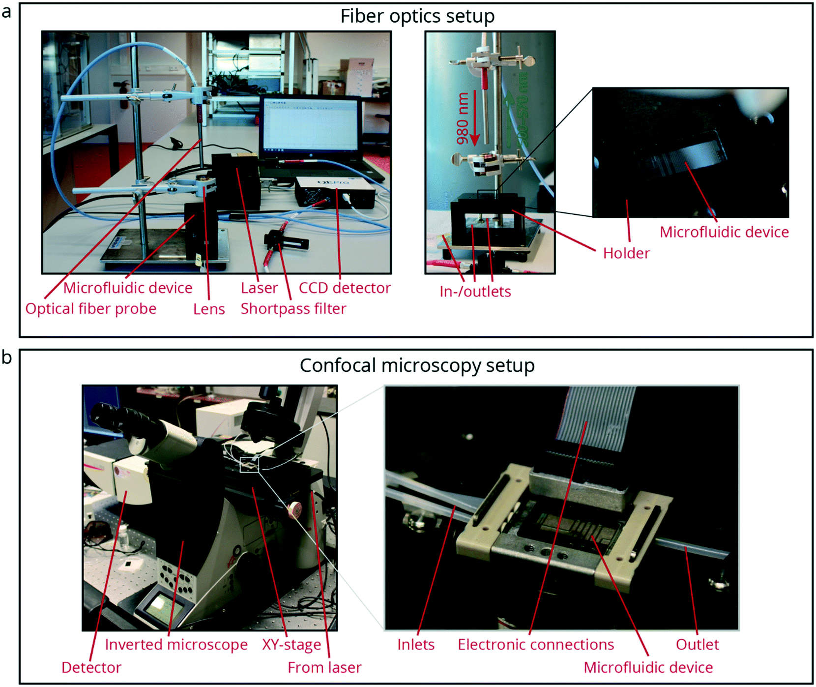 | ||
| Fig. 2 Overview of the spectroscopy setups used. An optical fiber probe excited the NPs within the microfluidic device using a 980 nm laser coupled into the fiber using a collimator. The light is focused using a lens and afterwards, the light is collected with the sample fiber probe. The collected light is monitored with a CCD detector after passing through a short pass filter (a). For higher resolutions, the inverted confocal microscopy setup is used, where a sample is mounted on an XY-stage to allow for optical measurements at different spots on the microfluidic device (b). | ||
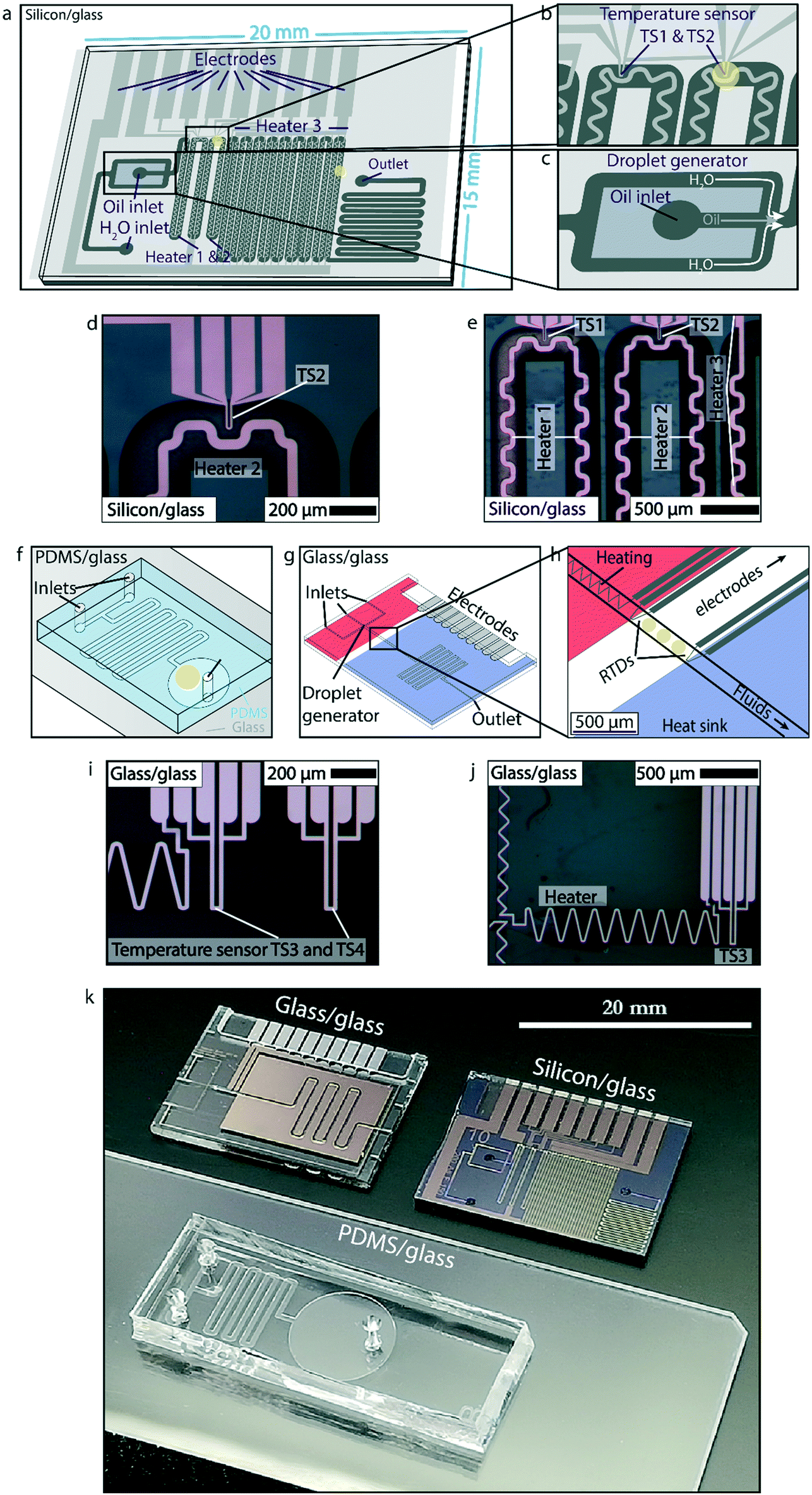 | ||
| Fig. 3 Schematic overview of the microfluidic devices used. Droplet-flow silicon/glass chip for on-chip heating and temperature sensing (a). Heating is done using built-in platinum heaters and the temperature is monitored by two built-in platinum temperature sensors TS1 and TS2 (b). Droplets are created by using oil and water inlets and a flow-focusing geometry (c). Droplets subsequently flow through the chip with channels which are 150 μm high and 200 μm wide. Optical microscopy images of TS1, TS2 and the heaters of the silicon/glass chip are shown in (d) and (e). The PDMS/glass chip (f) shows the two inlets and the T-junction, where the acid and base can mix. Channels in the PDMS/glass chip are 50 μm high and 400 μm wide. A schematic overview of the glass/glass chip, including the inlets and outlet, the droplet generator and the electrodes for integrated heating and temperature sensing (g). A zoom-in of the temperature gradient in the chip by exploiting a heat sink and platinum wires for both heating and temperature sensing (h). Channels have a height of 100 μm and are 300 μm wide. Optical microscopy images of TS3, TS4 and the heaters of the glass/glass chip are shown in (i) and (j). Finally, a photograph (k) shows the three microfluidic chips used, the glass/glass chip (top left), silicon/glass chip (top right), and PDMS/glass chip (bottom). Yellow circles indicate the measurement spots in the different chips. | ||
Luminescence thermometry in PDMS/glass chips
In the second showcase, the potential of luminescence thermometry to monitor temperature changes resulting from an exothermic chemical reaction is demonstrated using the fiber optics setup shown in Fig. 2a. In these experiments, NaYF4 NPs are encapsulated in a protective SiO2 shell (Fig. 1b) and afterwards transferred to a 5 M NH3 solution and a 4 M HCl solution, both containing thymol blue. These two solutions are then introduced to a simple PDMS/glass chip with a T-junction where the solutions meet and subsequently meander through the channels (50 μm high and 400 μm wide) of the device as shown in Fig. 3f and k. Experiments were performed at flow rates of 150 μL min−1 under continuous flow conditions. At the end of the meandering chip, the liquid is collected in a large chamber (Fig. 3f and k). The temperature-dependent luminescence of the NaYF4 NPs dispersed in both liquids is monitored at the end of the meandering channels, as indicated by the yellow circle in Fig. 3f. Using the calibration line from Fig. 1h, the spectral output is converted to temperature.Luminescence thermometry in glass/glass chips
The final showcase to highlight the potential of luminescence thermometry in microfluidics involves a microfluidic device (channels are 100 μm high and 300 μm wide) in which a temperature gradient is established by integrated platinum heaters and a heat sink as shown in Fig. 3g–j using the high-resolution microscope setup shown in Fig. 2b. The temperature gradient depends on the settings of the heater and the optional use of an external Peltier element for active cooling (not used in this case), and results in a temperature decrease of ca. 10–20 °C over a distance of 500 μm. The chip is designed to have a stable temperature gradient over a short distance. Using the RTDs (TS3 and TS4 in Fig. 3i), the temperature can be measured over time at two points, separated by 500 μm, to know the gradient. The temperature gradient reaches a steady state in about 5 s and remains constant over more than 1 hour, as shown in Fig. S1.† A variation of 2 to 3 °C has been observed due to varying between flow off and flow on conditions, as shown in Fig. S2.†Although measuring temperature with two RTD sensors can locally give accurate results, two data points are still insufficient to characterize a temperature gradient properly.
In order to obtain better insight into the temperature distribution in the microfluidic channel, NaYF4 NPs (Fig. 1c) dispersed in cyclohexane were flushed through the microfluidic device. Information on the temperature distribution was obtained by monitoring the temperature-dependent luminescence using confocal microscopy while heating the channel, under stagnant flow conditions. By applying a potential of 25 V to the platinum heaters, the chip was heated to 60 °C. The integration of the microfluidic device with confocal luminescence measurements is described in detail in the ESI.† In this fashion, it was possible to probe the temperature at multiple spots of ca. 9 μm to reconstruct the temperature gradient along the channel.
Experimental setup
Setup
Luminescence measurements using the fiber probe were performed using an MDL-III-980 nm-500 mW laser. Upon excitation, light was collected via a fiber patch chord and a shortpass filter to the OceanOptics QEPro CCD detector. Higher spatial resolution was obtained by recording spectra at various positions on the heated chip using a Leica SP8 confocal microscope equipped with a calibrated stage and an infrared laser (Coherent Chameleon II, Ti:Sapphire) tuned to 980 nm. At each position a spectrum was recorded of the emission from a 9 μm × 9 μm field of view obtained via a 40×/0.55 air objective lens. At the spectral resolution limit of the instrument, intensity was measured within a 5 nm spectral window at intervals of 3 nm with an integration time of 2.6 s at each wavelength. With this microscope, spectra were obtained by scanning a 16 × 16 pixel raster across the field of view and recording the intensity within the spectral window at each pixel. To obtain a single value for each wavelength point, and improve SNR, these pixel intensities were integrated. Images of both setups are shown in Fig. 2.NP synthesis
NaYF4@SiO2 nanoparticles (NPs) doped with 18% Yb3+ and 2% Er3+ of ca. 50 nm were prepared via an initial synthesis of NaYF4 core particles (ca. 25 nm) and subsequent SiO2 overgrowth as reported earlier.42,48Silicon/glass chip fabrication
The microreactor is fabricated in the clean room of the MESA+ Nanolab at the University of Twente, as described previously.49 In short, the reactor consists of a silicon and MEMpax (borosilicate glass) substrate anodically bonded together. Fluidic channels are etched into the silicon substrate by deep reactive ion etching (DRIE). A 200 nm SiO2 layer is thermally grown onto walls of the channels by dry oxidation of the silicon substrate.Channels are 150 μm deep and vary from 150 to 300 μm in depth. Buffered HF is used to wet etch small trenches (200 nm) into the MEMpax substrate into which a 10 nm tantalum adhesion layer and 190 nm platinum is sputtered. Subsequently, the Ta/Pt electrodes are covered with 1 μm of SiO2via plasma-enhanced chemical vapor deposition to insulate them from the channels.
PDMS/glass chip fabrication
For fabrication of the PDMS/glass chips a mold out of SU-8, a commonly used epoxy-based photoresist, is made in the MESA+ Nanolab at the University of Twente. Using photolithograpy, SU-8 structures of 100 μm high and 200 μm wide are fabricated on a silicon substrate. After development these structures are used as a soft lithography mold for casting PDMS. A PDMS vs. curing agent mass ratio of 10![[thin space (1/6-em)]](https://www.rsc.org/images/entities/char_2009.gif) :1 is used. The PDMS is then poured on the silicon/SU-8 mold after which it is cured in an oven for two hours at 60 °C. After curing, in- and outlets of 1 mm are punched in the PDMS chip; subsequently the PDMS is treated in an O2 plasma oven for 2 minutes after which it is bonded to a glass substrate. Finally the PDMS/glass chip is heated to 60 °C for 30 minutes to ensure proper bonding.
:1 is used. The PDMS is then poured on the silicon/SU-8 mold after which it is cured in an oven for two hours at 60 °C. After curing, in- and outlets of 1 mm are punched in the PDMS chip; subsequently the PDMS is treated in an O2 plasma oven for 2 minutes after which it is bonded to a glass substrate. Finally the PDMS/glass chip is heated to 60 °C for 30 minutes to ensure proper bonding.
Glass/glass chip fabrication
The microreactor is fabricated in the clean room of the MESA+ Nanolab at the University of Twente. The chip consists of two wafers of borosilicate glass on top of each other. Semi-circular channels are etched with HF in the top wafer: a protective layer of resin (1.7 μm of Olin photoresist) is spin-coated and patterned on the wafer to define the channels (100 μm high and 300 μm wide). On the top wafer, buffered HF is used to wet etch small trenches (100 nm) into the borosilicate wafer into which a 10 nm tantalum adhesion layer and 90 nm platinum is deposited by means of sputtering. Finally, 1 μm of silicon dioxide is grown on top of the electrodes via plasma-enhanced chemical vapor deposition (except on the connecting pads) to electrically isolate the electrodes from the liquids flowing in the channels. Holes are made in the top wafer by powder blasting to access the connecting pads and the two wafers and bonded together at high temperature (625 °C), and finally diced into individual microfluidic chips. The channels cross the dicing lines to provide complete opening of the side inlets and outlets.Results and discussion
Luminescence thermometry on silicon/glass chips
Fig. 4a shows the temperatures as determined with both techniques (platinum RTD and luminescence thermometry) by cycling the temperature between 70 and 120 °C three times on one chip. The red diamonds are the temperatures measured with the integrated Pt thermometers while the cyan dots represent the temperatures calculated from the temperature-dependent luminescence of the NPs.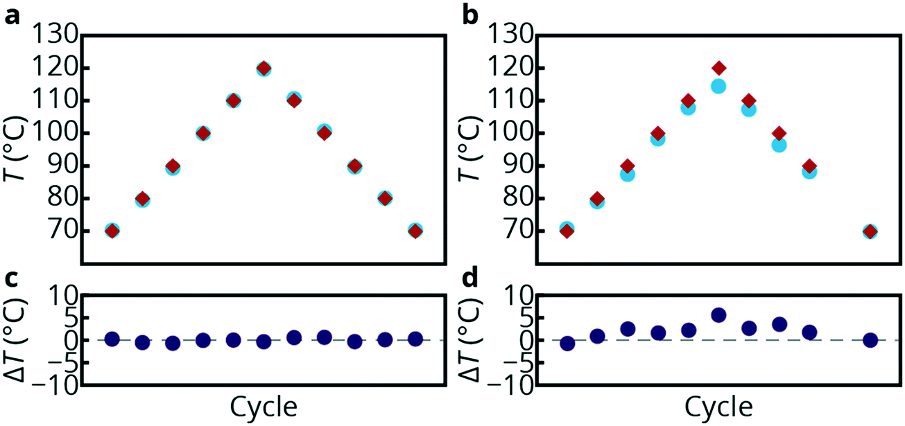 | ||
| Fig. 4 Temperature measurements on silicon/glass chip. Temperature measurements using the on-chip RTD sensors (red diamonds) and temperature-dependent luminescence from the NaYF4 NPs (cyan dots). The temperatures were determined on the same spot as the platinum sensor TS2 (a) and at the end of the chip (b), as indicated by the yellow circles in Fig. 3a and b. The temperature difference measured between the platinum sensor TS2 and the NPs is plotted for the same spot (c) and the end of the chip (d). | ||
The temperature outputs from both techniques are plotted in Fig. 4a and coincide within 0.34 °C on average when measured close to TS2, marked by the left yellow circle in Fig. 3b. The maximum and mean discrepancies observed were 0.68 °C and 0.34 °C, respectively. These results show that the use of thermal resistance detectors is a valid method to monitor temperatures inside microfluidic channels even though the platinum sensors are located 1 μm (separated by a SiO2 layer) above the channels.
Fig. 4b shows the results obtained from both the RTD and the luminescent NPs while monitoring the luminescence output at the outlet of the microfluidic device, as indicated by the rightmost yellow circle in Fig. 3a. Note that only heaters 1 and 2 are switched on during these experiments. The temperatures obtained from the integrated temperature sensors (TS1 and TS2) were measured upon cycling three times from 70 to 120 °C, similar to the previous experiment. However, since the luminescence output is monitored at a different spot in the chip, cooling of the liquid passing through the device can result in lower temperatures monitored with luminescence thermometry. This is indeed observed in Fig. 4b where significant temperature differences are present between the temperatures from the two different temperature sensing techniques. At 70 °C this effect is still minimal; however, at higher temperatures the temperature offset increases, up to a difference of 5.6 °C at 120 °C between the RTD and the luminescent NPs. Although the temperature difference is relatively small as a result of the high thermal conductance of silicon (compared to glass and PDMS), the luminescence thermometry technique is accurate enough to monitor these temperature differences at different positions on the microfluidic device. The experiments show very good agreement (differences less than 0.68 °C) between the different temperature sensors (NPs vs. RTDs). Even though the platinum sensors are just outside the channels, the temperatures obtained from the resistance measurements are representative of temperatures inside the microchannels. However, the fabrication of integrated platinum temperature sensors requires additional production steps such as lithography, sputtering and lift-off. Furthermore, RTDs take up more space on the chip and information on temperature is limited to a local heating area and on the whole microfluidic device to a fixed (small) number of spots. The luminescence thermometry technique shows great potential for accurate monitoring of temperatures inside microfluidic devices by using a non-invasive spectroscopy technique, which can map temperatures at any location on the chip.
Luminescence thermometry in PDMS/glass chips
To further highlight the versatility of luminescence thermometry for T-sensing in microfluidics, a second example is shown below with a PDMS/glass chip that can be used for chemical reactions between reactants that are fed into two channels merging into one channel. Fig. 5a and b show the microfluidic device where 5 M NH3 and 4 M HCl solutions are introduced. The temperature is measured at the end of the microchannel in which the reaction takes place (yellow spot, Fig. 5a). There is an increase in temperature of ca. 15 °C, as shown in Fig. 5c, under continuous flow conditions when the NH3 and HCl solution are mixed. This indicates that the temperature increase due to the exothermicity of the reaction can be monitored. After switching off the flow, the temperature slowly decreases to room temperature.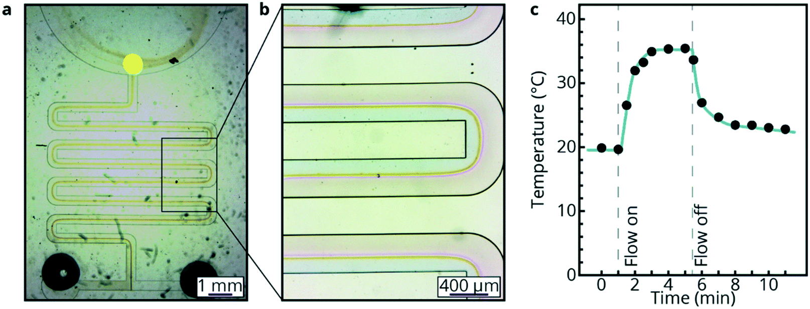 | ||
| Fig. 5 PDMS microfluidic device. Optical microscopy image of a simple microfluidic device (a) with two inlets in which concentrated ammonia (5 M) and hydrochloric acid (4 M) are introduced in combination with a pH indicator, thymol blue. The limited mixing is visualized with the indicator having the red color at low pH, yellow color at intermediate pH and blue color at high pH (b). Temperature measurements which show the rise in temperature due to the exothermic reaction between ammonia and hydrochloric acid (c). The yellow circle in (a) indicates the spot used for temperature sensing using luminescence thermometry with NaYF4 NPs added to both solutions. | ||
The experiments show a clear increase in temperature due to the reaction between the NH3 and HCl solutions. The increase in temperature could probably be higher since the mixing of the two liquids is not efficient due to the laminar flow inside the microfluidic device. This non-efficient mixing probably explains why the steady-state temperature varies between repeated experiments on the same chip. To validate this theory and investigate the mixing behaviour, a pH indicator, thymol blue, was added to both liquids while flowing through the device at a flow rate of 150 μL min−1. Thymol blue has a blue color in alkaline medium (pH 8.0–9.6), a red color in acidic medium (pH = 1.2–2.8) and a yellow color at neutral pH. Images of the thymol blue flowing through the microfluidic device are shown in Fig. 5a and b. It can be observed that the main volume of the liquid is still unmixed (red and blue) while some mixing occurs at the interface (yellow). Due to incomplete mixing, the release of heat by the reaction limits the increase of temperature to ca. 15 °C, as further explained in the ESI.†
Luminescence thermometry in glass/glass chips
To realize higher spatial resolutions, confocal luminescence spectroscopy can be used to measure emission spectra of the luminescent temperature. A glass/glass chip with a steep temperature gradient between a heated part and heat sink, as shown in Fig. 6a, was used for high spatial resolution temperature measurements. The NPs were dispersed in cyclohexane and were subsequently introduced in the microchannels. The NPs showed some clustering as can be observed in Fig. 6b where the black dots are NaYF4 NPs aggregated at the bottom of the microchannel. Emission spectra from the NPs were measured with a confocal microscope and used to map the temperature gradient. The precise location of the measurement points is indicated by the yellow dots in Fig. 6b. Temperatures were calculated from the obtained spectra and a temperature distribution was found as shown in Fig. 6c. Here, the obtained temperatures are plotted vs. the position in the microchannel. A voltage was applied, resulting in a temperature of 60 °C upstream and 40 °C downstream as monitored with the RTDs (TS3 and TS4 from Fig. 3i). The temperatures, measured with the NPs, show a decrease from ca. 60 °C to 40 °C. This is further visualized in Fig. 6d, in which the red color represents 60 °C and the blue color represents 40 °C. The increase in spatial resolution comes with the price of reduced sensitivity: reducing the measured area leads to a smaller number of luminescent NPs in view and thus fewer photons for the analysis, which decreases the signal-to-noise ratio. Because of this, the temperatures found fluctuate around the trend line with a mean difference of 3.6 °C between data points and the linear fit. Although the difference between both measurement techniques is still relatively high, the trend of the temperature gradient can be observed with the luminescent NPs. This is not possible with the RTD present on the chip. Improvement of the signal-to-noise ratio is possible by using a more sensitive CCD detector (instead of a scanning monochromator used here) and by increasing the size of the luminescent NPs. The size of the presently used NPs of ∼20 nm is clearly not the limiting factor for spatial resolution, and as the number of emitters (Er3+ ions) increases with the third power of particle diameter, larger particles will give a stronger signal. Also, improving the upconversion efficiency50 will aid to improve the spatial resolution. It is expected that a spatial resolution down to the diffraction limit or even below can be achieved.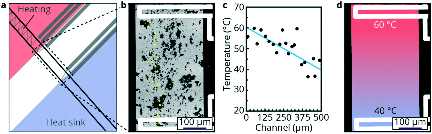 | ||
| Fig. 6 Confocal microscopy on temperature gradient. A schematic representation of the channel area that is designed with the temperature gradient (a). A confocal reflection microscopy image of the area between the two RTDs in white. Specific regions of interest (ROIs) for T-sensing are shown as yellow circles. The NaYF4 NPs are visible as black dots (b). The temperature gradient in a plot of the obtained temperatures from the different ROIs vs. distance from the heating element (c). Visual representation of the temperature gradient in the channel as shown by the cyan line in (c) (d). | ||
The three different showcases demonstrate the versatility and robustness of the luminescence thermometry technique for monitoring temperature within microfluidic devices. By dispersing NPs in the fluids, non-invasive luminescence techniques can be exploited to monitor temperatures within silicon/glass, glass/glass or PDMS/glass microfluidic devices with high accuracy (0.34 °C) up to at least 120 °C and with high spatial resolution.
The approach based on the use of lanthanide-doped inorganic NPs for temperature sensing has multiple advantages. The narrow line f–f emission from different close spaced energy levels of Ln3+ ions allows for accurate remote luminescence temperature sensing. It is shown here that the temperature probes can be used in both polar and apolar solvents by changing the surface of the NPs. The surface chemistry of NPs is well investigated51,52 and offers great flexibility and new opportunities, for instance, to attach the NPs to the inner channel wall of the microfluidic chip as fixed local temperature probes. The inorganic host is inert and the f–f emission of the lanthanide dopants are not influenced by the environment which ensures non-invasive temperature sensing that can be universally applied without the need for calibration. In the presently used NPs, IR excitation of 980 nm is used to induce upconversion, resulting in temperature-dependent luminescence in the visible region. This ensures minimal background fluorescence and thus a superior signal-to-noise ratio. Care has to be taken to verify that the IR excitation does not give rise to sample heating.
The showcases discussed demonstrate that temperature sensing and mapping with lanthanide-doped NPs is possible in three different types of microfluidic devices with different spatial resolutions. For simple cases in which the spatial resolution is required for different discrete regions on the microfluidic device, fiber optics are sufficient to localize excitation and detection of light to the mm regime, allowing one to monitor temperatures at different positions in single channels. If a higher spatial resolution is required, confocal microscopy can be used to reach higher spatial resolutions, down to 9 μm in this work, and with a potential for sub-μm resolution. Confocal microscopy also offers possibilities for high-resolution 3D mapping of temperature profiles.
Conclusions
We have investigated the potential for luminescence thermometry in microfluidic devices using lanthanide-doped NPs. NaYF4 and NaYF4@SiO2 core/shell NPs doped with Er3+ and Yb3+ were used and the temperature-dependent upconversion luminescence of the Er3+ has been exploited for remote temperature sensing by monitoring the spectral output. The as-synthesized NaYF4 NPs were dispersed in apolar solvents. After growing a SiO2 shell the NPs could be transferred to polar media, which gives flexibility in choice of solvents. Due to the ratiometric nature of the technique, the measurements are independent of probe concentration and the use of upconversion luminescence ensures minimal background fluorescence.To showcase the potential of bandshape luminescence thermometry, the temperature inside three different microfluidic devices was monitored. The microfluidic devices were made of silicon/glass, PDMS/glass or glass/glass. The results show good agreement between temperatures determined from the luminescence output and determined by integrated platinum RTDs with an average difference of ca. 0.5 °C up to 120 °C. The examples show that temperature can be monitored in systems with a constant temperature, a temperature gradient or even temperature profiles due to exothermic reactions. A major difference between the RTD and the luminescence NP technique is the mobility of the probe. In the first case, the sensors cannot be moved, and hence the only way to measure in multiple locations is to duplicate the sensors, leading to complex wiring problems. In the second case, the optical sensor is independent of the chip and can easily be moved from place to place to reach all the different positions where temperature has to be measured, as shown by the setup in Fig. 2. In a permanent regime, which is often the regime of interest in microfluidics, the non-simultaneity of the measurements is not a problem.
In two examples, fiber optics have been used for the detection of the fluorescence signal, resulting in a spatial resolution of ca. 1 mm. This can be used to accurately monitor in situ temperatures at different positions in the channels and in different parts of the microfluidic device. To increase the spatial resolution of local temperature sensing, the final showcase combined luminescence thermometry with confocal microscopy. In this way, temperature measurements could be performed with a spatial resolution down to 9 μm.
The showcases highlighted in this work show that bandshape luminescence thermometry has clear potential for temperature measurements and mapping in microfluidic devices. Using a simple fiber probe, spot sizes of ca. 1 mm can be monitored with high accuracy (0.5 °C) up to at least 120 °C. The spatial resolution can be enhanced further and expanded to 3D temperature imaging by combining the fluorescence measurements with (confocal) microscopy.
Author contributions
R. G. Geitenbeek, J. C. Vollenbroek, M. Odijk and A. Meijerink have conceptualized the experiments. J. C. Vollenbroek, H. M. H Weijgertze, C. B. M. Tregouet, A.-E. Nieuwelink, B. M. Weckhuysen, D. Lohse, A. van den Berg and M. Odijk have contributed to the ideation and development of the different fluidic devices in this work. R. G. Geitenbeek and H. M. H. Weijgertze have prepared the luminescent nanoparticles. R. G. Geitenbeek, C. L. Kennedy C. B. M. Tregouet and A. van Blaaderen have contributed to the confocal microscopy experiments. All authors have contributed to the preparation of the manuscript.Conflicts of interest
There are no conflicts to declare.Acknowledgements
This work was supported by the Netherlands Center for Multiscale Catalytic Energy Conversion (MCEC), an NWO Gravitation programme funded by the Ministry of Education, Culture and Science of the government of the Netherlands.References
- A. Manz, D. J. Harrison, E. M. J. Verpoorte, J. C. Fettinger, A. Paulus, H. Lüdi and H. M. Widmer, J. Chromatogr. A, 1992, 593, 253–258 CrossRef CAS.
- G. M. Whitesides, Nature, 2006, 442, 368–373 CrossRef CAS PubMed.
- J. M. Köhler, M. Held, U. Hübner and J. Wagner, Chem. Eng. Technol., 2007, 30, 347–354 CrossRef.
- H. Wang, H. Nakamura, M. Uehara, M. Miyazaki and H. Maeda, Chem. Commun., 2002, 1462–1463 RSC.
- A. M. Nightingale and J. C. DeMello, Adv. Mater., 2013, 25, 1813–1821 CrossRef CAS PubMed.
- G. Maltezos, M. Johnston, K. Taganov, C. Srichantaratsamee, J. Gorman, D. Baltimore, W. Chantratita and A. Scherer, Appl. Phys. Lett., 2010, 97, 264101 CrossRef PubMed.
- Z. Hua, J. L. Rouse, A. E. Eckhardt, V. Srinivasan, V. K. Pamula, W. A. Schell, J. L. Benton, T. G. Mitchell and M. G. Pollack, Anal. Chem., 2010, 82, 2310–2316 CrossRef CAS PubMed.
- T. Matsui, J. Franzke, A. Manz and D. Janasek, Electrophoresis, 2007, 28, 4606–4611 CrossRef CAS PubMed.
- D. Ross and L. E. Locascio, Anal. Chem., 2002, 74, 2556–2564 CrossRef CAS PubMed.
- M. Mirhosseini Moghaddam, M. Baghbanzadeh, A. Sadeghpour, O. Glatter and C. O. Kappe, Chem. – Eur. J., 2013, 19, 11629–11636 CrossRef CAS PubMed.
- Y. Song, J. Hormes and C. S. S. R. Kumar, Small, 2008, 4, 698–711 CrossRef CAS PubMed.
- J. Khandurina, T. E. McKnight, S. C. Jacobson, L. C. Waters, R. S. Foote and J. M. Ramsey, Anal. Chem., 2000, 72, 2995–3000 CrossRef CAS PubMed.
- J. Yang, Y. Liu, C. B. Rauch, R. L. Stevens, R. H. Liu, R. Lenigk and P. Grodzinski, Lab Chip, 2002, 2, 179–187 RSC.
- H. Mao, T. Yang and P. S. Cremer, J. Am. Chem. Soc., 2002, 124, 4432–4435 CrossRef CAS PubMed.
- R. M. Guijt, A. Dodge, G. W. K. van Dedem, N. F. de Rooij and E. Verpoorte, Lab Chip, 2003, 3, 1 RSC.
- J. J. Shah, J. Geist and M. Gaitan, J. Micromech. Microeng., 2010, 20, 105025 CrossRef.
- Y. V. Bykov, K. I. Rybakov and V. E. Semenov, J. Phys. D: Appl. Phys., 2001, 34, R55–R75 CrossRef CAS.
- J. Geist, J. J. Shah, M. V. Rao and M. Gaitan, J. Res. Natl. Inst. Stand. Technol., 2007, 112, 177 CrossRef PubMed.
- C. O. Kappe and D. Dallinger, Nat. Rev. Drug Discovery, 2006, 5, 51–63 CrossRef CAS PubMed.
- Z. Jiao, X. Huang, N.-T. Nguyen and P. Abgrall, Microfluid. Nanofluid., 2008, 5, 205–214 CrossRef CAS.
- Z. J. Jiao, X. Y. Huang and N.-T. Nguyen, J. Micromech. Microeng., 2008, 18, 045027 CrossRef.
- B. Selva, J. Marchalot and M.-C. Jullien, J. Micromech. Microeng., 2009, 19, 065002 CrossRef.
- D. Vigolo, R. Rusconi, R. Piazza and H. A. Stone, Lab Chip, 2010, 10, 795 RSC.
- A. V. Pattekar and M. V. Kothare, J. Microelectromech. Syst., 2004, 13, 7–18 CrossRef CAS.
- V. Miralles, A. Huerre, F. Malloggi and M.-C. Jullien, Diagnostics, 2013, 3, 33–67 CrossRef PubMed.
- R. Phatthanakun, P. Deekla, W. Pummara, C. Sriphung, C. Pantong and N. Chomnawang, Electrical Engineering/Electronics, Computer, Telecommunications and Information Technology Conference (ECTI-CON), 2011, pp. 14–17 Search PubMed.
- R. M. Tiggelaar, P. W. H. Loeters, P. van Male, R. E. Oosterbroek, J. G. E. Gardeniers, M. H. J. M. de Croon, J. C. Schouten, M. C. Elwenspoek and A. van den Berg, Sens. Actuators, A, 2004, 112, 267–277 CrossRef CAS.
- E. T. Lagally, C. A. Emrich and R. A. Mathies, Lab Chip, 2001, 1, 102 RSC.
- H. F. Arata, Y. Rondelez, H. Noji and H. Fujita, Anal. Chem., 2005, 77, 4810–4814 CrossRef CAS PubMed.
- M. A. Burns, Science, 1998, 282, 484–487 CrossRef CAS PubMed.
- D. Ross, M. Gaitan and L. E. Locascio, Anal. Chem., 2001, 73, 4117–4123 CrossRef CAS PubMed.
- H. Wätzig, Chromatographia, 1992, 33, 445–448 CrossRef.
- K. L. Liu, K. L. Davis and M. D. Morris, Anal. Chem., 1994, 66, 3744–3750 CrossRef CAS PubMed.
- D. Ross, M. Gaitan and L. E. Locascio, Anal. Chem., 2001, 73, 4117–4123 CrossRef CAS PubMed.
- W.-T. Liu, J.-H. Wu, E. S.-Y. Li and E. S. Selamat, Appl. Environ. Microbiol., 2005, 71, 6453–6457 CrossRef CAS PubMed.
- N. Kuzkova, O. Popenko and A. Yakunow, Int. J. Biomed. Imaging, 2014, 12, 1–5 Search PubMed.
- S. Ebert, K. Travis, B. Lincoln and J. Guck, Opt. Express, 2007, 15, 15493–15499 CrossRef CAS PubMed.
- D. Jaque and F. Vetrone, Nanoscale, 2012, 4, 4301–4326 RSC.
- C. D. S. Brites, P. P. Lima, N. J. O. Silva, A. Millán, V. S. Amaral, F. Palacio and L. D. Carlos, Nanoscale, 2012, 4, 4799–4829 RSC.
- T. Li, C. Guo, S. Zhou, C. Duan and M. Yin, J. Am. Ceram. Soc., 2015, 98, 2812–2816 CrossRef CAS.
- F. Vetrone, R. Naccache, A. Zamarrón, A. Juarranz de la Fuente, F. Sanz-Rodríguez, L. Martinez Maestro, E. Martín Rodriguez, D. Jaque, J. García Solé and J. A. Capobianco, ACS Nano, 2010, 4, 3254–3258 CrossRef CAS PubMed.
- R. G. Geitenbeek, P. T. Prins, W. Albrecht, A. van Blaaderen, B. M. Weckhuysen and A. Meijerink, J. Phys. Chem. C, 2017, 121, 3503–3510 CrossRef CAS PubMed.
- X. Xu, Z. Wang, P. Lei, Y. Yu, S. Yao, S. Song, X. Liu, Y. Su, L. Dong, J. Feng and H. Zhang, ACS Appl. Mater. Interfaces, 2015, 7, 20813–20819 CrossRef CAS PubMed.
- F. Auzel, Chem. Rev., 2004, 104, 139–173 CrossRef CAS PubMed.
- V. Lojpur, G. Nikolic and M. D. Dramicanin, J. Appl. Physiol., 2014, 115, 203106 CrossRef.
- G. Wang, Q. Peng and Y. Li, J. Am. Chem. Soc., 2009, 131, 14200–14201 CrossRef CAS PubMed.
- M. Haase and H. Schäfer, Angew. Chem., Int. Ed., 2011, 50, 5808–5829 CrossRef CAS PubMed.
- R. Koole, M. M. van Schooneveld, J. Hilhorst, C. de Mello Donegá, D. C. 't Hart, A. van Blaaderen, D. Vanmaekelbergh and A. Meijerink, Chem. Mater., 2008, 20, 2503–2512 CrossRef CAS.
- J. C. Vollenbroek, J. G. Bomer, A. van den Berg, M. Odijk, A.-E. Nieuwelink, B. M. Weckhuysen, R. G. Geitenbeek, A. Meijerink and R. M. Tiggelaar, in: Nano/Micro Engineered and Molecular Systems (NEMS), 2017 IEEE 12th International Conference on. IEEE, 2017, pp. 746–751 Search PubMed.
- S. Heer, K. Kömpe, H.-U. Güdel and M. Haase, Adv. Mater., 2004, 16, 2102–2105 CrossRef CAS.
- A. Albanese, P. S. Tang and W. C. W. Chan, Annu. Rev. Biomed. Eng., 2012, 14, 1–16 CrossRef CAS PubMed.
- S. Kango, S. Kalia, A. Celli, J. Njuguna, Y. Habibi and R. Kumar, Prog. Polym. Sci., 2013, 38, 1232–1261 CrossRef CAS.
Footnote |
| † Electronic supplementary information (ESI) available. See DOI: 10.1039/c8lc01292j |
| This journal is © The Royal Society of Chemistry 2019 |